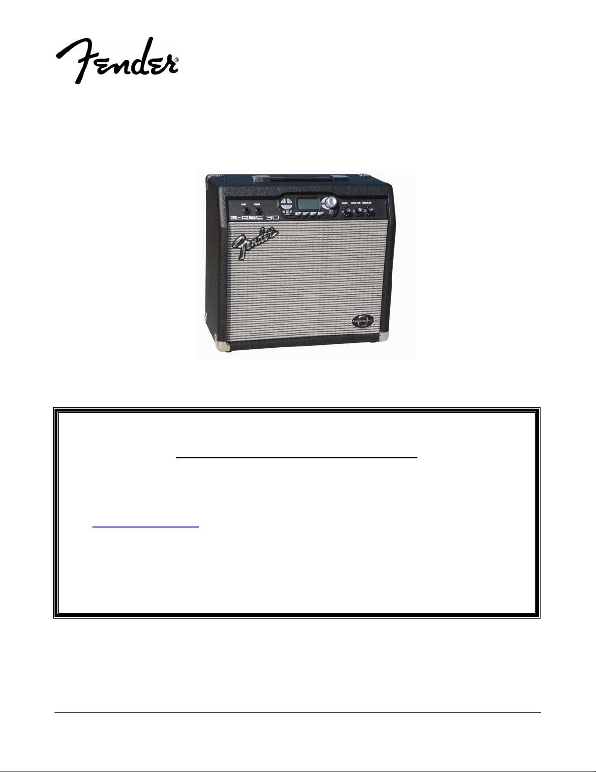
G-DEC®30
(This is the model name for warranty claims)
5
CIRCUIT DESCRIPTION
This section provides concise information about new
or unusual circuitry designs incorporated into this
amplifier model. The purpose is to aid the service
technician by providing insight into the design areas
most likely to become obstacles in troubleshooting.
Information is focused for its effective use while
maintaining the security of Fender® proprietary in-
formation wherever possible.
Note: Troubleshooting to component level on
the Main and Keypad PCBs is best accomplished
in Self-Test Mode (pass thru screen). Refer to
Self-Test Procedure found after DSP PCB. All
test points found on the service diagram are lo-
cated on the Main PCB top for easy access.
MAIN PCB - ANALOG INPUTS/OUTPUTS
Op-amps U1A-B provide high impedance inputs to
the front and rear instrument inputs with 12db of in-
put gain. Op-amps U3A-B comprise differential
amps (unity gain) for increased noise immunity. Op-
amps U4A-B provide differential inputs with 12dB of
gain to the Aux In L&R signals. Buffer amplifiers
U50A-B, U51A-B, U12A-B, and U53A-B provide dif-
ferential inputs to the ADCs U11 and U21. These
stages attenuate 15dB to compensate the for the full
scale input voltage of the ADCs. These inputs are
biased to +2.51VDC reference voltage from the VQ
pins on U11 and U21.
Op-amps U52A-B act as a differential reconstruction
filter (anti-aliasing) for the main (instrument, aux in,
MIDI) stereo output signals received from DAC U6,
and stereo Line Out signals from DAC U30.
Op-amps U24A-B and followers U14A-B provide
12dB of gain and sufficient current capability to drive
the stereo Phones jack.
MAIN PCB - POWER AMPLIFIER
Input signal is applied to the power amp at C120.
The power amplifier U10 (LM3886) is provided nega-
tive current feedback from sense resistor R119
through C92 and R112. DC feedback is provided by
network R102, R108, and C92. Current feedback
affects the power amplifier output resistance so it re-
acts with the speaker load similar to a tube amplifier.
The main internal speaker (8ohms minimum load) is
connected at P3-4. The internal speaker is discon-
nected if a connection is made to the External
Speaker Out jack J8.
MAIN PCB - POWER IC BIAS/MUTE PIN
Power IC U10 (LM3886) has a bias/mute pin which
requires >1mA of current for the amplifier to come
out of mute. When AC power is first applied, the
base of Q11 is held at -31VDC keeping Q11 off and
preventing current flow from bias pin U10.8. The
power amplifier remains muted until C118 charges to
a voltage above zener D11 (10V) and Q11 Vbe (ap-
proximately -21VDC) and Q11 turns on allowing
current to flow.
If nothing is plugged into the Phones jack, R48 is
held at ground turning on PNP transistor Q8. With
Q8 on, the collector of Q8 is at +5VDC driving the
base of Q6 to above -5.5VDC. Zener D10 clamps
the emitter of Q6 to -6VDC. With the base of Q6
above -6VDC, Q6 turns on allowing current to flow
from bias pin U10.8 bringing the amplifier out of
mute. If headphones (or other ¼” plug) are con-
nected to the Phones jack, R48 is lifted from ground
turning off Q8. This forces the base of Q6 to below
-6VDC shuting it off and preventing current from
flowing from bias pin U10.8 muting the amplifier.
The current through Q11 is now shunted from D10.