Furuno 1715 User manual

MARINE RADAR
MODEL 1715

Your Local Agent/DealerYour Local Agent/Dealer
9-52 Ashihara-cho,9-52 Ashihara-cho,
Nishinomi
y
a, Ja
p
anNishinomi
y
a, Ja
p
an
Tele
p
hone :Tele
p
hone : 0798-65-21110798-65-2111
fa
x
fa
x
0798-65-42000798-65-4200
::
F
IRST EDITION :
F
IRST EDITION : SEP.SEP. 20032003
Printed in JapanPrinted in Japan
A
ll ri
g
hts reserved.
A
ll ri
g
hts reserved.
PUB.No.PUB.No. SME-35140-ASME-35140-A
*00014876000**00014876000*
*00014876000**00014876000*
(( KAOKKAOK )) MODEL1715MODEL1715
* 0 0 0 1 4 8 7 6 0 0 0 ** 0 0 0 1 4 8 7 6 0 0 0 *
*SME35140A00**SME35140A00*
* S M E 3 5 1 4 0 A 0 0 ** S M E 3 5 1 4 0 A 0 0 *

Chapter 1 Circuit Description
1.1 General...........................................................................................................................1
1.2 Display unit....................................................................................................................2
1.3 Scanner unit...................................................................................................................6
Chapter 2 Location of Parts
2.1 Display unit....................................................................................................................10
2.2 Scanner unit...................................................................................................................11
Chapter 3 Adjustment
3.1 Display unit....................................................................................................................13
3.2 Scanner unit...................................................................................................................13
Chapter 4 Maintenance
4.1 Removing display unit cover.........................................................................................14
4.2 Replacement of Major Parts in Display unit..................................................................15
(1) DU board............................................................................................................15
(2) LCD unit ............................................................................................................15
(3) PNL board..........................................................................................................15
4.3 Replacement of Major Parts in Scanner unit.................................................................16
4.4 Synchronous Belt and Motor.........................................................................................17
4.5 Magnetron......................................................................................................................18
4.6 MIC................................................................................................................................18
4.7 Program updating ..........................................................................................................19
Chapter 5 Troubleshooting
5.1 Error Messages..............................................................................................................22
5.2 Troubleshooting Matrix table.....................................................................................................22
Content
s

Contents
5.3 Self Test..........................................................................................................................................24
5.3.1 Display unit.....................................................................................................24
5.3.2 Scanner unit....................................................................................................27
5.4 Test points on each board ..............................................................................................28
1) DU board (03P9320)...........................................................................................28
2) MD board (03P9270) ..........................................................................................28
3) INT board (03P9322) ..........................................................................................29
4) STC waveform ....................................................................................................29
Exploded View................................................................................. D-1
Electrical Parts List......................................................................... E-1
Schematic Diagrams....................................................................... S-1

Chapter 1 Circuit Description
1
1.1 General
The CPUs in the display and scanner units communicate each other via RS-422 interface. The
control data, such as Gain, STC and tuning data, is sent from the display unit to the scanner unit
in serial.
DU
LCD
BP HD
H.C
H.C
INT
I/F
MD
IF
IF
Fig.1-1 Simplified Block Diagram
The trigger pulse is generated on DU board in the display unit and sent to the modulator on MD
board in the scanner unit. The modulated signal triggers the magnetron and high frequency
pulses are transmitted from the radiator. The target echo received by the radiator is
frequency-converted by the MIC. 60 MHz IF signal is amplified in the scanner unit and then sent
to the display unit. DU board in the display unit processes video signal to show target echoes on
the LCD display.
Bearing pulse (BP) and heading signal (HD) are also delivered to the display unit from the
scanner unit.
Radiator
Scanner unit
Transceiver
LCD
Trigger
Display unit
MD
Board Video signal
IF
Board
INT
Board Communication (H.C)
Ship’s mains
PNL Board
BP/HD DU Board
Ship’s mains (H.C)
Signal processor
& power supply

1.2 Display unit
2
1.2 Display unit
TX trigger pulse is generated by gate array, U79 and sent to the scanner unit. The video signal
from the scanner unit is A/D converted and sampled by gate array, U78. Echoes in each sweep
are stored on the V-RAM via gate array, U79. Upon receiving the heading pulse, the stored data
are output to the LCD in four gradations, according to echo strength.
Fig.1-2 Block Diagram of Display Unit
LCD
HD/BP
DU Board
(03P9320)
TX trigger
Video signal
Scanner unit
Navaid
PNL Board
03P9330
Ship’s mains Power Supply

1.2 Display unit
3
The display unit consists of PNL board (03P9356), DU board (03P9320) and LCD unit
(EW50300FDWR). Each board functions as below.
PNL Board (03P9356)
This board functions as a man-machine interface, equipped with keys, LEDs for
panel-illumination, and a buzzer.
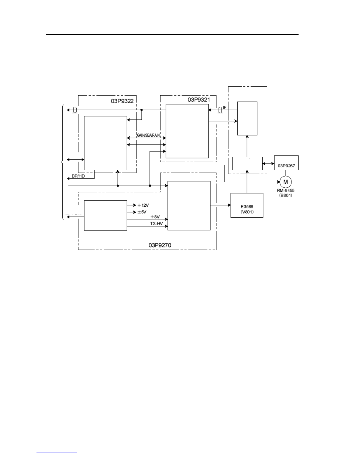
DU Board (03P9320)
According to the range setting, gate array U79 generates TX trigger pulses in specified pulse
repetition rate. Reference oscillator output is divided by the data from the CPU to decide the
PRR.
The pulse repetition rates differs slightly from set to set to prevent the radar interference.
The video signal from the scanner unit inputs to the video circuit on the DU board.
The video circuit includes FTC circuit that rejects the reflecting signals from the rain and snow.
CPU switches on or off the FTC according to control panel setting.
The video signal is converted by the A/D converter into seven-level digital signal, and input to
the radar signal processing circuit in the gate array U78. The digital video signal is sampled in
U78 with the sampling clock corresponding to the range setting. Further, when the interference
rejecter is turned on, each video signal is correlated with the corresponding transmission to
eliminate or reduce the radar interference signals. The processed video signal by U78 is written
into VRAMs via U79 for indication.
The bearing signal and heading signal are input to serial-to-parallel converter and then applied to
G/A U79 individually. Heading error obtained at heading alignment in installation menu is stored
in EEPROM U28, and used by CPU to calculate the correct antenna direction. TX time delay
data is also stored in EEPROM U28.
Unlike R/θcoordinate sweep, LCD display employs X-Y coordinate method similar to so called
TV- sweep method. U79 converts the R/θvideo signal to X-Y coordinates using formulas, RSIN
θand RCOS θ. The coordinate-converted video signal is written and maintained onto VRAM for
trail indication.
The data writing/reading onto/from the VRAM is carried out by U79 in time sharing. U79
retrieves data from VRAM to display it on the LCD display.
Scanner unit control data is converted to serial data by RS-422 interface, U27 and sent to the
scanner unit through a balanced RS-422 line. The control data includes transmission on/off, TX
pulsewidth selection, Gain and STC signals.
The data from the navigational aid is received through photo-couplers U10 and U11.

1.2 Display unit
4
Fig.1-3 Block Diagram of DU Board (03P9320)

1.2 Display unit
5
The unit operates on universal voltage ranging from 10.8 V to 31.2 V DC. This range covers the
voltage requirement for 12 V/24 V ship’s mains 10 % lower and 30 % higher. The ship’s mains is
supplied through a noise filter to the pulsewidth-controlled DC-DC converter which generates
the stable voltages; +5 V, +12 V, +8 V and –24 V. The ship’s mains is also supplied to the
scanner unit, bypassing the power supply circuit in the display unit. +5 V is mainly used for the
digital circuits, +12 V for the video circuits, +8 V for the backlight, and –24 V for the LCD
display. The DC-AC inverter consisting of Q33, Q34 and T1 generates 210 V AC for the
backlighting of the LCD display.
If the power supply is connected to the radar in reverse polarity, the reverse-polarity protector
activates so that the fuse is blown off to prevent the damage to the unit.
The power supply circuit contains low- and high-input voltage protector.

1.3 Scanner unit
6
1.3 Scanner unit
In the scanner unit, the TX trigger from the display unit is modulated to use it for triggering the
magnetron. The received echo is fed to the MIC and down-converted to 60 MHz IF signal.
Auto-gain and auto-STC circuits are not in the scanner unit, but in the display unit.
Fig.1-4 Block Diagram of Scanner Unit
Display
unit
Trigger
Interface
Auto Gain
Auto STC
Auto Tune
Communication
Motor Drive
INT Board
Magnetron
Ship’s
mains
Tune
Power Supply
MD Board
Modulator
COM
Video
IF AMP Tune
Antenna
Circulator
IF Board
MIC
RU-9458B
(U801)

1.3 Scanner unit
7
INT board (03P9322)
INT board mainly consists of CPU U4 that includes the RAM, ROM and analog ports, RS-422
interface U5, a motor drive circuit and a gain control signal generator.
CPU U4 receives control panel settings on the display unit through the RS422 interface U5. The
D/A converter U2 converts Gain, A/C RAIN, and tuning control signals from digital to analog.
A/C SEA and A/C RAIN circuit consisting of Q1, Q2 and Q3 outputs GAIN CONT signal to IF
board.
The CPU U4 controls the stepping motor drive circuit, Q4 to Q7 to keep the antenna rotation
speed constant.
The heading signal (HD) from the lead switch is mixed with the bearing pulse (BP) by Q9 to
Q11 and sent to the display unit.
The ship’s main is supplied to the power supply circuit on the MD board via INT board.
MD board generates +5 V, +12 V and -6 V for the use on INT board.
Fig.1-5 Block Diagram of INT Board (03P9322)
Display
unit
Step
motor
Waveform
generator
Interface
Mixer Serial
Serial
Conv.
Reset
Ref. Osc.
Video signal
Filter
Ship’s mains
Buffer
Trigger
Bandwidth switch
Buffer
Q4, Q5
Q6, Q7
Pulsewidth signal
MD
Board
Lead
Switch
IF
Board

1.3 Scanner unit
8
IF Amplifier board (03P9321)
The 60 MHz IF amplifier consists of Q1, Q2, U1 and U2, and provides the bandwidth of 7 MHz.
The tuning level detector, U3 to U8, detects the main bangs to indicate the tuning level.
Fig.1-6 Block Diagram of IF AMP Board (03P9321)
MIC (RU-9458B)
The circulator in the module switches between the transmitting and receiving microwave circuits
so that the transmitting radio energy is efficiently transmitted to the antenna without leaking to
the receiver side and the receiving radar signal from the antenna is sent with efficiency to the
receiver without leaking to the transmitter side.
The receiver circuit consists of a diode limiter, an RF amplifier, a balanced mixer and an FET
oscillator. The diode limiter protects the amplifier and balanced mixer from the excessive input
power. The mixer converts the input microwave signal to the 60 MHz IF signal. The oscillator is
voltage-controlled and outputs the signal to the mixer.
MD board (03P9270)
The MD board consists of a power supply circuit and a modulator.
There are two DC-DC converters in the power supply circuit: one generates –6 V, +5 V, and +12
V and the other magnetron heater voltage and TX HV. In the DC-DC converter, drivers Q803
and Q832 are driven by PWM controllers, U801 and U805 respectively.
The magnetron current, –6 V, +5 V, +12 V, +8 V (magnetron heater voltage), and TXHV can be
measured at the test point TP804.
The modulator in TX circuit receives the transmitting pulsewidth selection signals, PL-A and
PL-B, from INT board, and the trigger signal from the display unit. One-shot multivibrator U851
generates the transmitting trigger pulse of which the pulsewidth depends on range setting.
VR851 and VR852 adjust the output power of the magnetron. The pulse is boosted up by T851
and applied to the magnetron.
Q1
First
IF AMP
Video
signal
output
Third IFAMP
Video detector
U1
60 MHz IF
LC filter U1
Second
IF AMP
GAIN CONT signal
(From INT Board)
TUNE IND OUT
TUNE GATE IN Tuning level
detector
U3 to U8
60 MHz IF
LC filter
Video
amplifier
U2
9 V
VR2

1.3 Scanner unit
9
Fig.1-7 Block Diagram of MD board (03P9270)
Trans Reset

Chapter 2 Location of Parts
10
2.1 Display unit
Fig.2-1 DU board (03P9320)
TP6 (VIDEO) J1351 DJ1 J1352
TP12
(BUSCLK)
TP15 (RST)
TP17 (INV)
TP5
TP3 (+9V)
TP1 (Q6D)
VR1
TP16 (PWR OFF)
TP2 (+5V)
TP4 (GND)
J6
(EXT BUZZ)
J7 (RS 232C)
TP14 (HD)
TP11 (TRIG)
TP13 (BP)
TP8 (PWS)
J3
TP10 (PWL)
TP7
(
VIDEO OUT
)
TP9 (PWM)

2.2 Scanner unit
11
2.2 Scanner unit
Fig.2-2 INT board (03P9322)
Fig.2-3 IF board (03P9321)
J803TP2TP1TP4
TP5
J802
J805
TP3
J801 J804
J2J3
VR2
J1

2.2 Scanner unit
12
Fig.2-4 MD board (03P9270)
TP803 TP806 TP805 TP812
TP801 TP807 TP808
TP802 (COLD) VR801 TP811
TP814
VR852
VR851

Chapter 3 Adjustment
13
DANGER- High voltage
The display unit contains 1 kVAC for LCD backlighting and
the scanner unit 300 VDC for TX.
3.1 Display unit
+5 V is adjusted by VR1 on DU board. See Fig.3-1 for the location of parts.
Table 3-1 Test points of Display unit
Item Setting Test point Ratings Adjuster
+5 V TX (8 NM) TP4 (+), TP5 (-) 4.95 to 5.05 Vdc VR1
+12 V ST-BY J1#7 (+), J1#5 (-) 11.2 to 12.4 Vdc
-22 V ST-BY J1#10 (+), J1#5 (-) -22.9 to -20.7 Vdc
-6 V ST-BY J1#9 (+), J1#5 (-) -6.0 to -5.0 Vdc
Fig.3-1 Location of J1 and J8 on DU board
3.2 Scanner unit
Adjusters on MD board in the scanner unit are adjusted as below.
Table 3-2 Test points of Scanner unit
Item Setting Test point Rating Adjuster
+12 V ST-BY TP804#3 (+)
TP804#4 (-) 11.9 to 12.1 Vdc VR801
+8 V
heater volt. ST-BY TP804#6 (+)
TP804#4 (-) 7.8 to 8.2 Vdc
TX-HV
(divided) ST-BY TP804#7 (+)
TP804#4 (-) 8.5 to 9.35 V
Long 3.05 to 3.15 V VR851
Magnetron
current TX TP804#5 (+)
TP804#4 (-) Short 3.35 to 3.45 V VR852
TP2
DU Board
(03P9320)
J8 J1

Chapter 4 Maintenance
14
This unit is designed for board level maintenance. Thus, component replacement is not
recommended.
4.1 Removing display unit cover
To remove the display unit cover:
1. Remove three connector nuts on the display unit cover.
2. Remove six screws fixing the display unit cover to the front panel.
3. Find a slot at both sides of the unit. (Fig.4-2) The display unit cover has locking mechanism.
4. Insert a coin into the slot on the left side of the display unit. Giving a little bit of force,
separate the cover. Do the same at the right side.
5. When replacing the cover, confirm that the connector packing is seated in position.
Fig. 4-1 Display Unit, Rear View
Fig. 4-2
(a) Hole for locking tab on the
front panel (b) Locking protrusion on the cover

4.2 Replacement of Major Parts in Display unit
15
4.2 Replacement of Major Parts in Display unit
(1) DU board
To remove DU board;
1. Disconnect the FPC and the LCD lamp connector.
2. To remove DU board, loosen four screws ringed in Fig.4-3.
3. Pull DU board up straighytly.
(2) LCD unit
To remove LCD unit;
4. Loosen three screws ringed in Fig.4-4.
5. Remove the LCD unit together with the mounting plate.
6. Separate the LCD unit from the mounting plate by loosening a screw at each corner.
Fig.4-3 Fig.4-4
(3) PNL board
To remove LCD unit, loosen screws which
secure the P.C. board to the panel.
Fig.4-5
LCD lamp connector
HIGH VOLTAGE!
DU board
Non-lock t
yp
e FPC connector
PNL board

4.3 Replacement of Major Parts in Scanner unit
16
4.3 Replacement of Major Parts in Scanner unit
Fig.4-6 shows screws which fix boards to the chassis.
Fig.4-6 Boards in Scanner unit
MD board (03P9270A)
Heat sink sheet
03-146-3309
M3 X 8 (6 pcs.)
M4 X 20 Heat sink plate
03-146-3305
M3 X 8 (4Pcs.)
IF board (03P9321)
M3 X 8 (4 pcs.)
INT board
(03P9322)
Other manuals for 1715
4
Table of contents
Other Furuno Marine Radar manuals

Furuno
Furuno FR-2135S User manual

Furuno
Furuno 1823C-BB User manual

Furuno
Furuno FR-8051 User manual

Furuno
Furuno FAR-1513 User manual

Furuno
Furuno FR-8051 User manual

Furuno
Furuno FAR-2218 Manual

Furuno
Furuno FR-810DS User manual

Furuno
Furuno FCR-902 User manual

Furuno
Furuno FR-7041R-MARK-2 User manual

Furuno
Furuno FR-602D User manual

Furuno
Furuno FE-700 User manual

Furuno
Furuno 1823C-BB User manual

Furuno
Furuno 1715 Manual

Furuno
Furuno FR-7061 User manual

Furuno
Furuno Navnet VX2 User manual

Furuno
Furuno FR1500 Mk3 User manual

Furuno
Furuno FAR-2137S-BB User manual

Furuno
Furuno BBDS1 User manual

Furuno
Furuno FAR-2117 User manual

Furuno
Furuno 1931 User manual