G.B.T GA-BX2000 User manual

BX2000
1
TABLE OF CONTENTS
1. INTRODUCTION
1.1. PREFACE.......................................................................................................1-1
1.2. KEY FEATHERS............................................................................................1-1
1.3. PERFORMANCE LIST...................................................................................1-2
1.4. BLOCK DIAGRAM..........................................................................................1-3
1.5. INTRODUCE THE PENTIUMII / III PROCESSORS.................................1-4
1.6. WHAT IS AGP?..............................................................................................1-5
2. SPECIFICATION
2.1. HARDWARE ..................................................................................................2-1
2.2. SOFTWARE...................................................................................................2-2
2.3. ENVIRONMENT.............................................................................................2-2
3. HARDWARE INSTALLATION
3.1. UNPACKING..................................................................................................3-1
3.2. MAINBOARD LAYOUT..................................................................................3-2
3.3. QUICK REFERENCE FOR JUMPERS & CONNECTORS...........................3-2
3.4. DRAM INSTALLATION..................................................................................3-6
3.5. CPU SPEED SETUP......................................................................................3-6
3.6. CMOS RTC & ISA CFG CMOS SRAM..........................................................3-7
3.7. SPEAKER CONNECTOR INSTALLATION...................................................3-8
3.8. HARDWARE RESET SWITCH CONNECTOR INSTALLATION.................3-8
3.9. POWER LED CONNECTOR INSTALLATION..............................................3-8
3.10. IDE & ATAPI DEVICE INSTALLATION.......................................................3-8

Table of Contents
2
3.11. PERIPHERAL DEVICE INSTALLATION.....................................................3-8
3.12. KEYBOARD & PS/2 MOUSE INSTALLATION............................................3-8
4. BIOS CONFIGURATION
4.1. ENTERING SETUP........................................................................................4-1
4.2. CONTROL KEYS ...........................................................................................4-1
4.3. GETTING HELP.............................................................................................4-2
4.3.1. Main Menu .....................................................................................4-2
4.3.2. Status Page Setup Menu / Option Page Setup Menu..........................4-2
4.4. THE MAIN MENU...........................................................................................4-2
4.5. STANDARD CMOS SETUP MENU...............................................................4-4
4.6. BIOS FEATURES SETUP .............................................................................4-8
4.7. CHIPSET FEATURES SETUP......................................................................4-13
4.8. POWER MANAGEMENT SETUP.................................................................4-17
4.9. PNP/PCI CONFIGURATION........................................................................4-21
4.10. LOAD BIOS DEFAULTS..............................................................................4-23
4.11. LOAD PERFORMANCE DEFAULTS ..........................................................4-24
4.12. INTEGRATED PERIPHERALS....................................................................4-25
4.13. SPUERVISOR PASSOWORD/USER PASSWORD ..................................4-30
4.14. IDE HDD AUTO DETECTION.....................................................................4-31
4.15. SAVE & EXIT SETUP ..................................................................................4-32
4.16. EXIT WITHOUT SAVING ............................................................................4-33

BX2000
1-1
1. INTRODUCTION
1.1. PREFACE
Welcome to use the BX2000 motherboard. It is a PentiumII / III / Celeron
Processor based PC /AT compatible system with AGP / PCI / ISA Bus, and
has been designed to be the fastest PC / AT system. There are some new
features allow you to operate the system with just the performance you want.
This manual also explains how to install the motherboard for operation, and
how to set up your CMOS CONFIGURATION with BIOS SETUP program.
1.2. KEY FEATURES
qIntel PentiumII / III / Celeron Processor based PC / AT compatible
main board.
qSlot 1 supports PentiumII / III / Celeron processor running at 233-650
MHz.
qIntel 440BX chipset, Supports AGP / SDRAM / Ultra DMA/33 IDE /
Keyboard and PS/2 Mouse Power On / ACPI features.
qSupports 4xDIMMs using 3.3V SDRAM DIMM module.
qSupports Intel LDCMNetwork Manageability.
qSupports 8 MB –1GB SDRAM memory on board.
qSupports ECC or Non-ECC type DRAM module.
q1xAGP slot, 5xPCI Bus slots, 2xISA Bus slots.
qSupports 2 channels Ultra DMA/33 IDE ports for 4 IDE Devices.
qSupports 2xCOM (16550), 1xLPT (EPP / ECP), 1x Floppy port.
qSupports 2xUSB ports, 1xPS/2 Mouse & 1xPS/2 Keyboard.
qLicensed AWARD BIOS, 2M bits FLASH RAM.
qSupport Dual BIOS.
qSupport Suspend To RAM Function.
qSupport CPU Over Voltage Protect.

Introduction
1-2
q30.5 cm x 19 cm ATX SIZE form factor, 4 layers PCB.

BX2000
1-3
1.3. PERFORMANCE LIST
The following performance data list is the testing results of some popular
benchmark testing programs.
These data are just referred by users, and there is no responsibility for
different testing data values gotten by users. (Different Hardware & Software
configuration will result in different benchmark testing results.)
•CPU PentiumII / III processor
•DRAM (32 x 2) MB SDRAM (MICRON MT 48LC2M8A1 -8)
•CACHE SIZE 512 KB included in CPU
•DISPLAY GA-630 AGP Display Card (4MB SGRAM)
•STORAGE Onboard IDE (Seagate ST34520A)
•O.S. Windows NT™4.0 (Service Pack 4)
•DRIVER Display Driver at 1024 x 768 x 16bit colors x 75Hz.
TRIONES Bus Master IDE Driver 3.60
Intel PentiumII / III
Processor 350MHz(100x3.5) 500MHz(100x5)
Winbench99
CPU mark32 906 1260
FPU Winmark 1800 2550
Business Disk 4260 4440
Hi-End Disk 10400 10600
Business Graphics 169 227
Hi-End Graphics 292 403
Winstone99Business 27.4 33
Hi-End 24.9 30.8
Introduction
1-4
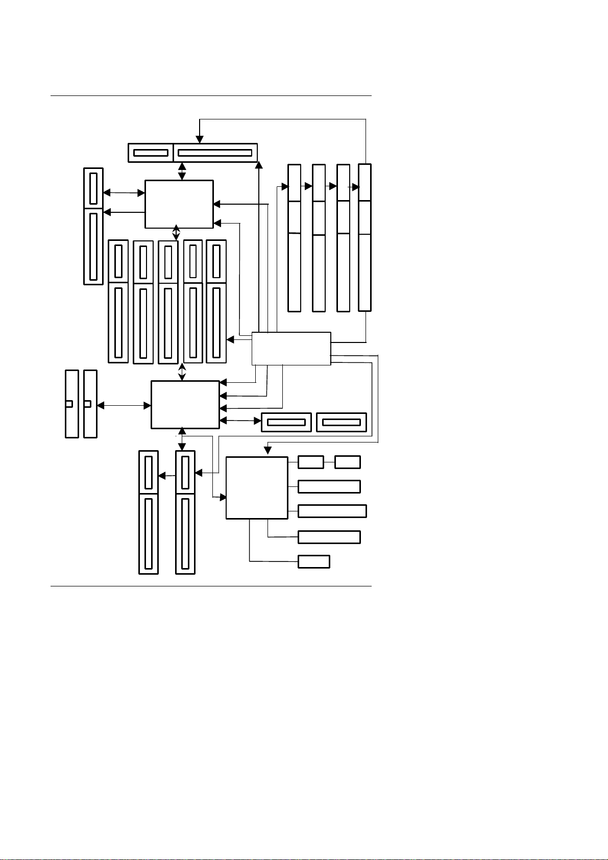
1.4. BLOCK DIAGRAM
24MHz
3.3V SDRAM
DIMM Sockets
14.318MHz
33 MHz
33MHz
Ultra DMA/33
IDE Ports
IDE Bus
PCI Bus
ISA Bus
AGP Bus
LPT Port
Keyboard
Floppy Port
COM Ports
PS/2 Mouse
USB Bus
14.318MHz
48MHz
14.318MHz
I/O
CHIPSET
ITE 8671
AGP
Host Bus
INTEL
82443BX
CHIPSET
PIIX4
82371EB
CHIPSET
ICS 9248-55 /
9279-01
SLOT 1
66MHz
66 /
100 MHz
66 /
100 MHz
33 MHz
66 /
100 MHz

BX2000
1-5
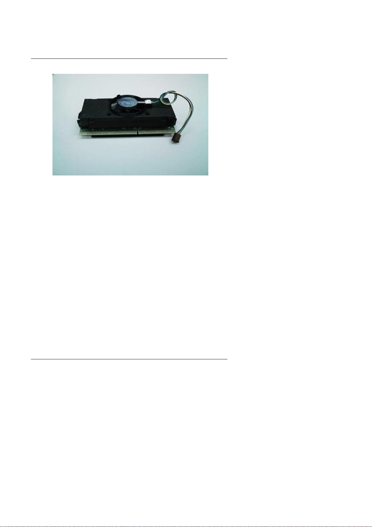
1.5. INTRODUCE THE Pentium
II / III Processors
Figure 1: Universal Retention Mechanism & attach Mount
Figure 2:OEM PentiumII Processor
Introduction
1-6
Figure 3: OEM PentiumIII Processor
1.6 What is AGP
?
The Accelerated Graphics Port (AGP) is a new port on the Host-To-PCI
bridge device that supports an AGP port. The main purpose of the AGP port
is to provide fast access to system memory.
The AGP port can be used either as fast PCI port (32-bits at 66MHz vs.32-
Bits at 33MHz) or as an AGP port which supports 2x data-rate, a read queue,
and side band addressing. When the 2x-data rate is used the port can
transmit data at 533MB/sec (66.6*2*4). The read-queue can be used to
pipeline reads –removing the effects of the reads-latency. Side band
addressing can be used to transmit the data address on a separate line in
order to speed up the transaction.

Specification
2-1
2. SPECIFICATION
2.1. HARDWARE
•CPU −PentiumII/III/Celeron processor 233 –650 MHz.
−242 pins 66 / 100MHz slot1 on board.
•PROTECTION −Supports CPU Over Voltage Protect.
−Speaker Alarm when detect "CPU FAN Failure" or
“CPU Overheat”.
−Automatically slow down CPU speed when "CPU
Overheat".
−Intel LDCMsupported.
−H/W monitor power status (±5V, ±12V,
VGTL,5VSB, CPU voltage & CMOS battery
voltage).(Optional)
•SPEED −66/100 MHz system speed.
−66 MHz AGP bus speed. (2X mode 133MHz)
−33 MHz PCI-Bus speed.
−8 MHz AT bus speed.
•DRAM MEMORY −4 banks 168 pins DIMM module sockets on board.
−Use 8 / 16 / 32 / 64 / 128 / 256 MB DIMM module
DRAM.
−8 ~ 1GB SDRAM.
−Supports 3.3V SDRAM.
−Supports ECC or Non-ECC type DRAM.
−Supports Suspend To RAM Function.
•CACHE MEMORY −32 KB L1 cache memory included in CPU.
−128KB / 512 KB L2 cache memory included in
CPU.
−Supports DIB speed mode for L2 Cache.
•I/O BUS SLOTS −5 33MHz Master / Slave PCI-BUS.
−2 8MHz 16 bits ISA BUS.
−1 66MHz / 133MHz AGP bus.
•IDE PORTS −2 Ultra DMA/33 Bus Master IDE channels onboard.
(Using IRQ14,15)

BX2000
2-2
−Support Mode 3,4 IDE & ATAPI CD –ROM.
•I/O PORTS −Supports 2 16550 COM ports.
−Supports 1 EPP/ECP LPT port.
−Supports 1 Floppy port.
−Supports 2 USB ports.
−Supports PS/2 Mouse & PS/2 Keyboard.
•GREEN FUNCTION −Suspend mode support.
−Green switch & ACPI LED support.
−IDE & Display power down support.
−Monitor all IRQ / DMA / Display / I/O events.
•BIOS −2M bits FLASH RAM.
−Support Dual BIOS.
−Supports Plug & Play, DMI , ACPI Function.
•DIMENSION −ATX Form Factor, 4 layers PCB.
2.2. SOFTWARE
•DRIVER −INTEL Bus Master IDE Driver.
−Suspend to HD utility.
−INTEL LDCM®.
•BIOS −Licensed AWARD BIOS.
−AT CMOS Setup, BIOS / Chipset Setup, Green
Setup, Hard Disk Utility included.
•O.S. −Operation with MS-DOS, Windows95,
Windows98, WINDOWS NT™, OS/2, NOVELL
and SCO UNIX.
2.3. ENVIRONMENT
•Ambient Temp. −0°C to +50°C (Operating).
•Relative Hum. −0 to +85% (Operating).
•Altitude −0 to 10,000 feet (Operating).
•Vibration −0 to 1,000 Hz.
•Electricity −4.9 V to 5.2 V. (Max. 20A current at 5V.)

Hardware Installation
3-1
3. HARDWARE INSTALLATION
3.1. UNPACKING
The main board package should contain the following:
•The BX2000 main board.
•The Universal Retention Mechanism & Attach Mount
•USER’S MANUAL for main board.
•Cable set for IDE, Floppy devices.
•Diskette or CD for main board Utility.
The main board contains sensitive electric components, which can be easily
damaged by static electricity, so the main board should be left in its original
packing until it is installed.
Unpacking and installation should be done on a grounded anti-static mat.
The operator should be wearing an anti static wristband, grounded at the
same point as the anti-static mat.
Inspect the main board carton for obvious damage. Shipping and handling
may cause damage to your board. Be sure there are no shipping and
handling damages on the board before proceeding.
After opening the main board carton, extract the system board and place it
only on a grounded anti-static surface component side up. Again inspect the
board for damage. Press down on all of the socket IC's to make sure that
they are properly seated. Do this only on with the board placed on a firm flat
surface.
M
DO NOT APPLY POWER TO THE BOARD IF IT HAS BEEN DAMAGED.
BX2000
3-2
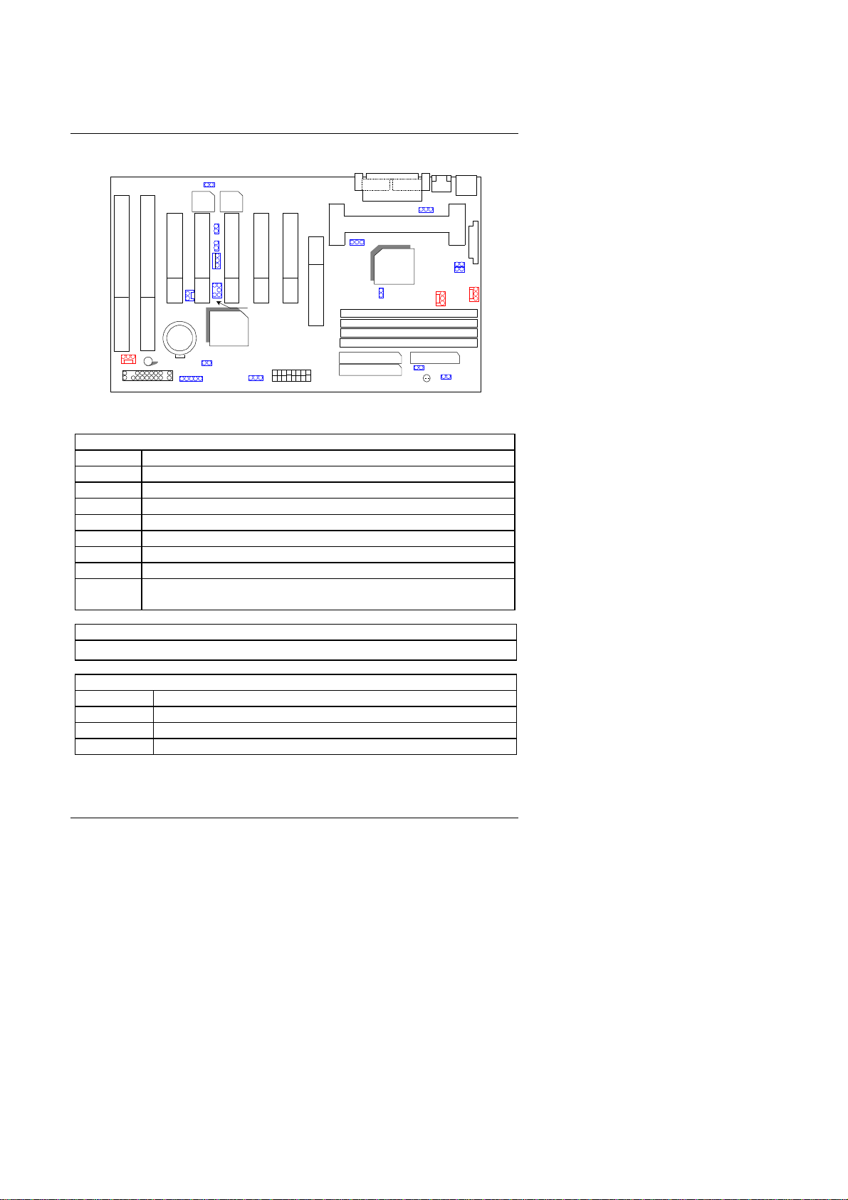
3.2. MAINBOARD LAYOUT
CPU
Intel
440BX
PIIX4
BX2000
Main
BIOS
Backup
BIOS
SW IDE 1
IDE 2 Floppy
DRAM
LED
JP16 JP13
BANK 0
BANK 1
BANK 2
BANK 3
JP14
IR
PANEL(SYSTEM) FAN
BZ 1
BAT
J15
SB-LINK
JP18
JP12
JP17
JP11
POWER
FAN
CPU
FAN
ATX
POWER
PS/2USB
COM A COM B
LPT JP1
PCI 2
PCI 3
PCI 4
PCI 5
ISA 1
ISA 2
JP9
JP19
JP20
JP21
×Figure 3.1Ø
3.3. QUICK REFERENCE FOR JUMPERS & CONNECTORS
tI/O Ports Connector
USB USB port.
PS/2 For PS/2 Keyboard / Mouse port.
IDE 1 For Primary IDE port.
IDE 2 For Secondary IDE port.
Floppy For Floppy port
COM B For Serial port2 (COM B).[Support External Modem Ring On]
COM A For Serial port1 (COM A).[Support External Modem Ring On]
LPT For LPT port.
ATX
POWER For ATX Power Connector.
tSlot 1
For PentiumII / III / Celeron Processor installed
tCPU FAN : CPU Cooling FAN Power Connector
Pin No. Function
1GND.
2+12V
3SENSE
Hardware Installation
3-3
tPOWER FAN : POWER FAN Power Connector
Pin No. Function
1GND.
2+12V
3SENSE
tPANEL(SYSTEM) FAN: PANEL(SYSTEM) FAN Power Connector
Pin No. Function
1GND.
2+12V
3SENSE
tJ15 : System After Ac Back
Open Soft Off (Default)
Short Full On
tJP1 : Keyboard Power On Selection
Pin No. Function
1-2 short Enabled Keyboard power on.
2-3 short Disabled Keyboard power on.(Default)
tJP11 : System Acceleration
1-2 short For 100MHz Turbo and other frequencies
2-3 short For 100MHz Normal (Default)
tJP7 : Wake on LAN Connector
Pin No. Function
1+5VSB
2GND
3CTRL-Signal
tJP12 : CASE OPEN
Pin No. Function
1Signal
2GND

BX2000
3-4
tSB-LINK : For PCI Sound Card Connector
Pin No. Function
1Signal
2GND
3NC
4Signal
5GND
6Signal
tIR: INFRARED Connector (OPTIONAL)
Pin No. Function
1IR DATA OUTPUT
2GND
3IR DATA INPUT
4NC
5POWER(+)
tJP14 : CLEAR CMOS
Pin No. Function
1-2 short Clear CMOS
2-3 short Normal (Default)
tJP18/ JP19 : Single/Dual BIOS (OPTIONAL)
Pin No. Function
Open Dual BIOS (Default)
Short Single BIOS
tJP13 / JP17 :Close STR Enable
Pin No. Function
1Signal
2GND
tRING POW ON
Pin No. Function
1Signal
2GND
tJP20 & JP21 (For PCB:1.1 and after use)

Hardware Installation
3-5
Pin No. Function
Open Normal (Default)
Short Close for Voodoo III VGA Card.
JP9 : 2*11PIN Jumper
PW : Soft Power Connector
Open: Normal Operation
Short: Power On/Off
RE : Reset Switch
Open: Normal Operation
Short: For Hardware Reset System
P+P
−
P
−
: Power LED
PIN 1 : anode (+)
PIN 2 : cathode (−)
PIN 3 : cathode (−)
SPKR : External Speaker Connector
PIN 1 : VCC (+)
PIN 2 : VCC
PIN 3 : Data
PIN 4 : Data (−)
SPKR : Internal Speaker Connector (Default)
PIN 1 : VCC (+)
PIN 2-PIN3 : Short
PIN 4 : Data (−)
1
1+
−
JP9
PW P+P−P−H+
RE SPKR
GN
G−
1
1 1
1H−GN
G+
1+
−

BX2000
3-6
H+H
−
: IDE Hard Disk Active LED
PIN 1: LED anode (+)
PIN 2: LED cathode (−)
GN: Green Function Switch
Open : Normal operation
Short : Entering Green Mode
G
−
G+: Green LED
PIN 1 : LED anode (+)
PIN 2 : LED cathode (−)
3.4. DRAM INSTALLATION
The main board can be installed with 8 / 16 / 32 / 64 / 128 / 256 MB 168
pins DIMM module DRAM, and the DRAM speed must be 67~100 MHz for
SDRAM when system bus speed is set to 66MHz. When system bus speed
is set to 100MHz, 100MHz SDRAM is required. The DRAM memory system
on main board consists of bank 0, 1, 2 & bank 3.
Since 168 pins DIMM module is 64 bits width, therefore 1 piece of DIMM
module may match a 64 bits system. The total memory size is 8 MB ~1GB
SDRAM. The DRAM installation position refer to Figure 3.1, and notice the
Pin 1 of DIMM module must match with the Pin 1 of DIMM socket. Insert the
DRAM DIMM module into the DIMM socket at Vertical angle. If there is a
wrong direction of Pin 1, the DRAM DIMM module could not be inserted into
socket completely.
3.5. CPU SPEED SETUP
The system bus speed can be set to 66 / 100MHz form the DIP SWITCH
(SW). The user can change the DIP SWITCH selection to set up the CPU
speed for different processors.
1
1

Hardware Installation
3-7
ON: m
OFF: 5
PentiumII / III
CPU 1 2 3 4 5 6 7 8
233 / 66MHz
55mmm55m
266 / 66MHz
m m 5mm55m
300 / 66MHz
5m5mm55m
333 / 66MHz
m5 5 mm55m
366 / 66MHz
5 5 5 mm55m
400 / 66MHz
mmm5m55m
433 / 66MHz
5mm5m55m
350 / 100MHz
55m m 5 5 5 5
400 / 100MHz
m m 5m5 5 5 5
450 / 100MHz
5m5m5 5 5 5
500 / 100MHz
m5 5 m5 5 5 5
550 / 100MHz
5 5 5 m5 5 5 5
600 / 100MHz
mmm5 5 5 5 5
650 / 100MHz
5mm5 5 5 5 5
M
The CPU is a sensitive electric component and it can be easily
damaged by static electricity, so users must keep it away from
metal surface when the CPU is installed onto main board.
3.6. CMOS RTC & ISA CFG CMOS SRAM
There're RTC & CMOS SRAM on board; they have a power supply from
external battery to keep the DATA inviolate & effective. The RTC is a REAL-
TIME CLOCK device, which provides the DATE & TIME to system. The
CMOS SRAM is used for keeping the information of system configuration, so
the system can automatically boot OS every time. Since the lifetime of
internal battery is 5 years, the user can change a new Battery to replace old
one after it cannot work.
MDanger of explosion if battery is incorrectly replaced.

BX2000
3-8
MReplace only with the same or equivalent type recommended by the
manufacturer.
MDispose of used batteries according to the manufacturer’s instructions.
3.7. SPEAKER CONNECTOR INSTALLATION
There is a speaker in AT system for sound purpose. The 4 -Pins connector
SPKR is used to connect speaker. Anode connects +, Cathode connects −.
3.8. HARDWARE RESET SWITCH CONNECTOR INSTALLATION
The RESET switch on panel provides users with HARDWARE RESET
function. The system will do a cold start after the RESET switch is pushed
and released by user. The RESET switch is a 2 PIN connector and should be
installed to RST on main board.
3.9. POWER LED CONNECTOR INSTALLATION
System has Power LED lamp on the panel of case. The Power LED will light
on off or flash to indicate which step on the system. The connector should be
connected to PWR of main board in correct direction.
3.10. IDE & ATAPI DEVICE INSTALLATION
There are two-Enhanced PCI IDE ports (IDE1, IDE2) on board, which
following ATAPI standard SPEC. Any one IDE port can connected to two
ATAPI devices (IDE Hard Disk, CD-ROM & Tape Driver), so total four ATAPI
devices can exist in a system. The HD is the active LED port for ATAPI
devices.
3.11. PERIPHERAL DEVICE INSTALLATION
After the I/O device installation and jumpers setup, the main board can be
mounted into the case and fixed by screw. To complete the main board
installation, the peripheral device could be installed now. The basic system
needs a display interface card. If the PCI - Bus device is to be installed in the
system, any one of four PCI - Bus slots can be used.
3.12. KEYBOARD & PS/2 MOUSE INSTALLATION

Hardware Installation
3-9
The main board supports PS/2 Mouse. The BIOS will auto detect whether the
PS/2 Mouse is installed or not & assign IRQ12 for PS/2 Mouse port if it is
installed. After installing the peripheral device, the user should check
everything again, and prepare to power-on the system.

BIOS Configuration
4-1
4.BIOS CONFIGURATION
Award's BIOS ROM has a built-in Setup program that allows users to modify
the basic system configuration. This type of information is stored in battery-
backed CMOS SRAM so that it retains the Setup information when the power
is turned off.
4.1. ENTERING SETUP
Power ON the computer and press <Del> immediately will allow you to enter
Setup. If the message disappears before you respond and you still wish to
enter Setup, restart the system to try again by turning it OFF then ON or
pressing the "RESET" bottom on the system case. You may also restart by
simultaneously press <Ctrl>, <Alt>, and <Del> keys.
4.2. CONTROL KEYS
Up arrow Move to previous item
Down arrow Move to next item
Left arrow Move to the item in the left hand
Right arrow Move to the item in the right hand
Esc key Main Menu - Quit and not save changes into CMOS
Status Page Setup Menu and Option Page Setup Menu -
Exit current page and return to Main Menu
PgUp key Increase the numeric value or make changes
PgDn key Decrease the numeric value or make changes
F1 key General help, only for Status Page Setup Menu and
Option Page Setup Menu
F2 key Change color from total 16 colors
F3 key Reserved
F4 key Reserved
F5 key Restore the previous CMOS value from CMOS, only for
Option Page Setup Menu
F6 key Load the default CMOS value from BIOS default table,
only for Option Page Setup Menu
F7 key Load the default
F8 key Reserved
F9 key Reserved
F10 key Save all the CMOS changes, only for Main Menu
Table of contents
Other G.B.T Motherboard manuals


Popular Motherboard manuals by other brands


e-nova
e-nova X-Wall DX quick guide

PCchips
PCchips M935 Series user manual

Global American Inc.
Global American Inc. 2807632 user manual

ARTESYN EMBEDDED TECHNOLOGIES
ARTESYN EMBEDDED TECHNOLOGIES ATCA-7370 Installation and use

Global American Inc.
Global American Inc. 2807660 Series user manual

Sercomm
Sercomm TPM540 EVK user guide


