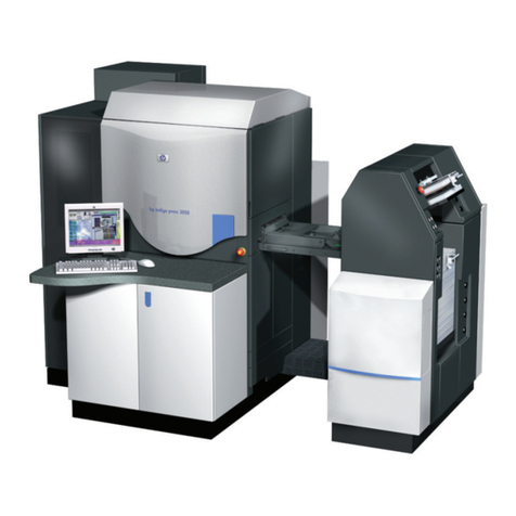
HP 654A Service manual

Fli;'
HEWLETT
.:e.
PACKARD
OPERATING
AND
SERVICE
MANUAL
MODEL
654A
TEST
OSCILLATOR
The
main
bod
y
of
this
manual
appli
es
to
Seria l Pre fix
0951
A
Any
changes
made
in
instruments
manufactured
after
this
printing
w i
ll
be
found
in
a
"Manual
Chan
g
es
"
supplem
e
nt
supplied
with
this
manual
. Be
su
re
to
ex
amine
this
s
upplement,
if
one
ex
ist
s
for
thi
s
manual,
fo
r
any
changes
which
apply
to
your
instrum
e
nt
and
record
these changes
in
the
manual.
Backdating
information
for
in
st
rum
e
n~s
ma
n
ufactured
before
thi
s
printing
will
be
found
in
Appendix
C
for
in s
trume
nt Serial
Numbers
0951
A02260
and b e
low
.
WARNING
I
To
help
minimize
the
possibility
of
electrical
fire
or
shock
hazards,
do
not
expose
this
instrument
to
rain
or
excess
moisture.
·hp- Part No. 00654-90003
Microfiche Part No. 00654-90053
© Copyright Hewlett-Packard
Company
1969
P .O. Box
30),
Loveland ,
Colorado
80537
U.S.A.
Printed: October 1975

FliO'l
HEWLETT
~-------------------~~
PACKARO
CERTIFICA
TlON
Hewlett-Packard Company certifies that this product met its published specifications at the time
of
shipment
from
the
factory. Hewlett-Packard further certifies that its calibration measurements
are
traceable to the United States
Na-
tional Bureau
of
Standards, to the extent allowed by the Bureau's calibration facility, and to the calibration facilities
of
other International Standards Organization members.
WARRANTY
This Hewlett-Packard
product
is
warranted
against defects in material
and
workmanship
for a period
of
one
year
from
date
of
shipment [,except that in the case
of
certain
components
listed in Section I
of
this
manual,
the
warranty
shall be for the specified period) .
During
the
warranty
period,
Hewlett-Packard
Company
will, at its
option,
either
repair
or
replace
products
which prove to be defective.
For
warranty
service
or
repair, this
product
must be
returned
to
a service facility designated by -hp-. Buyer shall
prepay
shipping charges
to
-hp-
and
-hp- shall pay shipping charges
to
return
the
product
to
Buyer. However, Buyer
shall pay all shipping charges, duties,
and
taxes for
products
returned
to
-hp-
from
another
country.
Hewlett-Packard
warrants
that
its
software
and
firmware designated by -hp-
for
use with
an
instrument
will execute its
programming
instructions when properly installed
on
that
instrument.
Hewlett-Packard
does
not
warrant
that
the
operation
of
the
instrument,
or
software,
or
firmware will be
uninterrupted
or
error
free.
LIMITATION
OF
WARRANTY
The
foregoing
warranty
shaH not
apply
to
defects resulting
from
improper
or
inadequate
maintenance
by Buyer,
Buyer-supplied
software
or
interfacing,
unauthorized
modification
or
misuse,
operation
outside
of
the
environmental
specifications for
the
product,
or
improper
site
preparation
or
maintenance.
NO
OTHER
WARRANTY
IS
EXPRESSED
OR
IMPLIED.
HEWLETT-PACKARD
SPECIFICALLY
DISCLAIMS
THE
IMPLIED
WARRANTIES
OF
MERCHANTABILITY
AND
FITNESS
FOR
A
PARTICULAR
PURPOSE.
EXCLUSIVE
REMEDIES
THE
REMEDIES
PROVIDED
HEREIN
ARE
BUYER'S
SOLE
AND
EXCLUSIVE
REMEDIES.
HEWLETT-
PACKARD
SHALL
NOT
BE
LIABLE
FOR
ANY
DIRECT,
INDIRECT,
SPECIAL,
INCIDENTAL,
OR
CONSE-
QUENTIAL
DAMAGES,
WHETHER
BASED
ON
CONTRACT,
TORT,
OR
ANY
OTHER
LEGAL
THEORY
.
ASSISTANCE
Product
maintenance
agreements
and
other
customer
assistance
agreements
are available
for
Hewlett-Packard products.
For
any
assistance,
contact
your
nearest
Hewlett-Packard
Sales
and
Service
Office.
Addresses
are
provided
at
the back
of
this manual.
10/1/79

Model 654A
Table
of
Contents
TABLE
OF
CONTENTS
Section
Page
Section
Page
I. GENERAL INFORMATION
....
. . .
...
..
.
1-1
5-36. Hum and Noise Check
..
...
..
... ...
5-10
1-1.
Description......
...
....
.
.....
.
1-1
5-37 . Counter Output Check
..
. .
..
.
.....
5-11
1-7
. Supplied Accessories . . . . . . . . . . . .
..
1-1
5-38. Adjustment Procedure
...
..
.
.....
. . 5-12
1-8
. Recommended Accessories. . . . . . . . . . I-I
540.
Calibration Procedure
...
.. ..
. .
....
. 5 -12
1-9.
Instrument and Manual Identification
...
I-I
542.
Turn-On
..
.
.............
.
...
.5-13
545.
Power Supply Voltage Adjustments
...
5-13
Section
Page
546
. Power Supply Regulation and
11.
INSTALLATION 5-13
Zero Adju stment.
........
..
.. ..
3-1
5-88 . Trouble Isolation
in
the Remainder
Section
Page
5-95. Troubleshooting the Meter
.....
..
....
..
.....
. . .
2-1
Ripple Check
..
.
...
.
..
..
....
. .
2-1. Introduction 5-13
...
.
......
.
.........
2-1
547
. Frequency Calibration Procedures
..
..
2-3.
Initial Inspection
..............
.
..
2-1
5-58 . Meter Tracking and Amplitude
2-5. Power Requirements
...
.
..........
2-1
Control Adjustments .
...
.. ..
...
.5-16
2-9
. Ground i
ng
Requirements . .
....
. . .
..
2-1
5-61. Amplitude Accuracy Calibration .
..
..
5-17
2-11. Installation 5-18
...
... ...
...
....
..
.
..
2-1
5-62. Balance Adjustments
.......
.
.....
2-13. Rack/Bench Installation .
....
...
.. ..
2-1
5-65
.
Level
Flatness Adjustments .
...
.....
5-18
1-15. Repackaging for
Shipment.
. . . . . .
..
2-1
5-70. Troubleshooting the 654A
..
......
..
5-19
5-74. Front Panel Checks .
......
.
......
5-19
Section
Pa
ge 5-75. Troubleshooting Tree
..
.
.......
. . 5-19
Ill. OPERATING INSTRUCTIONS. . . . . . . . . .
3-1
5-78 . Troubleshooting the Power Supply
....
5-22
3-1. Introduction
5
-22
....................
3-1
5-81. Troubleshooting the Oscillator Circuit
.
3-3
. Control
s,
Indicators,
and
Connectors 5-23
....
3-1
5-84. Troubleshooting the Buffer Amplifier
..
3-5. Turn-On Proced ure . . . . . . . . . . . . . . .
3-
I 5-86. Troubleshooting the Balanced
3-6. Output Meter Mechanical Amplifier.
..
....... .......
...
5-23
3-8. Primary Power Application
..
...
.
...
3-1
of
the Leveling Loop
...
.
..
.
..
...
5-23
3-9. Operating Instructions
....
.
.....
...
3-1
5-91. Troubleshooting the Amplitude
3·
10.
Operating Check
.. ..
......
.
......
3-1
Control Integrator
..
...
......
...
5-24
5-93. Troubleshooting the A
LC
Loop
..
...
. 5
-24
IV.
THEORY OF OPERATION 5-24
......
.
.......
4-1
Differential Amplifier
..
.
.....
..
.
4-1. General Description
............
..
.
4-1
5-97. Troubleshooting the Attenuators
.....
5-24
4-6
. Circuit Description . . . .
...
. .
..
. . . .
4-1
5-99. Servicing Etched Circuit Boards
..
. .
..
5-24
4-7. Oscillator
Circuit.
. . . . . . . . . .
4-1
5-101. Servicing Rotary Switches .
.....
..
.5-25
4-11
. Buffer Amplifier
...
..
...........
4-2 5-103 . Servicing Tuner
Ass
embly . .
..
.
.....
5
-25
4-13. Counter Emitter Follower
..
.
......
4-2
4·15 . Balanced Amplifier
..............
4-2 Section
Pa
ge
4-19 . Amplitude Control and Automatic
VI
REPLACEABLE PARTS
....
... ...
..
....
6-1
Leveling Con trol
........
.
..
....
4-3 6-1. Introduction
..
....
...
...
.
...
.
...
6-1
4-29. Meter Circuits . . . . . . . . .
44
64.
Ordering Information
...
.
...
.
....
..
6-1
4-33. Attenuators
..
. . . . .
..
.
..
.
.. ..
4-4 6-6. Non-Listed Parts
....
..
...
.
.......
6- 1
4-35. Impedance
Se
lec tor. . . . . . . . .
44
4-37. Regulated Power Supply . . . . . . . .
4-4
Section Page
VII
CIRCUIT DIAGRAMS
..
.
......
...
......
7-1
7-1. Introduction
.....
.
..
.
...........
7-1
Section Page
V.
MAINTENANCE
..
...
......
.....
.
.....
5-1
5-1. Introduction .
...
.
...
..
......
.. ..
5-1
54
. Performance Checks. . . . . . . . . . . . .
5-1
5-6. Frequen
cy
Checks
..
...
..
. .
.....
.
5-1
5-7
. Frequency Range Check
...
....
.
....
5-1
5-8. Frequency Accuracy Check .
...
...
..
.
5-1
5-9. Amplitude Accuracy Checks. .
5-1
5-15.
Level
Flatness Checks
..
.
.........
54
APPENDICES
5-21. Meter Tracking Accuracy Check
.....
5-6
5-22. Attenuator Accuracy Checks
........
5-7
A.
CODE LIST OF MANUFACTURERS
5-28. Balance Checks. . . .
...
. .
..
..
5-
8
B.
SALES
AND
SERVICE OFFICES
5-35. Distortion Clleck . . . . . . . . . .
5-9
C.
BACKDATING
tii

Table
of
Contents Model 654A
LIST
OF
TABLES
Number
Page
Number
Page
]-1. Specifications
......
..
...........
.
1-2
5-2. Frequency Accuracy Check. .
............
5-3
1-2
. General Information
........
.
1-2
5-3. Thermal Converters for
Level
Flatness Checks
...
5-5
3-1. dBm/Voltage Conversion Chart
.....
.
3·1
54.
Frequency
Adjustments.
. . . . .
..
.
.......
5-13
5-1. Required Test Equipment
..
.
....
. 5·2 5-5. Front Panel Troubleshooting . . . _
..........
5-21
6-1. Replaceable Parts
...........
.
...
6-2
thru 6-12
LIST
OF
ILLUSTRATIONS
Number
Page
Number
Page
I-I.
Model
654A Test Oscillator.
1-2
5-11. Hum and Noise Check
..
5-1
I
2-1.
3-1.
Power Cords . .
Location
of
Con trois, Indicators
and Connectors
2-1
3-2
5-12 Logarithmic Additon
of
Harmonic Components
..
5-1
I
4-1.
RC
Network Characteristics
.....
.
4-1
5-13.
10MHz
Low
Pass
Filter . . .
..
5-11
4-2. Regulated Power Supply Output
5-\4.
Lo
ca
tion
of
Internal Adjustments. .
..
5-12
Voltage
vs
Current
4-5
5·15.
Fr
equency Calibration T
es
t
Setup..
.5-14
4·)
. Simplified Scllematic
of
Current 5-16. Meter Tracklllg Adjustment. . . . .5·17
Limiting Circuitry.
4-5
5-17. Alignment Access Covers for
5-1. Amplitude Accuracy Checks -UNBAL
5-3
Mod
e
ls
65 I
B,
2A, 3A, 4A. .
..
5-25
5·2. Amplitude Accuracy Checks -BAL.
54
5-
j
8.
Troubleshoot ing Tree. . . . 5-27/5-28
5-3.
Level
Fla1ness Checks.
54
6-1. Frequency Tuning
Me
chanis
m.
6-9
54.
Ref
ere
nce
Supply.
. . .
.. ..
. 5·5 6-2. Chassis Mechanical Parts. .
..
.
.....
. .
...
6-10
5-5. Meter Tracking Accuracy Check
..
5·6 7 -I. Block Diagram . .
7-3
5-6
. Attenua'tor Accuracy Checks
...
5·7 7-2. Oscillator and Buffer Ampl if
ier
....
.
7-5
5-7
. Impedance Converter
..
5·8 7-3.
Balan
ce
d Amplifier,
Met
er and
5-8. Balance Checks.
5-9
Levelin g .
..
7-7/7-8
5-9. Balance
Box
..
5·9
74.
Attenuato
rs
and Impedan
ce
Selector
...
.
..
7-9/7-10
5·]0. Distortion Check
........
. . . .5-10 7-5. Power Supplies,
AI
.....
7-11
iv
~
- 7
t-
--.'
~
" t _
l-
+----A..-
_ I •
.-
,
I~.'.
- . -
,I
"-'-~~.J.:o.l\..
_ 1.L.._

A
~
e
;·3
;·5
13
21
12
.
ge
II
II
·
11
·1
2
·1
4
·17
·25
·28
6·
9
·1
0
7·3
7·5
7·8
·10
·11
Fli;-
HEWLETT
&!e.I
PACKARD
SAFETY
SUMMARY
Thl
following
glnlrlillfity prlclutionl
mUlt
bl
obHrvld
during
III
phllel
of
operltion,
IlrvicI,
Ind
rlplir
of
thil
inltrumlnt.
Flilure
to
comply
with
thell
preclutionl
or
with
Ipecific
wlrningl
ellewhere
in
thil
mlnull viollt
..
Ilflty Itlndlrdl
of
delign,
mlnuflcturl,
Ind
intended
ule
of
the
inltrument.
Hewlett'Plcklrd
Complny
Illumel
no
Iilbility
for
the
cUltomlr'1
flilure
to
comply
with
theSl
requirementl.
Thil
il I Sifety
CII
..
1
inltrument.
GROUND
THE
INSTRUMENT
To minimize shock hazard,
the
instrument
chassis and
cabinet
must
be
connected
to
an elec-
trical
ground.
The
instrument
is equipped
with
a
three-conductor
ac
power
cable. The
power
cable
must
either
be plugged
into
an
approved
three-contact
electrical
outlet
or
used
with
a
three-contact
to
two-contact
adapter
with
the
grounding
wire
(green)
firmly
connected
to
an
electrical
ground
(safety
ground)
at
the
power
outlet.
The
power
jack
and
mating
plug
of
the
power
cable
meet
International
Electrotechnical
Commission
(IEC)
safety
standards.
DO
NOT
OPERATE
IN
AN
EXPLOSIVE
ATMOSPHERE
Do
not
operate the
instrument
in
the
presence
of
flammable
gases
or
fumes.
Operation
of
any
electrical
instrument
in such an
environment
constitutes
a
definite
safety
hazard.
KEEP
AWAY
FROM
LIVE
CIRCUITS
Operating personnel
must
not
remove
instrument
covers.
Component
replacement
and internal
adjustments
must
be made
by
qualified
maintenance
personnel. Do
not
replace
components
with
power
cable
connected.
Under certain
conditions,
dangerous
voltages
may
exist
even
with
the
power
cable removed.
To
avoid injuries,
always
disconnect
power
and
discharge
circuits
before
touching
them.
DO
NOT
SERVICE
OR
ADJUST
ALONE
Do
not
attempt
internal service
or
adjustment
unless
another
person, capable
of
rendering
first
aid and resuscitation, is present.
DO
NOT
SUBSTITUTE
PARTS
OR
MODIFY
INSTRUMENT
Because
of
the danger
of
introducing
additional
hazards,
do
not
install
substitute
parts
or
per-
form
any
unauthorized
modification
to
the
instrument.
Return
the
instrument
to
a
Hewlett
-
Packard Sales and Service
Office
for
service and repair
to
ensure
that
safety
features are main-
tained.
DANGEROUS
PROCEDURE
WARNINGS
Warnings, such as
the
example
below,
precede
potentially
dangerous
procedures
throughout
this manual.
Instructions
contained
in
the
warnings
must
be
followed.
I
WARNING
I
Dingeroul
voltagll, clplble
of
cluling
delth,
Irl
prelent
in
thil
inltrument.
Ule
ex·
treml
clution
whl"
hlndling,
tilting,
Ind
Idjulting.
A

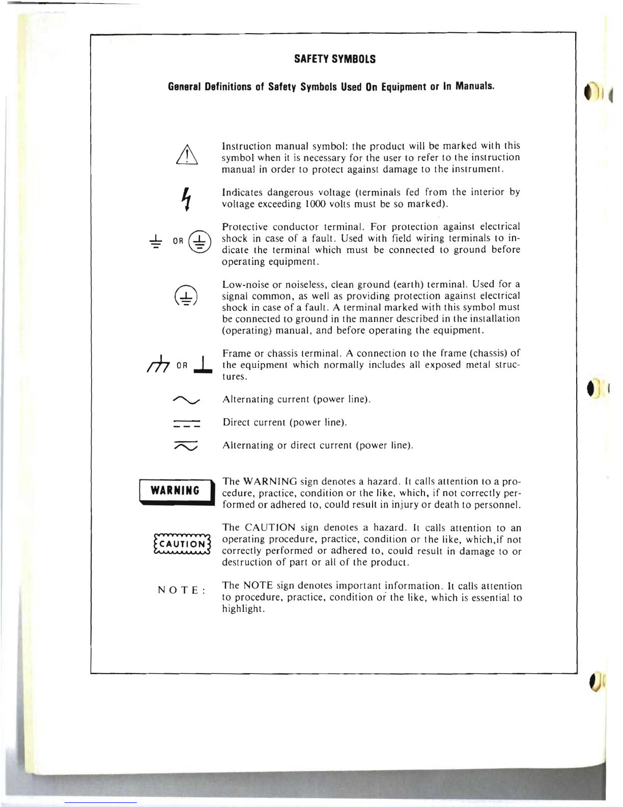
SAFETY
SYMBOLS
General
Definitions
of
Safety
Symbols
Used
On
Equipment
or
In
Manuals.
Instruction manual symbol: the product will be marked with this
symbol when
it
is necessary for the user to refer to the instruction
manual
in
order to protect against damage to the
in
strument.
Indicates dangerous voltage (terminals
fed
from the interior
by
voltage exceeding 1000 volt s must
be
so marked).
Protective conductor terminal. For protection against electrical
OR
~
shock
in
case
of
a fault. Used with field wiring terminals to in-
'0
dicate the terminal which must
be
connected to ground before
operating equipment.
Low-noise or noisele
ss
, clean ground (earth) terminal. Used for a
signal common, as well as providing protection again st electrical
shock
in
case
of
a fault. A terminal marked with this symbol must
be connected to ground
in
the manner described
in
the
in
stallation
(operating) manual , and before operating the equipment.
Frame or chass
is
terminal. A connection to the frame (chassis)
of
rh
OR
..L
the equipment which normally includes all expos
ed
metal struc-
tures.
Alternating current (power line).
Direct current (power line) .
Alternating or direct current (power line).
I The
WARNING
sign denotes a hazard.
It
calls attention to a pro-
WARNING
cedure, practice, condition
or
the like, which, if not correctly per-
"'------
••
formed
or
adhered to, could result
in
injury
or
death to personnel.
The
CAUTION
sign denotes a hazard .
It
calls attention to an
operating procedure, practice, condition or the like , which,if not
correctly performed or adhered to, could result
in
damage to or
destruction
of
part or all
of
the product.
The NOTE sign
denote
s important information .
It
calls attention
NOT
E : to procedure, practice, condition
or
the like, which
is
essential to
highlight.
.-
~
-
.1-
_
.
-~.:..

Model
654A
Section I
SECTION
GENERAL
INFORMATION
1-1_
DESCRIPTlON_
1-2
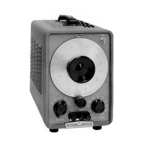
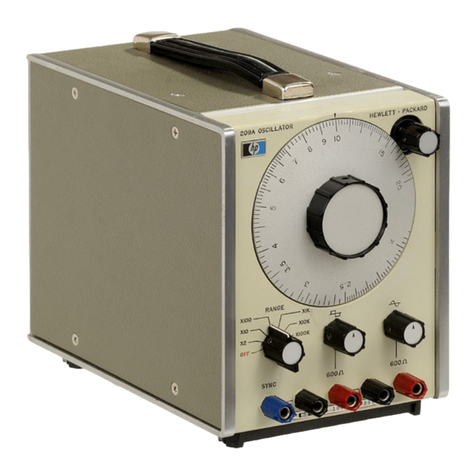
. The Hewlett-Packard Model
654A
Test Oscillator
is
an
ideal
general purpose signal source whenever a flat balanced
or
unbalanced test signal
is
required . Balanced outputs
of
135
ohms, 150 ohms and 600 ohms have many uses
in
the
communications industry. Automatic leveling, together
with the expanded meter, make the
654A
ideally suited to
voltmeter calibration or to test frequency response
of
components during manufacture. The instrument
is
shown
in
Figure I-I and the specifications are listed
in
Table I-I.
General information relating to the instrument
is
listed
in
Table
1-2.
The information
in
Table
1-2
should not be
considered specifications.
1-3. The Model
654A
is
a stable,
low
distortion sine-wave
signal
source with a flat frequency response
of
+/-0.5% over
the frequency range
of
10Hz
to 10
MHz.
The attenuators
allow the signal to be adjusted
in
I
dB
and
10
dB
steps
from +10
dBm
to
-89
dBm, and the front panel
AMPLITUDE control allows a continuous adjustment
in
level
of
+/-1
dB
from the settings shown on the OUfPUT
LEVEL attenuators. The flat frequency response
is
achieved by automatic leveling circuits within the
654A.
1-4.
Five
output impedances are available, selected by a
front panel push-button control: these are 50 and 75 ohms
unbalanced and 135, 150 and 600 ohms balanced. Balance
is
greater than 50
dB
up to I
MHz
and greater than
40
dB
up to 5
MHz
.
1-5.
The meter scale
is
expanded to indicate 0 dBm at
center scale, with a total range
of
+/-1
dBm. The metering
circuit monitors the signal
level
before the attenuators
so
that the meter indication
is
independent
of
the attenuator
settings; the meter indicates the signal level set by the front
panel AMPLITUDE control. The
output
signal
level
into
the load
is
the algebraic sum
of
the meter indication and
the OUTPUT LEVEL attenuator settings.
1-6.
An
additional feature
is
the COUNTER OUTPUT rear
panel
BNC
connector. This allows the Model
654A
frequency to be continuously monitored by
an
electronic
counter without interrupting measurements or affecting
terminal balance .
1-7.
SUPPLIED
ACCESSORIES.
Rack mount kit: -hp- Part
No.
5060-0775.
1-8.
RECOMMENDED
ACCESSORIES.
-hp-
II
048C 50 ohm Feedthrough Termination
-hp-
II
094A
75 ohm Feedthrough Termination
-hp- 11095A
600
ohm Feedthrough Tennination
-hp-11l43A
Balanced
BNC
to Alligator clip cable
1-9.
INSTRUMENT
AND
MANUAL
IDENTIFICATION.
1-10.
Hewlett-Packard uses a two-section serial number.
The first section (prefix) identifies a series
of
instruments.
The last section (suffix) identifies a particular instrument
within the series. If a letter
is
included with the serial
number, it identifies the country
in
which the instrument
was
manufactured.
If
the serial prefix
of
your instrument
differs from the one
on
the title page
of
this manual, a
change sheet
will
be supplied to make this manual
compatible with newer instruments or the backdating
information
in
Appendix C
will
adapt this manual to earlier
instruments.
All
correspondence with Hewlett-Packard
should include the complete serial number.
1-1

Section 1 Model
654A
I
-
B l
floO
S }
r
Figure 1-1. Model
654
A Test Oscillator
Table
I-I.
Specifications
frequency
range: 10
Hz
to
10 MHz in 6 bands.
Frequency
accuracy:
100
Hz
(on
Xl
00
RANGE)
to
5 MHz: +/-2%
10
Hz
to 100 Hz: +/-3 %
5
MHz
to
10
MHz: +/-4%
Level flatness(+IO dBm and 0
dBm):
+/-0.5% referenced
to level
at
I kHz from
10Hz
to 10 MHz for un-
balanced
outputs,
10
Hz
to
5
MHz
for 135
ohm
and
150
ohm
outputs,
and 10
Hz
to I
MHz
for
600
ohm
output.
Attenuator
Range: 99 dB in 10 dB and I dB steps.
Accuracy: +/-1.5%
(0
.
15
dB)
except +/-10%
(I
dB)
at
output
levels below
60
dBm
at
frequencies greater
than
300
kHz.
Amplitude
control:
greater
than
2 dB.
Amplitude
accuracy:
+/-1
% for
90
days (at I kHz,
+ I 0 dBm level with
meter
centered).
Meter tracking: +/-0.05 dB.
Balance
(on
balanced impedances) when measured by the
procedure
given in Paragraph 5-28 : greater
than
50 dB
for frequencies from
10Hz
to I MHz, greater than
40
dB
to
5 MHz .
Distortion
(THD)
10Hz
to
I MHz : greater
than
40
dB below
fu
nda-
mental.
I
MHz
to
10
MHz: greater
than
34
dB below funda-
mental.
Hum
and
noise: greater than
70
dB
down
at
full
output.
Table 1-2. General
Information
Output
impedance:
50
ohm
unbalanced, 75
ohm
un-
balanced, 135
ohm
balanced, 150
ohm
balanced and
600
ohm
balanced.
Output
level:
+11
dBm to -90 dBm, 10 dB and I dB
steps
with adjustable
+/-1
dB
meter
range; calibrated for
each
impedance
.
Meter resolution:
0.02
dB.
1·2
Output
connectors:
BNC . Maximum voltage which can
be
applied
to
the
output:
less
than
+/-3 V peak.
Counter
output:
greater
than
0 .1 V rms
into
50
ohm
,
BNC
connector.
Operating
temperature:
OOC
to
+550 C
(32°F
to
130°F).
Power: 115 V
or
230
V +/ . 10%, 48
Hz
to
66
Hz,
30
W .
1/
1
nominal, 35 W max.
~

I
554A
Model
654A Section
II
SECTION
II
INSTALLATION
2-1.
INTRODUCTION.
2-2.
This section contains information and instructions
necessary for installing and shipping the Model 654A Test
Oscillator. Included are initial inspection procedures, power
and grounding requirements, environmental information,
installation instructions and instructions for repackaging for
shipment.
2·3.
INITIAL
INSPECTION.
2-4.
This instrument
was
carefully inspected both
mechanically and electrically before shipment. It should be
physically free
of
mars or scratches and
in
perfect electrical
order upon receipt. To confirm this, the instrument should
be
inspected for physical damage
in
transi t. Also. check for
supplied accessories, and test the electrical performance
of
the instrument using the proced
ure
outlined
in
Section
Vof
this manual. If there
is
damage or deficiency, see the
warranty on
Page
ii
of
this manual.
2·5.
POWER
REQUIREMENTS.
kHz, 2·6. This instrument
will
operate from either 115 or
230 V ac,
48
Hz
to 66
Hz.
The instrument can easily be
the position
of
the slide switch located
on
the rear panel, so
that the designation appearing on the switch matches the
nominal voltage
of
the power source.
the
o
dB
than
Be/ore applying primary power to the 654A
be slire it is set for the proper
fine
voltage
as
olltlined
in
Paragraph
3-8.
Inda-
2-7.
Power
Cords.
Inda-
2-8.
Figure
2-J
illustrates the standard power plug config-
urations that are
used
throughout the United States and
in
tput. other countries. The
-hp-
part number directly below each
drawing
is
the part number for a 654A power cord
equipped with a power plug
of
1hat configuration. If the
appropriate power cord
is
not included with the instru-
ment , notify the nearest -hp- Sales and Service Office and a
replacement cord will be provided.
2-9.
GROUNDING
REQUIREMENTS.
2-10.
To protect operating personnel, the National Electri-
cal
Manufacturer's Association (NEMA) recommends that
the instrument panel and cabinet
be
grounded. The Model
654A
is
equipped with a three-conductor power cord
which , when plugged into an appropriate receptacle,
grounds the instrument. The offset pin
on
the power plug
is
the ground connection.
8120-1351
8120-1369
8120-1689
STO·8-419~
'UL
LISTED FOR
USE
IN THE UNITED STATES
OF
AMERICA
Figure 2-1.
Power
Cords.
2-11.
INSTALLATION.
2-12. This instrument
is
fully transistorized: therefore no
special cooling
is
required. However, the instrument should
not
be
operated where the ambient temperature
is
outside
the limits specifed
in
Table 1·2.
2-13.
RACK/BENCH
INSTALLATION.
2-14. This instrument
is
initially shipped
as
a bench-type
instrument (unless ordered specifically
as
a rack-type) with
plastic feet and tilt stand
in
place. Conversion
to
a rack-
mounted inst rument can
be
accomplished
by
using the
rack-mounting kit and instruction furnished with
YOUl
inst rumen t.
2-15_
REPACKAGING
FOR
SHIPMENT.
2-16. The following
is
a general guide for repackaging for
shipment. If you have any question, contact your local
-hp-
Sales and Service Office_(See Appendix
at
the back
of
this
manual for office location.)
NOTE
If
the instrument is
to
be shipped to Hewlett-
Packard
for
service or repair, attach a
tag
to
the instrument identifying the owner and
indicating the service
or
repair to be accom-
plished; include the model number and full
serial
number
of
the instrument. In any corre-
spondence, identify the instrument
by
model
number
and serial number.
a.
Place instrument
in
original container if avail-
able. If original container
is
not available, a suit-
able one can
be
purchased from your nearest -hp-
Sales and Service Office.
2-1

Section II Model 654A
If
original conlainer
is
nol used.
b.
Wrap
insirllineni
in
heavy paper or plaslic before
placing
in
In
inner conlainer.
c.
Use
plenly
of
packing malerial
aroLind
all
sides
of
insirLimenl and proieci panel
faces
wilh cardboard
sl
rips.
d.
e.
Place inslrumenl and inner container
in
a heavy
carlon or wooden box
a'nd
seal
will] slrong lape or
i1lel~1
bands. .H I
Mark
shipping conlainer wilh
"DELICATE
INSTRUMENT,"
"FRAGILE"
ele.
2-2
-
11Jj
I L -.
,1,1..
!."

()54A
Model
654A Section Il[
heavy
.a
pe
or
SECTION
III
CATE
OPERATING
INSTRUCTIONS
3-1.
INTRODUCTION.
e.
Adjust the OUTPUT LEVEL attenuators and the
AMPLITUDE control for the desired signal output
3-2
. This section contains instructions and information level. The algebraic sum
of
the meter indication
necessary
for
the operation
of
the 654A Test Oscillator. and the attenuator setting
gives
the power level,
in
[ncluded
in
this section are identification
of
controls, dBm, into a load equal to the impedance selected
indicators and connectors, turn-on procedure, meter by the [MPEDANCE pushbutton. [n Table 3-1, the
mechanical zero adjustment and operating instructions. o dBm and +
10
dBm levels are converted to
voltage
for
each impedance.
3-3.
CONTROlS,lNDICATORS,
AND
CONNECTORS.
3-4
.
All
operating controls, indicators and connectors of
the 654A are identified and described
in
Figure
3-1
.
SWITCH
THE
10
DBM
STEP
ATTENUATOR
DOWN
BEFORE
3-5.
TURN-ON
PROCEDURE.
CONNECT[NG
TO
SENS[T[VE
EQUIPMENT, SUCH
AS
THERMAL
3-6.
OUTPUT METER MECHANICAL
ZERO
CONVERTERS,
SO
AS
TO
PREVENT
ADJUSTMENT
. DAMAGE
FROM
OVERLOAD[NG.
3 -7. The
Model
654A output meter
is
properly Table 3-1. dBm/Voltage Conversion Chart
mechanically zero-set when the meter pointer rests over the
-I
dBm
mark. Zero-set the output meter to obtain
maximum accuracy and mechanical stability
in
the
following manner.
With
LIN
E switch turned off, insert
pOinted object (such
as
tip
of
bal
.1 point pen) into recess on
adjustment wheel, and rotate wheel until meter pointer
rests exactly over
-I
dBm
mark.
3-8.
PRIMARY
POWER
APPLICATION
.
a. Before applying primary power to instrument, set
I
15
or 230
volt
slide switch (S3) to position which
indica tes primary voltage to be used.
f.
Connect the load to the output connectors.
Use
o
dBm
= I m watt into rated load.
Impedance odBm +10 dBm
50
ohm
75 ohm
135
ohm
150 ohm
600 ohm
0.224 V rms
0 .274 V rms
0.367 V
rms
0.387Vrms
0.775 V rms
0.707 V
rms
0.866 V rms
1.162Vrms
1.225 V rms
2.449 V
rms
the UNBAL connector for 50 ohm and
75
ohm
b.
Connect primary power to connector J
I.
Switch loads and both connectors (BAL)
for
135
ohm,
LINE switch
(S
I) to
ON
position : pilot lamp 150 ohm and 600 ohm loads .
(DSI)
will
glow .
3-10.
OPERATING
CHECK.
3-9.
OPERATING
INSTRUCTIONS.
3-11. Before making measurements using the 654A,
a.
Zero
-
set
meter (Paragraph 3-7) and turn perform the following front panel checks to ensure that
instrument on (Paragraph 3-8). your instrument
is
operating correctly.
b.
Set
the FREQUENCY RANGE switch and
a.
Turn AMPLITUDE control until white arrow on
FREQUENCY dial (with VERN[ER) to the knob
is
pointing up; meter should indicate
desired frequency. (Dial reading multiplied by approximately 0 dBm.
range
setting
gives
the frequency
in
Hz_)
b.
Turn
AMPLITUDE
control
extreme
c.
Connect a frequency counter to the rear panel counterclockwise; meter should indicate
-I
dBm or
COUNTER OUTPUT, if desired . less .
d. Select the required output impedance by pressing
c.
Turn AMPLITUDE control extreme clockwise;
the appropriate [MPEDANCE pushbutton. meter should indicate +I
dBm
or greater.
3-\

Section
III
Model 654A
~
'
~4A
fES
T
OSCILlATOR'j;;ffi:;t:t-
-
@
o
rt==f)1
AMF'LI
ruOE
o
FREQUENCY
dial (Cl A/B/C): Varies test
frequency continuously within each frequency
range. Dial reading multiplied by range setting
gives
the out put frequency
in
Hz
of
the 654A.
FREQUENCY RANGE switch (52): Selects one
of
six
frequency multipliers from
Xl
0 to X
1M.
Output Meter
(M
I): Monitors amplitude
of
654A
output prior to OUTPUT LEVEL attenuators.
Algebraic sum
of
meter indication and OUTPUT
LEVEL attenuator setting
gives
output power into
rated load.
Mechanical Zero Adjust: Allows meter to
be
mechanically zeroed, when instrument
is
off.
CD
OUTPUT LEVEL (54): Attenuates 654A output
signal
in
nine steps
of
I dBm each .
o OUTPUT LEVEL (54): Attenuates 654A output
signal
in
nine steps
of
10
dBm each.
CD
UNBAL
out put (14):
BNC
connector provides
an
unbalanced output signal. at impedances
of
50
ohms and
75
ohms.
BAL output (J3 and 14):
BNC
connectors provide
a balanced output signal
at
impedances
of
135
ohms, 150 ohms and 600 ohms.
IMPEDANCE switch (A4S J): Selects required
output impedance
of
instrument; pushbuttons are
interlocked
so
that when one
is
pressed the others
spring out.
@ AMPLITUDE control (R3): Allows adjustment
of
+/-1
dBm
of
output signal amplitude.
®
FREQUENCY
VERNIER: Provides a fine
frequency adjustment for FREQUENCY dial.
@ LINE
ON
switch (51) and Pilot Lamp (DSI):
Switch applies primary power to instrument; pilot
lamp glows to indicate application
of
primary
power.
115
Vor
230 V Slide Switch (53): Sets instrument
® to operate from a primary power source
of
either
I
15
V
ac
or 230 V ac, 48
Hz
to 66
Hz.
FUSE
(FI):
0.4 amp slow blow fuse protects
® instrument from overloads.
COUNTER OUTPUT (12):
BNC
connector
® provides signal output
of
greater than
0.1
V
rms
into a 50 ohm load , at same frequency
as
front
panel out puts.
® Primary Power Connector
(1
I): Connects primary
power to instrument.
Figure 3·1. Location
of
Controls, Indicators and Connectors
3·2

:1654A
uired
IS
are
thers
nt
of
fine
lSI):
pilot
mary
nent
ither
tects
~ctor
rms
'ront
THEORY
OF
4-1.
GENERAL
DESCRIPTION.
4-2. The Model 654A Test Oscillator (see Block Diagram,
Figure 7-1) contains a
Wien
Bridge Frequency Adjustable
Oscillator
(10Hz
to
10
MHz)
followed by a Buffer
Amplifier and a Balanced Amplifier with a single ended
input and balanced output. The output
of
the Balanced
Amplifier
is
a leveled, sinusoidal signal; this signal passes
through Balanced Attenuators and a Balance and Unbalance
Impedance Switch (output impedance switching network)
to
the front panel output connectors.
4-3
. An
Average
Responding Detector monitors the
output
from
the Balanced Amplifier to provide two
dc
currents
(proportional to the
signal
level); one current flows to the
meter circuits and the other to the Amplitude Control
Integrator.
Au
tomatic leveling
of
the 654A
signal
is
achieved by means
of
the Amplitude Control Integrator
which compares the current from the
Average
Detector
with the current
from
an Amplitude Current Reference to
regulate the current through the lamp
of
a photosensitive
control device (A2DSVI). The lamp controls the imped-
ance
of
a resistive divider at the inpu t
of
the Buffer
Amplifier
so
as
to maintain a constant
output
level
from
the Balanced Amplifier. The
output
level
attenuators
provide attenuation
in
10
dB
and I
dB
steps
at
the output
connectors and a front panel AMPLITUDE control gives
2
dB
of
continuous output
level
adjustment by varying the
current from the Amplitude Current Reference.
4-4. The current from the Average Detector which flows
to
the meter circuits
is
divided into two parts : a fixed amount
of
current (approximately 1.25 rna)
flows
into the Meter
Offset Current Reference and the remainder
flows
to the
meter.
In
this way the meter
is
offset
so
that
it
indicates
only over the range
of
-I
dBm to +I dBm. The current
flowing into the Meter Offset Current Reference
is
held
con~tan't
by
the Meter Differential Amplifier which clamps
the Input of the current reference to a virtual ground.
4-5.
A Counter Emitter Follower provides isolation
between
th
e oscillator circuit and the rear panel COUNTER
OUTPUT.
Regulated Power Suppli
es
provide the +
31
V
and -
26
V reqUired to operate the 654A.
4-6.
CIRCUIT
DESCRIPTION_
4-7.
OSCILLATOR
CIRCUIT
(Schematic
No
.
1,
Figure
7-2)
4-
8.
The frequency adjustable Oscillator drives the Buffer
Model
654A Section
IV
SECTION
IV
OPERATION
Amplifier with a stable sine
wave
at a frequency determined
by the setting
of
the FREQUENCY RANGE switch and the
FREQUENCY dial. The circuit
is
a
Wien
Bridge Oscillator
which
has
a standard, frequency selective,
RC
leg
and a
resistance
leg
modified by the addition
of
a variable
impedance (A2CR I and A2CR2). A2Q26 and
A2Q
I
through A2Q6 comprises the amplifier section and
A2Q7
is
a peak detector which provides negative feedback to the
bridge
for
leveling. Two types
of
feedback are used; positive
feedback from the frequency selective network drives the
base
of
A2Q3 through the source follower A2QI, and
negative feedback from the resistive side
of
the bridge
drives the base
of
A2Q2. A2Q2 and A2Q3 form a
differential amplifier. Only
at
the selected frequency does
the positive feedback overcome the negative feedback to
sustain oscillations.
4-9. The six frequency ranges are selected by means
of
the
RC
networks mounted on the FREQUENCY RANGE
switch (S2); continuous adjustment
of
the frequency on
each range
is
accomplished by rotating the FREQUENCY
dial, which controls the setting
of
the tuner capacitors
CI
A,
CI
Band
CI
C.
The signal from the amplifier out put (from
A2Q5 and A2Q6)
is
developed across the
RC
network
of
the bridge; at the selected frequency, where Xc = R (Figure
4-1), the positive feedback to the base
of
A2Q3
has
the
correct phase and sufficient amplitude to sustain
oscillations. The high input impedance
of
the
field
effect
transistor
(A2QI)
prevents the amplifier from loading the
frequency determining
leg
of
the bridge; the feedback
prOVided
by A2Q26 prevents any changes
in
the parameters
of
A2QI from affecting the frequency response
of
the
amplifier. The difference between the positive and negative
FREQUENCY
0.5
/
'\
/
/ \ ////
/
////
\
/
/'
/'
"
7/
/
//
",,/
~
LAG
0.4
0.3
_F_
p_
PHASE
F
0.1
LEAD
F
p;
POSITIVE
FEEDBACK
TO
AMPLIFIER
RATIO--
PHASE
-----
F ;
FEEDBACK
TO
RC
NETWORK
6!54A-A-187
9
Figure
4-1
.
RC
Network Characteristics
4-1

4-2
Section
IV
feedback signals
is
amplified by the differential amplifier
(A2Q2 and A2Q3) and applied, through emitter follower
A2Q4, to the complementary symmetry pair A2QS and
A2 Q
6.
The very
low
output impedance
of
the
complementary pair acts
as
a constant voltage source
for
the Buffer Amplifier and
also
allows feedback to
be
applied
to the bridge without loading the output
of
the oscillator.
A2QS
and A2Q6 are forward biased through A2CR7 and
A2CRS
so
as
to conduct slightly when
no
signal
is
applied;
this eliminates crossover distortion
of
the output signal.
4-10 . A2Q7 acts
as
a peak detector. Part
of
the oscillator
signal
is
superimposed on a negative bias at the base
of
A2Q7; A2Q7 conducts only when the positive peaks
of
the
signal overcome the negative bias. The negative dc output
of
A2Q7
is
filtered by A2C2, A2C3 and A2C4 and used to
bias
the diodes A2CRI and A2CR2
so
as
to vary the
impedance of the negative feedback side
of
the bridge to
control the amplitude
of
oscillations.
A2RS
is
switched into
the circuit on the
XI
00 through
XI
M ranges and
A2CS
on
the
XIO
through
XI
K ranges
for
extra filtering. A2CR3
limits any reverse voltage transients across the polarized
capacitors
A2C3
, A2C4 and A2CS. A2R9*
is
selected to
draw current from the bridge
so
as
to balance the current
through A2CR I and A2CR2 and improve distortion
in
the
output signal.
4·11.
BUFFER
AMPLIFIER.
(Schematic
1)
4·12 . The BtJffer Amplifier (A2QS through A2Q I0)
provides isolation between the oscillator and the Balanced
Amplifier and
is
also
used
as
the point at which the 6S4A
signal
is
leveled.
A2QS
and A2Q9 form a differential
amplifier whose output, from the
co
llector
of
A2Q9,
is
amplified by A2QlO and
fed
to the Balanced Amplifier.
Part
of
the signal output from
A2Q
lOis applied
as
negative
feedback through A2R39 to the base
of
A2QS
to stabilize
the amplifier gain over its
10Hz
to
10
MHz
frequency
range. The signal from the oscillator
is
divided down at the
input to the Buffer Amplifier by a resistive divider
consisting
of
A2R33 and the
resi
stive element
of
the
photosensitive resistor (A2DSV
I).
The resistance
of
the
resistive element
is
determined by the current through the
lamp, which
is
controlled by the Automatic Leveling
Circuits (Paragraph 4-19 and following) . The signal
level
at
the input of the Buffer Amplifier varies with changes
in
the
resistance of the photosensitive resistor to control the
level
of
the 6S4A output signal.
4·13.
COUNTER
EMITTER
FOLLOWER.
(Schematic
1)
4-14. The Counter Emitter Follower
(A3Ql)
serves
as
isolation between the Oscillator circuit, and the rear panel
COUNTER OUTPUT (12). The output frequency
is
the
same
as
the Variable Test Oscillator frequency .
Signal
amplitude at the COUNTER OUTPUT
is
approximately
0.1
V
rms
into a
50
ohm load .
4-15.
BALANCEO
AMPLIFIER.
(Schematic
2,
Figure
7-3)
Model6S4A
4-16. The single-ended sinusoidal output from the Buffer
Amplifier
is
amplified and converted into a balanced
signal
\\
in
the Balanced Amplifier. The Amplifier consists
of
three'll
cascaded differen tial amplifiers (A2Q II through
A2Q
16)
and two complementary symmetry pairs (A2Q IS, A2QI9
and A2Q20, A2Q21). The balanced
output
signal from the
complementary symmetry pairs
is
developed across
summing resistors A2R74 and A2R7S and then applied
through A2R76 and C9, and through A2R77 and
CIO
to
the attenuators (S4). The input sinusoidal signal at the base
of
A2QII
is
converted into two signals
of
equal amplitude,
but
ISOo
out
of
phase, taken from the collectors of A2QII
and
A2Q
12. The two signals then follow parallel paths,
while maintaining the
ISO
o phase relationship, through the
Balanced Amplifier. One signal path
is
through
A2QII,
A2Q
13
and A2Q
15
to the complementary symmetry pair
A2QIS and A2Q19 ; the other signal path is through
A2Q12, A2QI4 and A2QI6 to complementary symmetry
pair A2Q20 and A2Q21. The complementary pairs are
biased through diodes A2CRIS, A2CRI6 and A2CRI7,
A2CRIS
so
that the transistors conduct slightly when
no
signal
is
applied; this eliminates crossover distortion
of
the
signal at the
output
of
the Balanced Amplifier.
4-17. The gain
of
the Balanced Amplifier
is
stabilized by
means
of
negative feedback. A2RSI couples the output
signal from the top
of
A2
R74 back to the base
of
A2Q
II
and A2RS3 couples the opposite signal from the bottom
end
of
A2R7S back to the base
of
A2Q12. Note that the
~
r
application
of
feedback together with the
high
gain
of
th
e
~
.
Amplifier and the very low signal source impedance (from '
the Buffer Amplifier) causes the Balanced Amplifier
to
function
as
an operational amplifier with differential input
and output;
as
a result , the overall gain
of
the Balanced
Amplifier
is
determined by the ratio
of
A2RSI to A2R44
and A2RS3 to A2RS4. Capacitors
A2C1S
and
A2C1S
improve the
high
frequency r
es
ponse
of
the feedback paths.
4-IS. To maintain proper balance
of
the output signal, the
junction
of
summing resistors A2R74 and
A2
R7S
is
held at
virtual ground by means
of
negative feedback to the third
differential amplifier (A2QIS, A2QI6). The differential
pair A2Q22 and A2Q23 compares the voltage at the
junction of A2R74 and A2R7S with ground (the base of
A2Q23
is
connected directly to ground). Any signal
unbalance or common mode signal across the two resistors
moves their junction away from ground; this voltage at the
junction
is
amplified by A2Q22 and A2Q23 and applied to
the base
of
A2Q
17
to change its coll
ec
tor current.
A2Q
17
is
the source
of
current
for
A2Q
15
and
A2Q
16
so
that the
change
in
current through them
will
be
such
as
to
re
store
the balance between the two sinusoidal signals and return
the junction
of
A2R74 and A2R7S back to ground. A2C32
is
adjusted for equal signal voltage across A2R74 and
A2R7S. A2R47, A2C16, A2C23, A2C26 , A2C27,
A2C2S
and A2C29
all
serve
as
frequency shaping elements
to
improve the frequency response and to insure stability of
the Balanced Amplifier over its frequency range
of
10Hz
to
10
MHz.

lei
654A
e Buffer
ed
signal
of
three I
A2Q16)
. A2QI9
~
rom
the
across
applied
I
CIO
to
the base
Iplitude,
, A2QIl
!I
paths,
)ugh the
A2QII,
!try pair
through
'mmetry
lairs
are
l2CR17,
...,hen
no
n
of
the
lized
by
output
. A2QII
bottom
that the
n
of
the
:e (from
lifier to
ial
input
lalanced
A2R44
A2C18
k paths.
~al,
the
;
held
at
he
third
ferential
at the
base
of
f
signal
resistors
~e
at
the
'plied
to
A2QI7
that the
restore
i return
A2C32
74 and
A2C28
lents to
lility
of
o
Hz
to
Model
654A
4-19.
AMPLITUDE
CONTROL
AND
AUTOIVlATIC
LEVELING
CONTROL.
4-20. The amplitude
of
the balanced sine
wave
Signal
from
the Balanced Amplifter
is
independent
of
the Attenuator
settings but can be varied over a 2
dB
range by the front
panel AMPLITUDE control (Schematic 2). The Automatic
Leveling Circuit (ALC) consists
of
the Average Detector,
the Amplitude Control Integrator, and the Amplitude
Current Reference (varied by the AMPLITUDE control).
The
Average
Detector monitors the output
of
the Balanced
Amplifier and produces a dc current proportional to the
amplitude
of
the Balanced Amplifier signal. The Amplitude
Control Integrator compares this dc current with a current
of
opposite polarity from the Amplitude Current
Reference; any difference
in
magnitude between the
current from the Average Detector and the reference
current
is
used
to apply negative feedback to the
photosensitive resistor at the input
of
the Buffer Amplifier
until the output
of
the Balanced Amplifier
is
at the level
where the two currents are equal. The output
of
the
Balanced Amplifier
is
at the required
level
when the current
from the Average Detector
is
equal to the reference current.
4-21. AVERAGE DETECTOR. (Schematic 2)
4-22. The detector monitors the output
of
the Balanced
Amplifier. A2Q24 and A2Q25 form a high
gain
amplifier
which
is
a current source for the detector (A2CR21 and
A2CR22).
A2CR21
supplies the metering circuits with a
positive dc current and A2CR22 supplies the
ALC
circuits
with a negative dc current. These currents are equal
in
ampl.itude to each other and proportional to the amplitude
of
the Balanced Amplifier output signal. A2Q24 and
A2Q25
(together with the components connected to the
base
of
A2Q25) form essentially one transistor with high
gain, high output impedance and very
low
output
capacitance; these factors together with the 'bootstrap'
capacitor A2C42 account for the amplifier's effectiveness
as
a current source over a wide frequency and temperature
range.
A2C43 (Freq. Response)
is
adjusted
for
flat
frequency response
of
the detector circuit.
4-23
. AMPLITUDE CURRENT REFERENCE.
(Schematic 2)
4-24. Zener Diode A I CR8 maintains a constant voltage
across
R3
(front-panel AMPLITUDE control) and A2R91
in
series, the Amplitude Control Integrator ma.intains
essentially 0 Vdc at the output
of
the current reference (at
the
base
of
A3Q6): thus, for any
given
setting
of
R3, there
IS
a
fixed
voltage drop across
A3Rl9
and
A3
R20 and a
fixed
amount
of
current flows from the Amplitude Current
Reference.
When
the setting
of
the AMPLITUDE control
~R3)
is
changed , the voltage drop across
A3
R
19
and A3R20
IS
changed ; this sets a new fixed value
of
current
flOWing
towards the base
of
A3Q6 .
4-25. AMPLITUDE CONTROL INTEGRA TOR.
(Schematic 2)
4-26. The
ci
rcuit consis
ts
of
A3Q6 through A3Q9 and
Section
IV
associated circuitry, including the lamp
of
the photo-
sensitive resistor A2DSV I (Schematic
I)
.
A3Q6
and A3Q7
form a differential amplifier; any change
in
output from the
collector
of
A3Q7
is
amplified by A3Q8 and applied to the
base
of
A3Q9 to change the current through the lamp
of
the photosensitive resistor (A2DSVI). Changes
in
lamp
current change the impedance
of
the voltage divider at the
input
of
the Buffer Amplifier (paragraph 4-12), thus
changing the sine wave signal
level
through the Buffer
Amplifier and the Balanced Amplifier. The
dc
current from
the Average Detector
is
compared,
at
the base
of
A3Q6,
with the current from the Amplitude Current Reference.
In
the differential pair (A3Q6, A3Q7) the base
of
A3Q7
is
connected directly to ground; therefore, as long
as
the base
of A3Q6
is
held at 0 Vdc, there will
be
no
change
in
output
from the collector
of
A3Q7. The amplitude
of
the positive
current flowing from the Amplitude Current Reference
is
ftxed; the amplitude
of
the negative current flowing from
the Average Detector depends
on
the level
of
signal at the
output
of
the Balanced Amplifier. These currents are
summed
at
the base
of
A3Q6 . The difference current flows
into the base
of
A3Q6. The amplitude
of
the base current
is
set
by
the AMPLITUDE CAL. adjustment and the
AMPLI-
TUDE control.
As
long as this current
level
is
not changed
by a variation
in
the Average Detector output, there will be
no
change
in
current through the lamp
of
the photo-
sensitive resistor; thus the
ac
signal level at the
ou
tput
of
the Balanced Amplifier will be constant.
In
this condition,
the
ALC
loop
is
in
the "quiescent" state and the output
of
the 654A
is
at the required level.
4-27. Suppose that the output
level
of
the Balanced
Amplifier
now
changes for some reason (e.
g.
the frequency
of
the
Wien
Bridge Oscillator
is
changed); then the
Amplitude Control Integrator
will
act to return the signal
back to
it
s original level
in
the
follOWing
manner:
a.
The negative current from the Average Detector
(A2CR22)
will
change proportionally with the
change
in
ac
signal level. This current flowing into
the summing node at the base
of
A3Q6
diminishes
the positive current amplitude thus decreasing the
base current to A3Q6. TIlls,
in
turn, begins to shut
off
the transistor.
b.
The output
of
the Amplitude Control Integrator
changes
in
response to the new input
so
as to
change the
ac
signal
level
into the Buffer Ampli-
fier.
TIlls
will
be
in
such a direction
as
to
return
the Balanced Amplifier
ac
ou
tput back to the
level
where the
nega
live
dc
current from the Average
Detector
is
again equal to its quiescent value.
In
this way the 654A
ou
tput signal
is
maintained at a
constant level.
4-28. To manually control the 654A output
level
over the
2
dBm
range, the AMPLITUDE control setting
is
changed;
this changes the current from the Amplitude Current
Reference thus changing the base current to A3Q6. The
Amplitude Control Integrator now acts
as
before to change
the Balanced Amplfier
ac
output
level
until the current
4-3

4-4
Section
IV
differential at the base
of
A3Q6
is
equal to its quiscent
value. The
ALC
circuit contains an integrator for fast
response without overshoot and without sacrificing the
ability to reject ripple superimposed
on
the curr.ent from
the Average Detector. S2C14
is
switched
in
parallel with
A3Cl0
on
the XIO RANGE for required response
of
the
Amplitude Control Integrator
at
low frequencies.
4·29
.
METER
CIRCUITS.
(Schematic
2)
4·30. The meter circuits consist
of
the Meter Differential
Amplifier, the Meter Offset Current Reference and the
Meter.
As
explained
in
Paragraph 4·22, the Average
Detector (A2CR2] and A2CR22) monitors the Balanced
Amplifier output and produces two
dc
currents, equal
in
amplitude but opposite in polarity, proportional to the
Balanced Amplifier
output.
The positive output
of
the
Average Detector (from
A2CR2l)
flows to the meter
circuits. A fixed part
of
this curren t flows into the Meter
Offset Current Reference and the remainder flows through
the Meter and
its
shunt resistors
A3Rl7
and A3RIS. The
Meter
(M])
is
calibrated to indicate center scale when the
654A output into rated load (the attenuators set
at
0 dBm)
is
0 dBm. The total range
of
the meter scale
is
+/·1
dBm so
that when the Meter indicates·] dBm, no current
is
flowing
through the Meter and
all
of
the current from the Average
Detector
is
flowing through the Meter Offset Current
Reference circuit.
4·3 I. The action
of
the Meter Offset Current Reference
and
the Meter Differential Amplifier
is
very similar to the
action
of
the Amplitude Current Reference and the
Amplitude Control Integrator (described
in
Paragraphs 4·22
through 4-25) . Apart from a
few
minor differences the
circuits are identical.
4-32. The Meter Offset Current Reference consists
of
A3R6, A3R7, A3RS, A3R9 and A3CR2. A3CR2
is
a
special temperature compensated Zener diode which
maintains a constant voltage across A3R7 and A3RS
in
series. Thus. the current flowing into the circuit
is
determined essentially by the voltage across A3R9 . This
current must always
be
a fixed amount
so
as
to offset the
Meter scale correctly ; therefore, the voltage across
A3
R9
must always
be
fixed; this
is
achieved by means
of
the
Meter Differential Amplifier. The Meter Differential
Amplifier consists
of
A3Q2 through A3Q5. A3Q2 and
A3Q3 form a differential pair; since the base
of
A3Q3
is
connected directly to ground, the base
of
A3Q2
will
be
held at a virtual ground. Any difference between the two
bases causes
an
output change from the collector
of
A3Q3
which
is
amplified by A3Q4 and applied to A3Q5 so
as
to
return the base
of
A3Q2 back to virtual ground. One side
of
A3R9
is
connected
to
the base
of
A3Q2, which
is
clamped
to a virtual ground; the other side
of
A3R9
is
connected to
a constant voltage point (set by A3R7); thus the voltage
across A3R9
is
held constant
as
required, and the Meter
Offset Current Reference always takes a fixed amount
of
the current from the Average Detector to offset the Meter.
A3C5 serves to improve the frequency stability
of
the
Model 654A
Meter Differential Amplifier. A3C6
is
connected across the
Meter to damp the meter movement, and A3C7
is
switched
in paraUel with A3C6 on the XIO RANGE so
as
to
further
improve damping
of
the Meter at very low frequencies.
1\
4·33.
ATTENUATO
RS.
(Schematic
3)
4·34. The balanced sine wave signal, developed across
A2R74 and A2R75
in
the Balanced Amplifier,
is
fed
through A2R76 and C9, and through A2R77 and
CIO
to
the Attenuators (S4). The attenuator assembly (S4) consists
of
four attenuators; a ]
dB
step and a
10
dB
step attenuator
connected
in
series
for
each
of
the two
halves
of
the
balanced signal. Each attenuator consists
of
four resistive
networks which are switched
in
various combinations to
give
the required attenuation. The front panel controls
consist
of
two concentric rotary knobs labelled OUTPUT
LEVEL dBm; the outer control, marked
in
10
dB steps,
controls
both
of
the
10
dB
step attenuators simultaneously;
the inner control, marked
in
]
dB
steps, controls both
of
the 1
dB
step attenuators simultaneously.
4·35
.
IMPEDANCE
SELECTOR.
(Schematic
3)
4-36. The front panel IMPEDANCE switch
(A4S])
selects
the reqUired
output
impedance
of
the 654A. The
impedance networks and the switching connect ions are
shown on schematic 3; the switch connections are shown
with the 50 ohm UNBAL
button
pushed.
In
the
BAL
mode, both front panel
output
connectors,
13
and 14,are
used;
in
the UNBAL mode, only 14
is
used. ,r
4·37.
REGULATED
POWER
SUPPLY.
4-38 . The regulated power supply provides
all
dc
voltaged
required
by
the 654A Test Oscillator circuits. The power
supply consists
of
a
+31
V
and·
26
V series regulated
supply. Each power supply is protected
by
current limiting
and foldback current limiting .
4·39 . Tile +3] V and -26 V power supplies are functially
identical. Both
use
operational amplifiers for output voltage
error amplification . AI R40 adjusts the
+3
I V supply
voltage
and
A I
R41
adjusts the .
26
V supply voltage .
4-40. Conventional current limiting
is
used
in
both supplies
to
limit the
output
curren I
to
approximately 300
mA
o
Foldback current limiting further limits the
output
current
if the
output
voltage
is
pulled below approximately
16
V
by a malfunction
in
the 654A circuitry. A direct short to
ground
of
either supply
will
result
in
an
output current
of
approximately
10
mA
as
shown
in
Figure 4-2.
441.
Figure 4·3
is
a simplified schematic
of
the current
limiting circuitry used
in
the 654A power supplies.
The
Current Limiting Transistor A I Q4(
+)
or AI Q7( - )
is
a
variable shunt to the series regulator drive current.
It
is
first
switched on
by
the voltage drop across tile Currellt
LimIt
Sensing Resistor when the power supply output current
reaches approximately 300
mAo
The power supply
will
remain
in
this Conventional Current Limit condition until
the output current decreases allowing the supply to return "
to normal operation,
Of
until the power supply output
~J
voltage drops below the Foldback Reference (]6.2V).

llo4ITEA
----
--,
I
SEAlES
REGULAT~
~
'I
OKJO(
SWrTCH
I
I
FOLDBACI(
L
__
~~tfE
SHUNT
CUAAENT
DAIVE CURRENT
L.
___
____
.....
__
el654A
Model
654A
:ross
the
witched
, further
.es.
~V~
_______
R~E~~~~~TE~D~~~T.~G~E
________
~
I across
,
is
fed
cia to
consists
:enuator
of
the
resistive
tions
to
controls
IUTPUT
B steps, IOOmA
200mA
300m
A
~
f-
3
10V
OUTPUT CURRENT
leously;
both
of
Figure
4-2.
Regulated
Power
Supply
Output
Voltage
vs
Current.
) selects
A.
The
ions are
~
shown
he
BAL
j J4, are
voltaged
e power
ogulated
limiting
JIlctially
. voltage
supply
voltage.
supplies
00
rnA.
curren t
Iy
16
V
short to
Hent
of
current
ies. The
- )
is
a
I t
is
first
It
Limit
current
ply
will
on until
J return
output
16.2V).
OONvENnCIIIAL
CURRENT
LIMIT
i552A-B-4314
Sectiull
II
If the latter occurs, the Diode Switch
is
effectively closed
and the power supply goes into a Foldback Current Limit
condition.
In
this condition the Current Limiting Transistor
is
controlled
by
tile power supply
outpu
t Voltage.
As
tile
output voltage decreases, the shunt current
is
increased.
UNA£OULATEO
DC
~~~f~
==;;-'
OONVENTlONAl
CUARENT
LIMITER
1-
-iii~T~~i~\~-----
1
'
I'
\ :
f"
R(
:j,L!L
A
T"[C
f--
i
---.-wY-..---
-+--
-""""
~
WJl
~
J
T
i 32<
I ,
L
__
__
____
_ _
_____
...J
r-----
I
Figure
4-3.
Simplified
Schematic
of
Current
Limiting
Circuitry
4-5

WARNING
I
Maintenance
described
herein
is
performed
with
power
supplied
to
the
instrument,
and
pro
-
tective
covers
removed.
Such
maintenance
should
be
performed
only
by
service-trained
personnel
who
are
aware
of
the
hazards
in-
volved
(for
example,
fire
and
electrical
shock).
Where
maintenance
can
be
performed
without
power
applied,
the
power
should
be
removed.

Model
654A Section V
SECTION
V
MAINTENANCE
5-1.
INTRODUCTION.
5-2.
This section contains maintenance and service
information for the
-hp-
Model
654A Test Oscillator.
Included are performance checks and adjustment and
calibration procedures.
5-3.
Tabl
e
5-1
lists the equipment required to properly
maintain the
Model
654A. If the recommended model
is
not available. any instrument that has specifications equal
to, or better than . the required specifications may
be
used.
5-4.
PERFORMANCE
CHECKS.
5-5
The performance checks are in-cabinet tests (except
where noted) to cOlllpare the performance
of
the
Mod
el
654A with the specifications
given
in
Table I-I. These
checks
Illay
be
used
for incoming inspection. periodic
maintenance and
for
performance checks after a repair. The
Performance Check Test card
at
the end
of
Section V may
be
cut
out,
and used
as
a permanent record of the
instrument's performance during incoming inspection.
It
is
recommended t hat performance checks and, if necessary.
calibration
be
performed every 90 days.
5·
6.
FREOUE'NCY
CHECKS.
5-7.
FREQUENCY RANGE CHECK.
a.
Connect
all
electronic counter to the 654A rear
panel COUNTER OUTPUT.
b. Set the 654A controls
as
follows :
FREQUENCY RANGE
......
. .
...
XIO
FREQUENCY
dial.
. . .
...
Extreme clockwise
c. The counter should indicate a period average
of
lOOms
or
greater. verifying a frequency
of
10Hz,
or less, at the lower end
of
the frequency range.
d.
Set the FREQUENCY RANGE switch to XIM and
FREQUENCY
dial
to
its
extreme
counter-clockwise postiton. The counter should
indicate a frequency
of
10MHz, or greater,
verifying a frequency of at least 10MHz at the
upper end
of
the frequency range.
e. Perform the Frequency Adjustments (Paragraphs
5-47 through 5-57) if the tolerances are not met.
5-8. FREQUENCY ACCURACY CHECK.
a.
Connect
an
electronic counter to the 654A rear
panel COUNTER OUTPUT.
b.
Set the 654A controls
as
follows:
FREQUENCY RANGE
..
...
. .
..........
XIO
FREQUENCY dial
........................
1
c. Verify frequency accuracy using the settings and
tolerances
given
in
Table 5
-2.
Use
t
he
period
average setting on the counter for frequencies
below I k
Hz
and
use
the frequency setting for
frequencies above I kHz .
d. Perform the frequency adjustments (Paragraphs
547
through 5-57) if the tolerances are not met.
5·9.
AMPLITUDE
ACCURACY
CHECKS.
(See also Table 3-1, Page 3-1).
5-10 .
SO
UNBAL AMPLITUDE ACCURACY.
a.
Connect the equipment
as
shown
in
Figure 5-1.
Use
the 50 ohm Feedthrough termination which
should
be
connected directly to the 654A output
connector.
b.
Set the 654A controls
as
follows:
FREQUENCY
dial..
..
....
..
I
FREQUENCY RANGE . , . , .
XI
K
OUTPUT LEVEL dBm
........
. .
".
. + I 0,0
IMPEDANCE
.....
....
..
..
.......
50 UNBAL
AMPLITUDE
..
. .
...
..
.. .. ..
Adjust
for
OdBm
on 654A meter.
c.
The ilC voltmcter iIHJication should
be
betwecn
.7000 V
rms
allLl
7
1.:11
V
rnl
S verifying
an
abso-
lute
level
of+
10
dBnl. +/
-1'
,"
d.
If the tolerances are not met perform
th
e Meter
Tracking and Amplitude Control Adjustments
of
Pmagraphs 5-58 through 5-60.
5-11. 75 UNBAL AMPLITUDE ACCURACY.
a.
Perform the procedure
of
Paragraph 5-10 except:
instep
a.
Use
the
75
ohm feedthrough
termination;
5-1

5-
2
Section V
Model
654A
Table 5-1. Required Test Equipment
INSTRUMENT
TYPE REQUIRED CHARACTERISTICS RECOMMENDED MODEL
Frequency
10
.00Hz to 1000MHz
El
ec
tronic -hp- Mude l 5245L
Countcr P
er
iod : 1.000 ms tu 100
.Oms
.
El
ec
tron
ic
Counter.
Ran
ge:
.9999V
rill
s and 9.999V
rms
full sca
le
.
-lIp-
,"Iudel J
--lS
OB
Vllllillcicr
AC
Di
gil
al
Mulli/\lI1cli
l)
n
Mel
cr
wil
li
OPT
00
I
A
cc
ur acy:
al
least . I 'If
of
reading
at
I kHz .
Wav
e
Fr
eq
uency Range I
MHz
III
22MHz.
-hr
· Model H05-31
2A
Analy
zc
r
Mu
st
be
cu mpatib
le
w
it
h Tr
ack
in
g O
sc
illat or.
Wa
ve
Analyzer.
(N
ute: the
H0
5-3
I
2A
is
required on
ly
for
di
stortion checks,
otherwise a standard -hp- 3 I
2A
can
be
used .)
Must
be
cap
abl
e
of
ex
pandi ng wave analyzer
Tr
ac
kin g
-hp-
Model 3
13A
Os
cillator metcr indi
ca
tion to resolve 0.05dB. T racki
ng
O
sc
illat o
r.
Distortion Sen
si
tivit
y:
gr
eater than 46dB.
-hp-
Modcl 333A
Analyzer
Di
sturti un
Fr
eq
uency range · 10Hz to 600kHz.
Di
stortion Analyzer.
-hp- Model 46 I A Gene
ral
F requcncy range : I kHz to 10MHz.
Amplifier Gain: 40dB .
Purpose Amplifi er.
-hp- Model
400E
Voltage ra
nge
I .00
mV
rm
s to I .
OOV
rms
Frequ
en
cy
ra
ng
e:
10Hz to
10MH
z.
AC
Vo
ll
nlcter
AC
Vo ltmcle
r.
(dB
sca
le
s referenced
to
I
mW
int o
600
o
hm
s).
Ran
ge:
IOuV to 10mV .
-hp-
Mod
el 4 I
9A
V
ul
t meter
DC
Null
DC
Null
Vo ltmetcr.
A
cc
uracy : +/-2
'7<
of
full
sc
al
e.
-
hp-
Model 4
27
A
Input Impedan
ce
10
mego hms.
Range 0. 1
V to 100V .
DC
Voltmete r
Multi-F unc tion Mete
r.
Oscill
os
cope
Sen
si
ti
vity : 5mV!cm. -hp-
Model
180 A
Bandwidt h :
dc
to 50MH
z.
Oscilloscope with 1
80
I A
and I 820A plug-ins.
Fe
ed
thruu
gh
Feed-Thru
Termina
ti
ng
Resi
stan c
e:
(a) -hp- Model 1I04SC
(3
) 50 u
hm
s +
/-25'
i[
Re
s
i
s
t
~
lnc
e
(b)
75
ohms
+/
-.25
(;
~
(b) -
hr
-
Mod
el 1I094A
All
cn
uat ors
Fr
equ e
ncy
r
an
gl'
:
10H
z to
10Mf-I
z (with known
acc urac y
at
10kHz_
300kJlz and 10MHz)
Al
te nuation
rall
gc:
VHF
Altenu ators
(a)
-hp-
Mod
el
35
5C
(a) 9dB
in
IdB steps .
(b) -hp- Model
35
5D
(b) 90dB
in
I
OdB
steps
Thef1l1al
Fr
equency range :
10H
z
to
1
0MH
z.
Cunvert e
rs
Input
at
least +IOdBm into rat
ed
input impedan ce.
Inp
ut
impedance :
(a) 50 o hms_ unbalanced.
(b)
75
o
hm
s, unbalanced .
( c)
13
5 ohm
s,
bal
an
ce
d.
(d) 150 ohms, balanced .
(
e)
60
0 ohm
s,
balan
ce
d.
Thermal Convert e
rs
(a) -hp Model
1I0
50A
(b) -hp - Mo
del
HOI
-I 1050A
(c) -
hp-
Model
HI
I
-I
1050A
(d)
-hp-
Model H
12-1
1050A
(
e)
-hp- Model HIO-11050A
Bl"C
to
Bin
ding
P
os
t Adap(er
-hp-
Mod
el 10110A
(2
required)
R
es
istors . l iS
W,
metal
film
.
(a)
75
o hm
s_
.25
% (t
wo
requ
ire
d) .
(b)
13
5 ohms , . I 'It
(f
o
ur
required).
(d
300 oh m
s,
. I r
ic
(two required) .
-hp-
Part
No:
0698-6262
0698-7364
0698 -6295
Not
e.
Th e fu
ll
ow
in
g items
ar
e not com m
erC
ially a
va
ilable
bUI
ca
n be easily co
nsl
ruclcu . Icfe r to the figures
hsted
fo
r schemalics and part, lis
ts
.
DC
Refere
nc
e
Su
ppl
y
Fi
gu
re
54
No t
e:
The foll ow
in
g a
re
useful optional item
s.
1)
.Jumper
ca
bl
e,
8
in,
-hp -Part No. 10502-600 1
(2 required,
se
e Para gra
ph
5-30a)
75 uhm
[()
50
oh
m Illlpcu a
ncc
Co
nvcnCf
B
ala
n
ce
B
ox
Fi
gure 5-7
Fi
g
ur
e
5-9
2 )Sin e
-Wa
ve
Signal Generator : may
be
r
eq
uir
ed
for
troubt
es
hoo tln g
(Refer to
Par
ag
raph s 5
-7
9 and 5
-8
3.)
10MHz Low-
Pass
Filtcr
ligureS-12
Other manuals for 654A
1
Table of contents
Other HP Power Tools manuals
Popular Power Tools manuals by other brands

Pro's Kit
Pro's Kit SS-331B user manual

BLACK DECKER
BLACK DECKER HD565 Original instructions

Swisstech
Swisstech Mega-Max 15-in-1 quick start guide

FLORABEST
FLORABEST FSG 85 B1 translation of original operation manual

Silvercrest
Silvercrest SEAS 20 A1 operating instructions

RAPIDTOOL
RAPIDTOOL RT-60 user guide