R3
8Bridge-tied load (BTL)
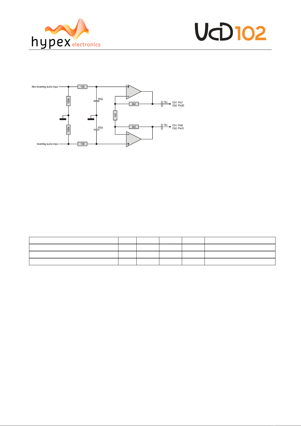
This two channel amplifier can be utilized in Bridge Tied Load configuration. This is especially useful
for high impedance loads. In a bridge-tied load configuration, channel 1 is driving one side of a load
and channel 2 is driving the other side of the load. The signal input of channel 2 is the inverted
signal input of channel 1. Note that this does not affect the phase of the signal. A BTL configuration
results in double the voltage swing across the load compared to a single-ended configuration where
one side of the load is tied to an amplifier and the other side to ground.
In the graphical representation above, the BTL principle is depicted. By inverting the signal input of the second
channel, the output voltage amplitude is doubled. Please note that the negative (GND) output terminals are tied
together. On the UcD102 module, this is already implemented in the design and therefor these pins can be left
unconnected.
In a bridge-tied load configuration, the load impedance which each amplifier channel ‘sees’ is half
the characteristic impedance of the connected speaker. Therefor the minimum load in BTL
configuration is 4Ω, however, we recommend to use only a BTL configuration with a load of 8Ωor
higher.
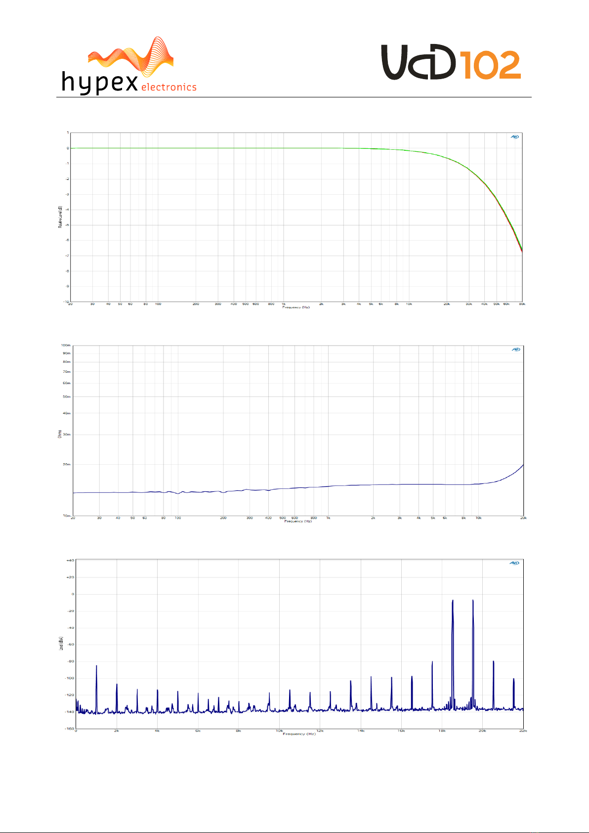
1KHz, THD=1%,
Bridge-tied load (BTL)
Loudspeaker impedance
range
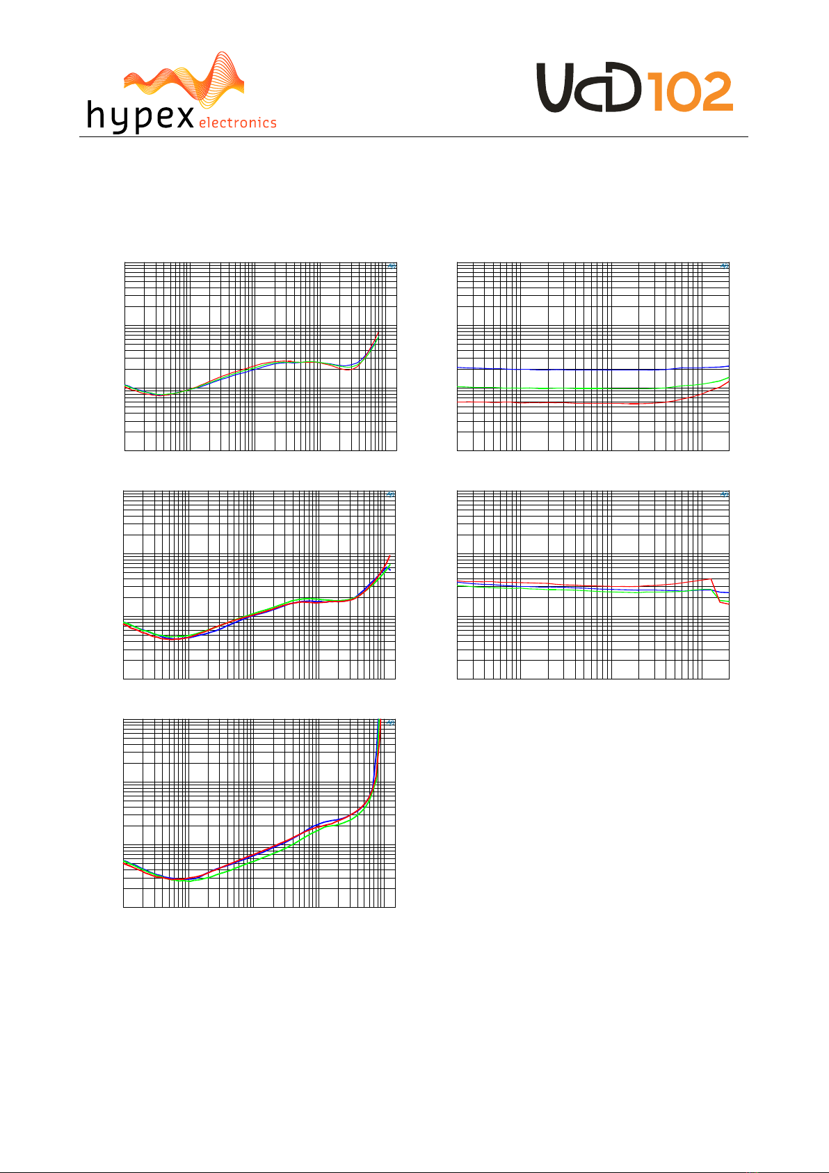
8.1 Typical Performance Graphs BTL
THD+N vs. power at 100Hz (blue), 1kHz (green) and 6kHz (red) (BTL - 4Ω).
THD+N vs. power at 100Hz (blue), 1kHz (green) and 6kHz (red) (BTL - 8Ω).
Ls1+
Ls1-
Ls2+
Ls2-
Ground tie
Speaker connection Channel
inversion
In1+
In1-
In2+
In2-
input
Bal+
Bal-
source
Bal-
Bal+
Source connection Speaker connection
The input signal must be anti-parallelconnected
to the module's channel.
This can be done physically, but one can also
choose to invert the signal in a DSP.
0.001
1
0.002
0.005
0.01
0.02
0.05
0.1
0.2
0.5
10m 20020m 50m 100m 200m 500m 1 2 5 10 20 50 100
0.001
1
0.002
0.005
0.01
0.02
0.05
0.1
0.2
0.5
10m 30020m 50m 100m 200m 500m 1 2 5 10 20 50 100 200