Icom IC-2720H User manual

DUAL BAND FM TRANSCEIVER
i2720H
SERVICE
MANUAL

INTRODUCTION
This service manual describes the latest service information
for the IC-2720H DUAL BAND FM TRANSCEIVER at the
time of publication
DANGER
NEVER connect the transceiver to an AC outlet or to a DC
power supply that uses more than 16 V. This will ruin the
transceiver.
DO NOT expose the transceiver to rain, snow or any liquids.
DO NOT reverse the polarities of the power supply when
connecting the transceiver.
DO NOT apply an RF signal of more than 20 dBm (100 mW)
to the antenna connector. This could damage the transceiv-
er’s front end.
ORDERING PARTS
Be sure to include the following four points when ordering
replacement parts:
1. 10-digit order numbers
2. Component part number and name
3. Equipment model name and unit name
4. Quantity required
<SAMPLE ORDER>
1110004310 S.IC M62352GP IC-2720H MAIN UNIT 5 pieces
8810009610 Screw FH M2.6×6 ZK IC-2720H bottom cover 10 pieces
Addresses are provided on the inside back cover for your
convenience.
REPAIR NOTES
1. Make sure a problem is internal before disassembling the
transceiver.
2. DO NOT open the transceiver until the transceiver is
disconnected from its power source.
3. DO NOT force any of the variable components. Turn
them slowly and smoothly.
4. DO NOT short any circuits or electronic parts. An insu-
lated tuning tool MUST be used for all adjustments.
5. DO NOT keep power ON for a long time when the trans-
ceiver is defective.
6. DO NOT transmit power into a signal generator or a
sweep generator.
7. ALWAYS connect a 50 dB to 60 dB attenuator between
the transceiver and a deviation meter or spectrum ana-
lyzer when using such test equipment.
8. READ the instructions of test equipment thoroughly
before connecting equipment to the transceiver.
To upgrade quality, any electrical or mechanical parts and
internal circuits are subject to change without notice or
obligation.
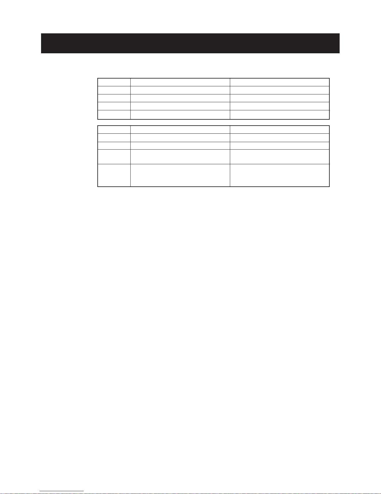
MODEL
IC-2720H
VERSION
U.S.A.
Korea
S.E.Asia
Export
SYMBOL
USA
KOR
SEA
EXP

TABLE OF CONTENTS
SECTION 1 SPECIFICATIONS
SECTION 2 INSIDE VIEWS
SECTION 3 DISASSEMBLY INSTRUCTIONS
SECTION 4 CIRCUIT DESCRIPTION
4 - 1 RECEIVER CIRCUITS . . . . . . . . . . . . . . . . . . . . . . . . . . . . . . . . . . . . . . . . . . . . . . . . . . . . . . . . . . . .4 - 1
4 - 2 TRANSMITTER CIRCUITS . . . . . . . . . . . . . . . . . . . . . . . . . . . . . . . . . . . . . . . . . . . . . . . . . . . . . . . . .4 - 5
4 - 3 PLL CIRCUITS . . . . . . . . . . . . . . . . . . . . . . . . . . . . . . . . . . . . . . . . . . . . . . . . . . . . . . . . . . . . . . . . . .4 - 6
4 - 4 POWER SUPPLY CIRCUITS . . . . . . . . . . . . . . . . . . . . . . . . . . . . . . . . . . . . . . . . . . . . . . . . . . . . . . .4 - 8
4 - 5 CPU PORT ALLOCATIONS . . . . . . . . . . . . . . . . . . . . . . . . . . . . . . . . . . . . . . . . . . . . . . . . . . . . . . .4 - 10
SECTION 5 PARTS LIST
SECTION 6 MECHANICAL PARTS AND DISASSEMBLY
SECTION 7 SEMI-CONDUCTOR INFORMATION
SECTION 8 BOARD LAYOUTS
8 - 1 CONTROL UNIT . . . . . . . . . . . . . . . . . . . . . . . . . . . . . . . . . . . . . . . . . . . . . . . . . . . . . . . . . . . . . . . . 8 - 1
8 - 2 MAIN UNIT . . . . . . . . . . . . . . . . . . . . . . . . . . . . . . . . . . . . . . . . . . . . . . . . . . . . . . . . . . . . . . . . . . . . .8 - 3
8 - 3 VCO UNIT . . . . . . . . . . . . . . . . . . . . . . . . . . . . . . . . . . . . . . . . . . . . . . . . . . . . . . . . . . . . . . . . . . . . .8 - 5
SECTION 9 BLOCK DIAGRAM
SECTION 10 VOLTAGE DIAGRAMS
10 - 1 CONTROL UNIT . . . . . . . . . . . . . . . . . . . . . . . . . . . . . . . . . . . . . . . . . . . . . . . . . . . . . . . . . . . . . . . 10 - 1
10 - 2 MAIN AND VCO UNITS . . . . . . . . . . . . . . . . . . . . . . . . . . . . . . . . . . . . . . . . . . . . . . . . . . . . . . . . . .10 - 2

1 - 1
SECTION 1 SPECIFICATIONS
All stated specifications are subject to change without notice or obligation.
MGENERAL
• Frequency range :
LEFT SIDE
RIGHT SIDE
*1Guaranteed 144.000 – 146.000 MHz only, *2Guaranteed 144.000 – 148.000 MHz only,
*3Guaranteed 430.000 – 440.000 MHz only; *4Guaranteed 440.000 – 450.000 MHz only
*5Not guaranteed range
• Mode : FM, AM (AM range is 118.0 – 135.995 MHz and Rx only for [USA] and [EXP].)
• Nomber of memory channel : 212 (including 2 call channels and 10 scan edges)
• Usable temperature range : –10˚C to +60˚C; +14˚F to +140˚F
• Frequency resolution : 5, 10, 12.5, 15, 20, 25, 30 and 50 kHz
• Frequency stability : ±10 ppm (–10˚C to +60˚C; +14˚F to +140˚F)
• Power supply requirement : 13.8 V DC ±15 % (negative ground)
• Current drain (at 13.8 V DC) : Receive Standby (squelched) 1.2 A
Max. audio output 1.8 A
Transmit at VHF 50 W/UHF 35 W 12.0 A/11.0 A
• Antenna connector : SO-239 (50 Ω)
• DATA connector : Mini DIN 6 pin
• Dimensions : Controller 140(W)×50(H)×27(D) mm; 51⁄2(W)×131⁄32(H)×11⁄16(D) inch
(projections not included) Main unit 140(W)×40(H)×187(D) mm; 51⁄2(W)×19⁄16(H)×73⁄8(D) inch
• Weight : Controller 150 g; 5.29 oz
Main unit 1.4 kg; 3.0 lb
MTRANSMITTER
• Output power : VHF 50 W/25 W/5 W (selectable)
UHF 35 W/25 W/5 W (selectable)
• Modulation system : Variable reactance frequency
• Maximum frequency deviation: ±5.0 kHz
• Spurious emissions : Less than –60 dB
• Microphone connector : 8-pin modular jack (600 Ω)
MRECEIVER
• Receive system : Double-conversion superheterodyne
• Intermediate frequency : 1st IF 38.85 MHz/46.05 MHz
(Left/right side band) 2nd IF 450 kHz/455 kHz
• Sensitivity : Less than 0.18 µV (at 12 dB SINAD)
• Squelch sensitivity : Less than 0.13 µV (at threshold)
• Selectivity : More than 12 kHz/–6 dB (Wide); More than 6 kHz/–6 dB (Narrow)
Less than 30 kHz/–60 dB (Wide); Less than 20 kHz/–60 dB (Narrow)
• Spurious and image rejection : More than 60 dB
• Audio output power (at 13.8 V) : More than 2.4 W at 10% distortion with an 8 Ωload
• External speaker connector : 2-conductor 3.5(d) mm (1⁄8")/8 Ω
VERSION
[KOR]
[SEA]
[EXP]
[USA]
RX (MHz)
144.000–146.000, 430.000–440.000
136.000–179.995*2, 430.000–440.000
118.000–549.995*2
118.000–549.995*2, *4
TX (MHz)
144.000–146.000, 430.000–440.000
140.000–150.000*2, 430.000–440.000
136.000–174.000*2, 400.000–479.000*3
144.000–148.000, 430.000–450.000*4
VERSION
[KOR]
[SEA]
[EXP]
[USA]
RX (MHz)
144.000–146.000, 430.000–440.000
136.000–173.995*2, 430.000–440.000
118.000–179.995*2, 375.000–549.995*3
810.000–999.990*5
118.000–174.000*2, 375.000–549.995*4,
810.000–824.000*5, 849.000–869.000*5,
894.000–999.990*5
TX (MHz)
144.000–146.000, 430.000–440.000
140.000–150.000*2, 430.000–440.000
136.000–174.000*2, 400.000–479.000*3
144.000–148.000, 430.000–450.000*4

SECTION 2 INSIDE VIEWS
2 - 1
• CONTROL UNIT (TOP VIEW)
Key back light
(DS14, DS15: LN1371G) LCD back light
DS1-3, DS7-9: SML-010MT
DS4-6, DS10-12: SML-020MLT
Key back light
(DS16, DS17: LN1371G)
Key back light
(DS15, DS18: LN1371G)
Key back light
(DS14, DS15: LN1371G) LCD back light
DS1-3, DS7-9: SML-010MT
DS4-6, DS10-12: SML-020MLT
Key back light
(DS16, DS17: LN1371G)
Key back light
(DS15, DS18: LN1371G)
• MAIN UNIT (TOP VIEW)
VHF low-pass filter
Power amplifier
(Q27: RD70HVF1)
Drive amplifier
(Q25: 2SK3075)
Main CPU
(IC2013: HD64F2144AFA20)
VCO unit
AF amplifier
(IC2012: LA4445)
VHF low-pass filter
Power amplifier
(Q27: RD70HVF1)
Drive amplifier
(Q25: 2SK3075)
Main CPU
(IC2013: HD64F2144AFA20)
VCO unit
AF amplifier
(IC2012: LA4445)
VHF RX Pre amplifier
(Q33: 3SK272)
UHF RX Pre amplifier
(Q24: 3SK274)
Drive amplifier
(Q25: 2SK3075)
TX pre-amplifier
(Q16: 2SK2854)

• CONTROL UNIT (BOTTOM VIEW)
Dimmer
+8V regurator
(Q1: 2SC4116)
+5V regurator
(IC3:TA78L05F)
Sub CPU
(IC4: HD6473847RH)
Reset IC
(IC2: S-80945CLMC)
Data comparator
(IC1:TA75S01F)
Mic amplifier
IC5:TA75S558F
Q15: 2SC4116
Dimmer circuit
(Q6
-
Q13: 2SC4116)
+8V regurator
Q1: 2SC4116
Q3: 2SA1586
D1: MA8091
+5V regurator
(IC3:TA78L05F)
Control unit CPU
(IC4: HD6473847RH)
Reset IC
(IC2: S-80945CLMC)
Data comparator
(IC1:TA75S01F, D2: MA8047)
Mic amplifier
IC5:TA75S558F
Q15: 2SC4116
• MAIN UNIT (BOTTOM VIEW)
D/A converter
(IC1: M62352GP)
+8V regurator
(IC2003:TA7808F)
Mic amplifier
(IC2014:TA75S558F)
Analog switch
IC2007: BU4066BCFV
IC2010: BU4066BCFV
D/A converter
(IC1: M62352GP) UHF low-pass filter circuit
Ceramic bandpass filters
FI1000: CFWM450E
FI1001: CFWS450HT
FI1002: CFWM455E
APC amplifier
(IC2:TA75S01F)
PLL circuit
+5V regurator
(IC2002:TA7805F)
+8V regurator
(IC2003:TA7808F)
Mic amplifier
(IC2014:TA75S558F)
Analog switch
IC2007: BU4066BCFV
IC2008: BU4066BCFV
IC2010: BU4066BCFV
FM IF IC
IC1001:TA31136FN
IC1004:TA31136FN
2 - 2

SECTION 3 DISASSEMBLY INSTRUCTIONS
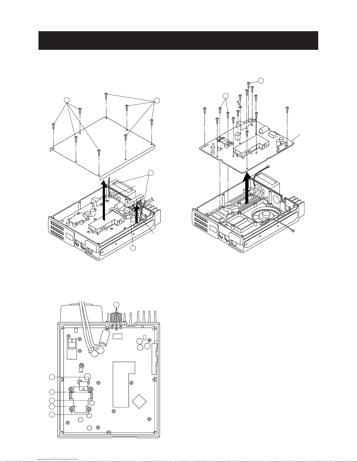
• Removing the MAIN unit
➀Unscrew 8 screws A, and remove the cover.
➁Disconnect two cables Bfrom J1 and J2007.
➂Remove the clip c.
AA
B
C
J2007
J1
G
F
G
F
H
E
MAIN UNIT
J
I
➃Unsolder 3 points E.
➄Unscrew 4 screws F.
➅Unsolder 4 points G, and remove the cover H.
➆Unscrew 2 screws I.
➇Unscrew 12 screws J, and remove MAIN unit.
3 - 1

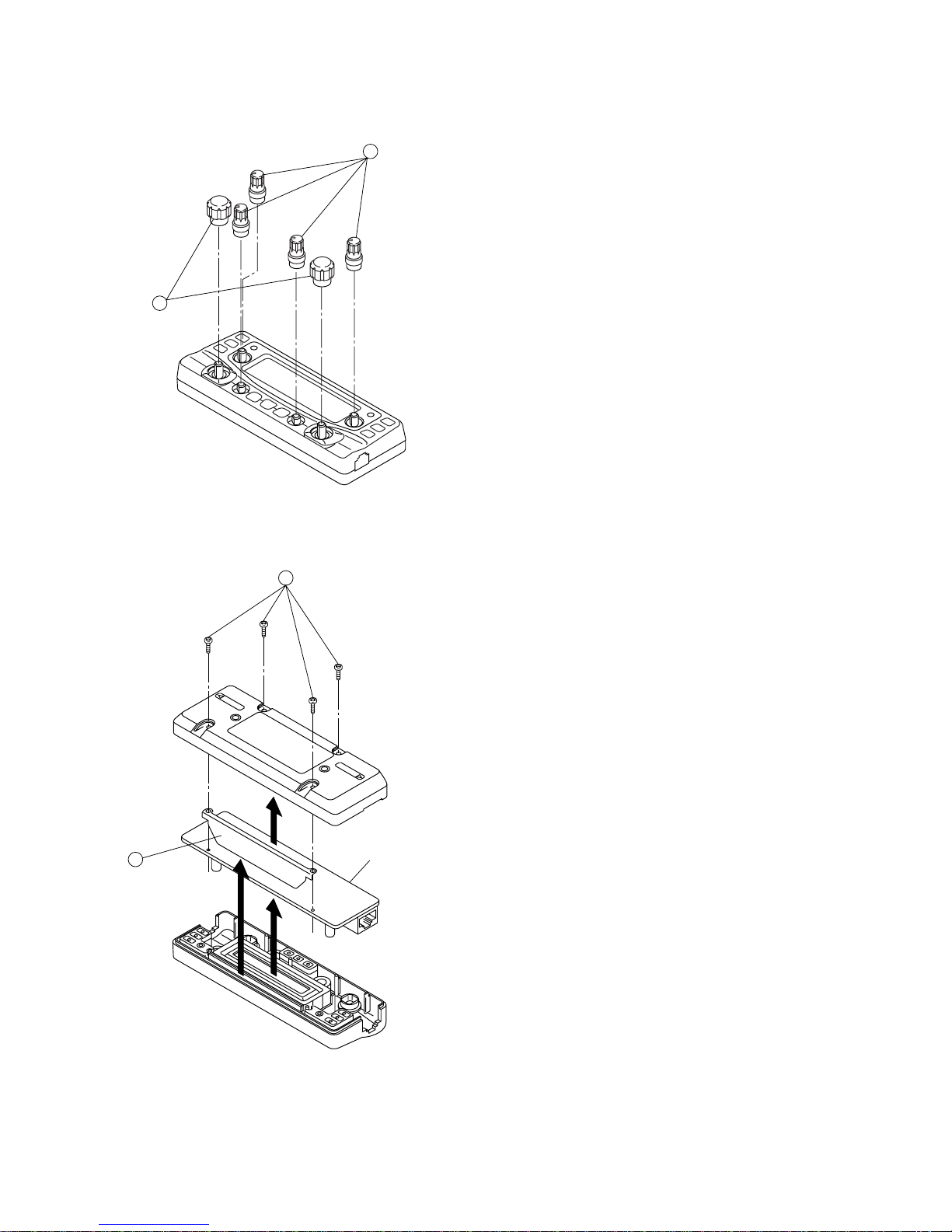
• Removing the CONTROL unit
➀Remove 6 knobs A.
A
A
➁Unscrew 4 screws B, and remove the cover.
➂Remove the plate C, and remove CONTROL unit.
B
CCONTROL UNIT
3 - 2

4 - 1
SECTION 4 CIRCUIT DESCRIPTION
4-1 RECEIVER CIRCUITS
4-1-1 TRIPLEXER AND RX BAND SWITCHING
CIRCUITS (MAIN UNIT)
The transceiver has a triplexer (low-pass and high-pass fil-
ters) on the first stage from the antenna connector to sepa-
rate the signals into VHF and UHF signals. The RF signals
from the antenna connector are applied to the tripler or RX
band swtich circuits.
• RF SIGNALS V-V (118 MHz–180 MHz), U-V (136
MHz–174 MHz)
The V-V and U-V RF signals from the antenna connector
pass through the low-pass filter (L76, L77, L80, C205, C209,
C242, C243, C264), and then applied to the TX/RX switching
circuit (D42, D46, D52, D67, D2049). The filtered signals are
amplified at the pre-amplifier (Q33), and are applied to the
left side or right side displayed RX circuits.
• RF SIGNALS U-U, V-U2 (375 MHz–550 MHz)
The U-U and V-U2 RF signals from the antenna connector
pass through the high-pass filter (L78, L81, C206, C210,
C213, C265), and then applied to the TX/RX switching circuit
(D55, D64, D65, D2050) via the SWR detector (D50, D58).
The filtered signals are amplified at the pre-amplifier (Q24),
and are applied to the left side or right side displayed RX cir-
cuits.
• RF SIGNALS U-U3 (810 MHz–1000 MHz)
The U-U3 RF signals from the antenna connector pass
through the two low-pass filters (L76, L77, L80, C205, C209,
C242, C243, C264, L87, L88, C266–C268), and are then
applied to the RX band swtiching circuit (D2061). The filtered
signals are amplified at the RF amplifier (Q18), and are
applied to the right side displayed RX circuits.
• RF SIGNALS V220 (174 MHz–260 MHz), V-U1 (225
MHz–375 MHz)
The V220 and V-U1 RF signals from the antenna connector
are applied to the RX band swtiching circuit (Q34, D66, RL1),
and are applied to the left side displayed RX circuit.
4-1-2 RF CIRCUIT FOR LEFT SIDE DISPLAY
(MAIN UNIT)
• RF SIGNALS V-V (118 MHz–180 MHz)
The amplified signals are applied to the RF amplifier (Q29)
after being passed through the attenuator (D59) and band-
pass filter (D47, D53). The signals are applied to the RX
band switching circuit (D28) via the another bandpass filter
(D32, D39) to supress the unwanted signals.
• RF SIGNALS V220 (174 MHz–260 MHz)
The signals are applied to the RF amplifier (Q31) after being
passed through the RX band switching circuit (D62) and
bandpass filter (D51). The amplified signals are applied to
the RX band switching circuit (D28) via the another bandpass
filter (D34) to supress the unwanted signals and attenuator
(R195–R197).
• RF SIGNALS V-U1 (225 MHz–375 MHz)
The signals are applied to the RF amplifier (Q32) after being
passed through the RX band switching circuit (D63) and
bandpass filter (D49). The amplified signals are applied to
the RX band switching circuit (D31) via the attenuator
(R198–R200) and another bandpass filter (D35) to supress
the unwanted signals.
• RF SIGNALS V-U2 (375 MHz–550 MHz)
The amplified signals are applied to the RF amplifier (Q20)
after being passed through the attenuator (D25) and band-
pass filter (D23, D73). The signals are applied to the RX
band switching circuit (D9) via the another bandpass filter
(D13, D17) to supress the unwanted signals.
BPF BPF
ANTENNA
1st mixer
(IC1005)
1st LO
to 2nd mixer
circuit
ATT
RX
SW RF PRE
BPF BPF ATT
RX
SW RF PRE
BPF BPF
ATT
RX
SW RX
SW
RX
SW
RF
BPF BPF
ATT
RX
SW RX
SW
RF
D59Q29
V-V (118 MHz—174 MHz)
V220 (174 MHz—260 MHz)
V-U1 (225 MHz—375 MHz)
V-U2 (375 MHz—550 MHz)
D28 D32, D39 D47, D53
D62Q31D30 D34 D51
D63Q32D31 D35 D49
Q33
Q34, D66,
RL1
D25Q20D9 D13, D17 D23, D73 Q24
• RF CIRCUIT FOR LEFT SIDE DISPLAY

4 - 2
The signals from the RX band swtiching circuits are then
applied to the left side displayed 1st mixer circuit (IC1005, pin
6).
4-1-3 1ST MIXER AND 1ST IF CIRCUIT FOR LEFT
SIDE DISPLAY (MAIN UNIT)
The 1st mixer circuit converts the received RF signals to a
fixed frequency of the 1st IF signal with a PLL output fre-
quency. By changing the PLL frequency, only the desired fre-
quency will pass through the bandpass filter at the next stage
of 1st mixer circuit.
The RF signals are mixed with 1st LO signals at the 1st mixer
(IC1005) to produce a 38.85 MHz 1st IF signal. The 1st IF
signal is output from pin 1, and passed through the crystal
bandpass filter (FI1003) to suppress unwanted harmonic
components. The filtered signal is amplified at the IF amplifi-
er (Q1040) after being passed through the limiter circuit
(D1021). The amplified signal is applied to the 2nd mixer cir-
cuit (IC1001).
4-1-4 2ND IF AND DEMODULATOR CIRCUITS FOR
LEFT SIDE DISPLAY (MAIN UNIT)
The 2nd mixer circuit converts the 1st IF signal to a 2nd IF
signal. A double conversion superheterodyne system (which
converts receive signal twice) improves the image rejection
ratio and obtains stable receiver gain.
The FM IC IC (IC1001) contains the 2nd mixer, limiter and
noise amplifiers, quadrature detector, S-meter detector,
active filter circuits, etc. A 2nd LO signal (38.4 MHz) is pro-
duced at the PLL circuit by dividing it’s reference frequency.
The 38.85 MHz 1st IF signal from the IF amplifier (Q1040) is
applied to the 2nd mixer section of the FM IF IC (IC1001, pin
16), and is mixed with the 2nd LO signal (38.4 MHz) to be
converted to a 450 kHz 2nd IF signal.
The 2nd IF signal is applied to the each demodulator circuits
by AM or FM mode.
• FM MODE
The 2nd IF signal is output from the FM IF IC (IC1001, pin 3)
and passes through the ceramic bandpass filter (FI1001).
The filtered signal is fed back to the IC, and amplified at the
limiter amplifier section (pin 5), then demodulated intoAF sig-
nals at the quadrature detector section (pins 10, 11). The
detected AF signals are output from pin 9 and are applied to
the AF circuit via the AM/FM selector circuit (IC2015, pins 7,
1).
• AM MODE
The 2nd IF signal is output from the FM IF IC (IC1001, pin 3)
and passes through the ceramic bandpass filter (FI1000).
The filtered signal is applied to the AM detector circuit
(Q1017) to convert into AF signals, and then amplified at the
Q1014 (pins 5, 1). The amplifiedAF signals are applied to the
AF circuit via the AM/FM selector circuit (IC2015, pins 6, 1).
4-1-5 AF AMPLIFIER CIRCUIT FOR LEFT SIDE
DISPLAY (MAIN UNIT)
TheAF amplifier circuit amplifies the demodulatedAF signals
to drive a speaker.
The AF signals pass through the AF mute switch (Q1010),
and are then applied to the electric volume control circuit
(IC2011, pin 1) as “VAFO” signal after being passed through
the low-pass filter (Q1007). The level controlled AF signals
are output from pin 2, and are then applied to the AF power
amplifier (IC2012, pin 2) via the “VOUT1” signal. The power
amplifiedAF signals are applied to the internal speaker (SP1)
via the [EXT SP] jack (J2005).
The electronic volume control circuit controls AF gain, there-
fore, theAF output level is according to the [VOL] setting and
also the squelch conditions.
4-1-6 NOISE SQUELCH CIRCUIT FOR LEFT SIDE
DISPLAY (MAIN UNIT)
• NOISE SQUELCH
A noise squelch circuit cuts out AF signals when no RF sig-
nal is received. By detecting noise components in theAF sig-
nal, the squelch circuit switches the AF mute switch.
16
Limiter
amp.
2nd IF filter
450 kHz
PLL IC
IC1
X1
12.8 MHz
38.4 MHz
RSSI
IC1001 TA31136F
13 1st IF (38.85 MHz)
from Q1040
"L_RSSI" signal to the CPU
(IC2013, pin 33)
11
10
9
875322
VCO UNIT
1
Active
filter
FI1001
FI1000
Noise
detector
FM
detector Noise
comp.
"L_SQL" signal to the CPU
(IC2013, pin 40)
12
R1124
R1291
C1108
C1100
R1108
C1078
C1085 C1084
C1097
AM
DET. IF
amp.
C1069
R1092
R1109
R1114
L_R5
X1001
FM or WFM AF signal
to AM/FM selector
AM AF signal
to AM/FM selector
Mixer
2nd
Q1049 from Q1013
3
C1271
• 2ND IF AND DEMODULATOR CIRCUIT FOR LEFT SIDE DISPLAY

4 - 3
A portion of the AF signals from the FM IF IC (IC1001, pin 9)
are applied to the active filter section (IC1001, pin 8). The
active filter section amplifies and filters noise components.
The filtered signals are applied to the noise detector section
and output from the IC1001 (pin 14) as the “L_SQL” signal.
The “L_SQL” signal from IC1001 (pin 14) is applied to the
CPU (IC2013, pin 40). The CPU analyzes the noise condition
and outputs the “L_DET_MUTE” signal to theAF mute switch
(Q1010).
• TONE SQUELCH
The tone squelch circuit detects AF signals and opens the
squelch only when receiving a signal containing a matching
subaudible tone (CTCSS). When tone squelch is in use, and
a signal with a mismatched or no subaudible tone is
received, the tone squelch circuit mutes the AF signals even
when noise squelch is open.
A portion of the AF signals from the FM IF IC (IC1001, pin 9)
passes through the low-pass filter (Q1003) to remove AF
(voice) signals. The filtered signal is applied to the CTCSS
decoder which is inside the CPU (IC2013, pin 41) via the
“L_DTCS_IN” line to control the AF mute switch (Q1010).
4-1-7 RF CIRCUIT FOR RIGHT SIDE DISPLAY
(MAIN UNIT)
• RF SIGNALS U-V (136 MHz–174 MHz)
The amplified signals are applied to the RF amplifier (Q30)
after being passed through the attenuator (D60) and band-
pass filter (D48, D54). The signals are applied to the RX
band switching circuit (D29) via the another bandpass filter
(D33, D40) to supress the unwanted signals.
• RF SIGNALS U-U3 (810 MHz–1000 MHz)
The signals are applied to the RF amplifier (Q18) after being
passed through the RX band switching circuit (D2061). The
amplified signals pass through the attenuator (L19, C20,
C46, C51, R178–R180) and high-pass filter (L20, C278,
C279), and are then applied to the another RF amplifier
(Q35) again. The signals pass through the attenuator (L10,
C15, C280, R183–R185) and RX bamd switching circuit
(D11).
• RF SIGNALS V-U2 (375 MHz–550 MHz)
The amplified signals are applied to the RF amplifier (Q19)
after being passed through the attenuator (D24) and band-
pass filter (D22, D72). The signals are applied to the RX
band switching circuit (D8) via the another bandpass filter
(D12, D16) to supress the unwanted signals.
The signals from the RX band swtiching circuits are then
applied to the right side displayed 1st mixer circuit (IC1006,
pin 6).
4-1-8 1ST MIXER AND 1ST IF CIRCUIT FOR RIGHT
SIDE DISPLAY (MAIN UNIT)
The 1st mixer circuit converts the received RF signals to a
fixed frequency of the 1st IF signal with a PLL output fre-
quency. By changing the PLL frequency, only the desired fre-
quency will pass through the bandpass filter at the next stage
of 1st mixer circuit.
The RF signals are mixed with 1st LO signals at the 1st mixer
(IC1006) to produce a 46.05 MHz 1st IF signal. The 1st IF
signal is output from pin 1, and passed through the crystal
bandpass filter (FI1004) to suppress unwanted harmonic
components. The filtered signal is amplified at the IF amplifi-
er (Q1041) after being passed through the limiter circuit
(D1022). The amplified signal is applied to the 2nd mixer cir-
cuit (IC1004).
4-1-9 2ND IF AND DEMODULATOR CIRCUITS FOR
RIGHT SIDE DISPLAY (MAIN UNIT)
The 2nd mixer circuit converts the 1st IF signal to a 2nd IF
signal. A double conversion superheterodyne system (which
converts receive signal twice) improves the image rejection
ratio and obtains stable receiver gain.
The FM IC IC (IC1004) contains the 2nd mixer, limiter and
noise amplifiers, quadrature detector, S-meter detector,
active filter circuits, etc.A 2nd LO signal (45.595 MHz) is pro-
duced at the PLL circuit by dividing it’s reference frequency.
BPF BPF
ANTENNA
1st mixer
(IC1006)
1st LO
to 2nd mixer
circuit
ATT
RX
SW RF PRE
BPF BPF ATT
RX
SW RF PRE
HPF
ATT ATT
RX
SW RX
SW
D60Q30
U-V (136 MHz 174 MHz)
U-U3 (810 MHz 1000 MHz)
V-U2 (375 MHz 550 MHz)
D29 D33, D40 D48, D54
D2061
RF
Q35
RF
Q18D11
Q33
D24Q19D8 D12, D16 D22, D72 Q24
• RF CIRCUIT FOR RIGHT SIDE DISPLAY

4 - 4
The 46.05 MHz 1st IF signal from the IF amplifier (Q1041) is
applied to the 2nd mixer section of the FM IF IC (IC1004, pin
16), and is mixed with the 2nd LO signal (45.595 MHz) to be
converted to a 455 kHz 2nd IF signal.
The 2nd IF signal is applied to the each demodulator circuits
by AM or FM mode.
• FM MODE
The 2nd IF signal is output from the FM IF IC (IC1004, pin 3)
and passes through the ceramic bandpass filter (FI1002).
The filtered signal is fed back to the IC, and amplified at the
limiter amplifier section (pin 5), then demodulated intoAF sig-
nals at the quadrature detector section (pins 10, 11). The
detected AF signals are output from pin 9 and are applied to
the AF circuit via the AM/FM selector circuit (IC2016, pins 7,
1).
• AM MODE
The 2nd IF signal is output from the FM IF IC (IC1001, pin 3)
and passes through the ceramic bandpass filter (FI1002).
The filtered signal is applied to the AM detector circuit
(Q1025) to convert into AF signals, and then amplified at the
Q1022 (pins 5, 1). The amplifiedAF signals are applied to the
AF circuit via the AM/FM selector circuit (IC2016, pins 6, 1).
4-1-10 AF AMPLIFIER CIRCUIT FOR RIGHT SIDE
DISPLAY (MAIN UNIT)
TheAF amplifier circuit amplifies the demodulatedAF signals
to drive a speaker.
The AF signals pass through the AF mute switch (Q1011),
and are then applied to the electric volume control circuit
(IC2011, pin 8) as “UAFO” signal after being passed through
the low-pass filter (Q1008). The level controlled AF signals
are output from pin 7, and are then applied to the AF power
amplifier (IC2012, pin 5) via the “VOUT2” signal. The power
amplifiedAF signals are applied to the internal speaker (SP1)
via the [EXT SP] jack (J2004).
When no plug is connected to the jack, the signals are fed
back to the UHF audio input (IC2012, pin 2) and combined
with the UHF audio. The mixed audio is applied to the other
external speaker jack (J2005) and then to the internal speak-
er.
The electronic volume control circuit controls AF gain, there-
fore, theAF output level is according to the [VOL] setting and
also the squelch conditions.
4-1-11 NOISE SQUELCH CIRCUIT FOR RIGHT SIDE
DISPLAY (MAIN UNIT)
• NOISE SQUELCH
A noise squelch circuit cuts out AF signals when no RF sig-
nal is received. By detecting noise components in theAF sig-
nal, the squelch circuit switches the AF mute switch.
A portion of the AF signals from the FM IF IC (IC1004, pin 9)
are applied to the active filter section (IC1004, pin 8). The
active filter section amplifies and filters noise components.
The filtered signals are applied to the noise detector section
and output from the IC1004 (pin 14) as the “R_SQL” signal.
The “R_SQL” signal from IC1004 (pin 14) is applied to the
CPU (IC2013, pin 38). The CPU analyzes the noise condition
and outputs the “R_DET_MUTE” signal (pin 58) to the AF
mute switch (Q1011).
• TONE SQUELCH
The tone squelch circuit detects AF signals and opens the
squelch only when receiving a signal containing a matching
subaudible tone (CTCSS). When tone squelch is in use, and
a signal with a mismatched or no subaudible tone is
received, the tone squelch circuit mutes the AF signals even
when noise squelch is open.
A portion of the AF signals from the FM IF IC (IC1004, pin 9)
passes through the low-pass filter (Q1004) to remove AF
(voice) signals. The filtered signal is applied to the CTCSS
decoder which is inside the CPU (IC2013, pin 39) via the
“R_DTCS_IN” line to control the AF mute switch (Q1011).
16
Limiter
amp.
2nd IF filter
455 kHz
X1002
45.595 MHz
RSSI
IC1004 TA31136F
14 1st IF (46.05 MHz)
from Q1041
"R_RSSI" signal to the CPU
(IC2013, pin 32
11
10
9
87532
Active
filter
FI1002
Noise
detector
FM
detector Noise
comp.
"R_SQL" signal to the CPU
(IC2013, pin 38)
12
R1187
C1148
C1145
R1174
C1131
C1035 C1034
Q1022,
Q1025
C1044
AM
DET.
C1122
R1164
R1168
R1175
R1179
R_R5
X1002
FM AF signal
to AM/FM selector
AM AF signal
to AM/FM selector
Mixer
2nd
• 2ND IF AND DEMODULATOR CIRCUIT FOR RIGHT SIDE DISPLAY

4-2 TRANSMITTER CIRCUITS
4-2-1 MICROPHONE AMPLIFIER CIRCUIT
(MAIN AND CONTROL UNITS)
The microphone amplifier circuit amplifies audio signals from
the microphone to a level needed for the modulation circuit.
The microphone amplifier circuit is commonly used for the
both VHF and UHF bands.
• THE AF SIGNALS FROM THE MAIN UNIT
The AF signals from the microphone (J2001, pin 6) pass
through the high-pass filter (Q2028), and are then applied to
the microphone amplifier (IC2014, pin 3). The amplified sig-
nals are applied to the analog switch (IC2008, pin 1).
The microphone sensitivity is controlled by the microphone
sensitivity controller (Q2023) via the “MIC_SENS” line from
the CPU (IC2023).
•THE AF SIGNALS FROM THE CONTROL UNIT
TheAF signals from the microphone (CONTROL unit; J1, pin
6) are applied to the microphone amplifier (Q15, IC5 pin 3).
The amplified signals pass through the J2, pin 2 via the “MIC”
line, and are then applied to the analog switch (IC2008, pin
4).
The microphone sensitivity is controlled by the microphone
sensitivity controller (Q2022) via the “MIC_SENS” line from
the CPU (IC2023).
The each AF signals (from IC2008, pins 1, 4) are applied to
the IDC limiter amplifier section (IC1000a, pin 3), and then
pass through the de-emphasis circuit (C1036, R1050). The
signals pass through the splatter filter (IC1000d, pins13, 14),
and are then applied to the buffer amplifier (IC1000c, pin 9).
The amplified signals are applied to the D/A convertor IC
(IC1009, pin 12) to control the modulation level.
• THE DATA SIGNALS
(1) 9600 bps mode
The data signals from the J2003, pin 1 are applied to the
analog switch (IC2007, pin 4) after being passed through the
limiter circuit (D2012). The signals pass through another ana-
log swtich (IC2008, pins 9 and 8), and are then applied to the
buffer amplifier (IC100c, pin 9) via the “DATAMOD” line. The
amplified signals are applied to the D/Aconvertor IC (IC1009,
pin 12) to control the modulation level.
(2) 1200 bps mode
The data signals from the J2003, pin 1 are applied to the
analog switch (IC2007, pin 4) after being passed through the
limiter circuit (D2012). The signals pass through another ana-
log swtich (IC2008, pins 10 and 11), and are then applied to
the IDC limiter amplifier section (IC1000a, pin 3). The signals
pass through the de-emphasis circuit (C1036, R1050) and
splatter filter (IC1000d, pins13, 14). The signals are amplified
at the buffer amplifier (IC1000c, pin 9), and are then applied
to the D/A convertor IC (IC1009, pin 12) to control the modu-
lation level.
The AF or data signals are applied to the each VCO circuit
from the D/A convertor IC (IC1009, pin 11) as “MOD” signal.
4-2-2 VHF MODULATION CIRCUIT
(MAIN AND VCO UNITS)
The modulation circuit modulates the oscillating signal (RF
signal) using the microphone audio signals.
The “MOD” signal from the D/A convertor IC (IC1009, pin 11)
changes the reactance of D5 (VCO unit) to modulate the
oscillated signal at the VHF-VCO circuit (VCO unit; Q6). The
modulated signal is amplified at the buffer amplifiers (VCO
unit; Q7, Q8), and then passes through the VCO swtich
(VCO unit; D12, D13). The TX LO signal passes through the
low-pass filter (L90, L91, C245–C247) and attenuator
(C2134, R2216–C2218), and is then applied to the TX switch
(D77) via the “VHF_YGR” line. The signal is applied to the
drive/power amplifier circuits.
4-2-3 UHF MODULATION CIRCUIT (MAIN UNIT)
The “MOD” signal from the D/A convertor IC (IC1009, pin 11)
changes the reactance of D1018 to modulate the oscillated
signal at the UHF-VCO circuit (Q1039). The modulated sig-
nal is amplified at the buffer amplifiers (Q1044, Q1047), and
then passes through the VCO swtich (D2059, D2060). The
TX LO signal passes through the high-pass filter (L1079,
C2183, C2184), and is then applied to the TX switch (D78)
via the “UHF_YGR” line. The signal is applied to the
drive/power amplifier circuits.
4-2-4 DRIVE/POWER AMPLIFIER CIRCUITS
(MAIN UNIT)
The drive amplifier circuit amplifies the VCO oscillated signal
to the needed level at the power amplifier. Q27 is a power
module which provides stable 50 W (UHF is 35 W) output
power with a 13.8 V DC power source.
The RF signal from the TX switch (D77; VHF, D78; UHF) is
amplified at the buffer amplifier (Q38), and is then applied to
the pre-amplifier (Q16). The amplified signal is amplified at
the pre-drive (Q21) and drive amplifier (Q25), and then
applied to the power amplifier (Q27) to obtain 50 W (UHF is
35 W) of RF power.
• VHF RF SIGNAL
The amplified signal passes throught the low-pass filter (D36,
D2070), and is then applied to the SWR detector (D57, D61).
The signal is applied to the TX/RX switch (D42), and passes
through the low-pass filter (L76, L77, L80, C205, C209,
C242, C243, C264) to suppress high harmonics compo-
nents. The signal is applied to the antenna connector after
being passed through the reverse power detector circuit
(D70, D71).
• UHF RF SIGNAL
The amplified signal passes throught the TX/RX swtich (D37,
D38, D41, D43–D45, D68), and is then applied to the SWR
detector (D50, D58). The signal passes through the high-
pass filter (L78, L81, C206, C210, C213, C265) to suppress
high harmonics components. The signal is applied to the
antenna connector after being passed through the reverse
power detector circuit (D70, D71).
The detected voltage at the reverse detector ciruit is applied
to the CPU (IC2013, pin 35) to switch from high power to
middle power automatically when the SWR become worse.
4 - 5

4 - 6
4-2-5 APC CIRCUIT (MAIN UNIT)
The APC circuit protects the pre-drive (Q21), drive amplifier
(Q25) and power amplifier (Q27) from a mismatched output
load and stabilizes the output power.
• VHF APC CIRCUIT
The SWR detector circuit (D57, D61) detects forward signals
and reflection signals at D57 and D61 respectively. The
impedance is matched at 50 Ωand is increased when it is
mismatched.
• UHF APC CIRCUIT
The SWR detector circuit (D50, D58) detects forward signals
and reflection signals at D50 and D58 respectively. The
impedance is matched at 50 Ωand is increased when it is
mismatched.
The detected voltage is applied to the diffrential amplifier
(IC2, pin 3) via the “POWER_DET” line, and the power set-
ting voltage from the D/Aconvertor (IC1, pin 12) is applied to
another input (IC2, pin 1) for the reference as “PWRCON”
line.
When antenna impedance is mismatched, the detected volt-
age exceeds the power setting voltage. The output voltage of
the differential amplifier (IC2, pin 4) controls the input current
of the pre-drive (Q21), drive amplifier (Q25) and power
amplifier (Q27) to reduce the output power.
4-3 PLL CIRCUITS
4-3-1 GENERAL
A PLL circuit provides stable oscillation of the transmit fre-
quency and the receive local frequency. The PLL circuit com-
pares the phase of the divided VCO frequency to the refer-
ence frequency. The PLL output frequency is controlled by a
crystal oscillator and the divided ratio (N-data) of the pro-
grammable divider.
4-3-2 PLL CIRCUIT FOR RIGHT SIDE DISPLAY
(MAIN UNIT)
The R-VCO (for right side display) composes of VHF-VCO
and UHF-VCO circuits.
• FROM THE VHF-VCO CIRCUIT
An oscillated signal from the VHF-VCO circuit (Q1038,
D1014, D1015) passes through the buffer amplifiers (Q1043,
Q1016) and VCO switch (D1023) is applied to the PLL IC for
right side display (IC1008, pin 8)
• FROM THE UHF-VCO CIRCUIT
An oscillated signal from the UHF-VCO circuit (Q1038,
D1016–D1018) passes through the buffer amplifiers
(Q1044,Q1016) and VCO switch (D1023) is applied to the
right side diplayed PLL IC (IC1008, pin 8)
And is then prescaled in the PLL IC based on the divided
ratio (N-data). The reference signal is generated at the refen-
rece oscillator (VCO unit; X1, 12.8 MHz), and is then ampli-
fied at the buffer amplifier (Q1012). The reference signal is
also applied to the PLL IC. The PLL IC detects the out-of-
step phase using the reference frequency and outputs it from
pin 16. The output signal is passed through the loop filter
(Q1020, Q1021, D1008) and is then applied to the right side
display VCO circuit as lock voltage.
4-3-3 R-VCO CIRCUIT FOR RIGHT SIDE DISPLAY
(MAIN UNIT)
The VCO circuit for right side display contains a separated
the VHF-VCO (Q1038, D1014, D1015) and UHF-VCO
(Q1039, D1016–D1018) circuits.
• VHF-VCO (RX ONLY)
The oscillated signal at the VHF-VCO circuit is amplified at
the buffer amplifier (Q1043), and then passes through the
attenuator (R2209–R2211, C2123) and low-pass filter
(L1045, L1046, C1207, C1249, C1250, C1289, C1304). The
signal is applied to the 1st mixer circuit for right side display
(IC1006, pin 4) via the VCO switch (D1028) as the 1st LO
signal.
A portion of the signal from the buffer amplifier (Q1043)
passes through the VCO swtich (D1023), and is then ampli-
fied at the buffer amplifier (Q1016). The amplified signal is
fed back to the PLLIC (IC1008, pin 8) as the comparison sig-
nal.
Pre
drive
Buff.
amp. Drive
amp.
Q27
Q21
RF signal
from PLL circuit
Q25 TX
SW
TXC
VHF SWR
DETECTOR
(D57, D61)
VHF transmitter signal
to antenna
UHF transmitter signal
to antenna
UHF SWR
DETECTOR
(D50, D58)
8V
Q22
PWRCON
APC CONTROLLER
IC2
• APC CIRCUIT

4 - 7
• UHF-VCO
The oscillated signal at the UHF-VCO circuit is amplified at
the buffer amplifiers (Q1044, Q1047), and is then applied to
the VCO switch (D2059, D2060) to divide UHF TX signal
and RX signal.
(1) UHF TX SIGNAL
The TX UHF signal passes through the high-pass filter
(L1079, C2183, C2184) to suppress harmonics compo-
nents, and is then applied to the TX switch (D78). The sig-
nal is applied to the drive/power amplifier circuit.
(2) RX SIGNAL
The 400 MHz band RX signal is applied to the another VCO
switches (D1038 and D1049), and then passes through the
attenuator (R2206–R2208, C2122) and low-pass fiilter
(L1034, L1035, C1258). The filtered signal passes through
the VCO switch (Q1048, D1039), and is then applied to the
1st mixer circuit (IC1006, pin 4) as the 1st LO signal.
The 900 MHz band RX signal passes through the another
VCO switches (D1027 and D1028), and is then amplified at
the buffer amplifier (Q1042). The signal passes through the
attenuator (L1020, C1202, C1206) and low-pass fiilter
(L1021, L1036, C1252, C1259, C1260). The filtered signal
passes through the VCO switch (D1026), and is then
applied to the 1st mixer circuit (IC1006, pin 4) as the 1st LO
signal.
A portion of the signal from the buffer amplifier (Q1044)
passes through the VCO swtich (D1024), and is then ampli-
fied at the buffer amplifier (Q1016). The amplified signal is
fed back to the PLL IC (IC1008, pin 8) as the comparison
signal.
4-3-4 PLL CIRCUIT FOR LEFT SIDE DISPLAY
(VCO UNIT)
An oscillated signal from the L-VCO circuit passes through
the buffer amplifiers (Q7, Q1) is applied to the PLL IC for left
side display (IC1, pin 8).
And is then prescaled in the PLL IC based on the divided
ratio (N-data). The reference signal is generated at the
refenrece oscillator (X1, 12.8 MHz). The reference signal is
also applied to the PLL IC. The PLL IC detects the out-of-
step phase using the reference frequency and outputs it
from pin 16. The output signal is passed through the loop fil-
ter (Q2, Q3, D2) and is then applied to the left side display
VCO circuit as lock voltage.
4-3-5 L-VCO CIRCUIT FOR LEFT SIDE DISPLAY
(VCO AND MAIN UNITS)
• VHF TX SIGNAL
The oscillated signal at the VCO circuit is amplified at the
buffer amplifiers (Q7 and Q8), and then passes through the
low-pass filter (MAIN unit; L90, L91, C245–C247) and atten-
uator (R2216–R2218, C2134) via the VCO switch (D12,
D13). The signal is applied to the drive/power amlifier circuit
(MAIN unit) after being passed through the TX swtich (MAIN
unit; D77).
• RX SIGNAL
The oscillated signal at the VCO circuit is amplified at the
buffer amplifiers (Q7, Q8), and is then applied to the VCO
switch (D7–D9, D15). The signal is applied to the normal
oscillating signal, twice oscillating signal or harf oscillating
signal circuit.
Shift register
Prescaler
Phase
detector
Loop
filter
Programmable
divider
Programmable
reference divider
Q1038,
D1014,
D1015
VHF VCO for
right side display Buff.
Q1016
Q1043
Buff.
Q1012
D1028
Q1020,
Q1022,
D1008
9
10 PLLCK
IC1008 (PLL IC for right side display)
PLLDATA
1
15 8
Q1038,
D1014,
D1015
VHF VCO for
right side display
LPFATT
Buff.
Buff.
Q1044 Buff.
Q1047 LPF
VCO
SW
D1023, D1024
VCO
SW
1st LO signal to the 1st mixer ciruict
for right side display (IC1006, pin 4)
D2059,
D2060
VCO
SW D77, D78
to TX amplifier
circuit
from the PLL circuit
for left side display
TX
SW
PLL IC
IC1 X1
12.8 MHz
2
VCO UNIT
1
• PLL CIRCUIT FOR RIGHT SIDE DISPLAY

(1) NORMAL OSCILLATING SIGNAL CIRCUIT
The signal from the VCO swtich (D7) passes through the
attenuator (R33, R37, R38, C41) and low-pass filter (L5, L9,
C45, C47, C53, C63, C64), and then applied to the VCO
swtich (D10) which is controlled by the “L_VR5” signal.
(2) TWICE OSCILLATING SIGNAL CIRCUIT
The signal from the VCO switch (D9) passes through the
high-pass (L6, C46, C48, C49), low-pass (L8, C52, C54,
C57) and high-pass (L11, C58, C65) filters to obtain twice
oscillating signal. The signals is applied to the VCO switch
(D11) which is controlled by the “L_UR5” signal.
(3) HARF OSCILLATING SIGNAL CIRCUIT
The signal from the VCO switch (D15) is applied to the pre-
scaler circuit (IC3, pin 2) to divide harf oscillating signal. The
divided signal is applied to the VCO switch (D16).
The reglator circuit provides the pre-scaler’s power supply.
The circuit is controlled by the “L_LO_SW” signal.
The signal from the each VCO switch is applied to the 1st
mixer circuit for right side display (MAIN unit; IC1005, pin 4)
as the 1st LO signal.
Aportion of the signal from the buffer amplifier (Q7) is ampli-
fied at the buffer amplifier (Q1), and is then fed back to the
PLL IC (IC1, pin 8) as the comparison signal.
4 - 8
Shift register
Prescaler
Phase
detector
Loop
filter
Programmable
divider
Programmable
reference divider
X1
12.8 MHz 338.4 MHz 2nd LO signal
to the …FM IF IC for left side display
(IC1001, pin 2)
Q1009,
Q1012
Q6,
D3—D5
VCO for
left side display Buff. Q1
Q7
Buff.
Q8
VCO UNIT
MAIN UNIT
D12, D13
Q2, Q3,
D2
9
10 PLLCK
IC1 (PLL IC for left side display)
PLLDATA
1
15 8
LPF ATT
Buff.
VCO
SW
D77, D78 to TX amplifier
circuit
from the PLL circuit
for right side display
1st LO signal to the 1st mixer
circuit for right side display
TX
SW
D12, D13
VCO
SW
• PLL CIRCUIT FOR LEFT SIDE DISPLAY
Description
The 13.8V external DC power from the power
connector (MAIN unit; J2000). The voltage is
supplied to the LCD back light circuit
(DS1–DS12), etc.
Common 8 V converted from the HV line at the
+8 regulator circuit (Q1, Q3, D1). The output
voltage is applied to the microphone amplifier
regulator circuit (Q16), key back light circuit
(DS13–DS18).
Common 5 V converted from the HV line by the
+5 regulator circuit (CONTROL unit; IC3). The
output voltage is applied to the buffer amplifier
(CONTROL unit; Q2) and reset circuit (CON-
TROL unit; IC2), control unit CPU (IC4) and PTT
detector (Q5, D3, D4).
Line
HV
8V
CPU5
4-4 POWER SUPPLY CIRCUITS
4-4-1 CONTROL UNIT VOLTAGE LINE

4 - 9
Description
The 13.8V external DC power from the power
connector.
The same voltage as the HV line which is con-
trolled by the VCC regulator circuit (MAIN unit;
Q2001). When the [POWER] switch is pushed,
the CPU outputs control signal to the power
switch controller (Q2003) to turn the circuit ON.
Common 5 V for the CPU converted from the HV
line by the 5V regulator circuit (IC2002). The volt-
age line is also applied to the CPU when IC-
2720H is power OFF.
Common 8 V converted from the VCC line at the
+8 regulator circuit (IC2003).
Common 5 V produced from the 5 V line by the
+5 regulator circuit (Q2002, D2048). The output
signal is applied to the PTT detector (Q2005),
mic amplifier (IC2014, Q2028), etc.VHF transmit.
8 V produced from the 8V line at the VT8 regula-
tor circuit (Q9, Q11).
UHF transmit 8V produced from the 8V line at the
UT8 regulator circuit (Q10, Q12).
VHF and UHF transmit 8 V produced from the 8
V line at the VUT8 regulator circuit (Q13, D1).
The output voltage is applied to the buffer ampli-
fier (Q38), pre-amplifier (Q16) and pre-driver
(Q21).
Receive 5 V produced from the 5VS line at the
L_R5 regulator circuit (Q1000). The output volt-
age is applied to the AM detector for left side dis-
play (Q1014, Q1017).
Receive 5 V produced from the 5VS line at the
R_R5 regulator circuit (Q1002). The output volt-
age is applied to the AM detector for right side
display (Q1022, Q1025).
Receive 5 V produced from the 5VS line at the
L_AM5 regulator circuit (Q1006). The output volt-
age is applied to the IF amplifier (Q1040) and FM
IF IC (IC1001) for left side display.
Receive 5 V produced from the 5VS line at the
R_AM5 regulator circuit (Q1005). The output
voltage is applied to the IF amplifier (Q1041) and
FM IF IC (IC1004) for right side display.
Receive 5 V produced from the 5VS line at the
L_R5 regulator circuit (Q1). The output voltage is
applied to the RF amplifier (Q29) for left side dis-
play’s 144 MHz bandpass filter.
Receive 5 V produced from the 5VS line at the
R_R5 regulator circuit (Q2). The output voltage is
applied to the RF amplifier (Q30) for right side
display’s 144 MHz bandpass filter.
Line
HV
VCC
5V
8V
5VS
VT8
UT8
VUT8
L_AM5
R_AM5
L_R5
R_R5
L140_R5
R140_R5
Description
Receive 5 V produced from the 5VS line at the
R_AM5 regulator circuit (Q3). The output voltage
is applied to the RF amplifier (Q31) for left side
display’s 220 MHz bandpass filter.
Receive 5 V produced from the 5VS line at the
L_AM5 regulator circuit (Q4). The output voltage
is applied to the RF amplifier (Q32) for right side
display’s 300 MHz bandpass filter.
Receive 5 V produced from the 5VS line at the
R_R5 regulator circuit (Q5). The output voltage is
applied to the RF amplifier (Q19) for right side
display’s 430 MHz bandpass filter.
Receive 5 V produced from the 5VS line at the
R_AM5 regulator circuit (Q6). The output voltage
is applied to the RF amplifier (Q20) for left side
display’s 430 MHz bandpass filter.
Receive 5 V produced from the 5VS line at the
L_AM5 regulator circuit (Q8). The output voltage
is applied to the RF amplifier (Q18, Q35) for right
side display’s 910 MHz bandpass filter.
Common 8 V produced from the 8 V line by the
+8 regulator circuit (Q1023). The output voltage
is applied to the VCO circuit (RF unit; Q6,
D3–D5) and buffer amplifier (RF unit; Q8).
Common 5 V converted from the HV line by the
+5 regulator circuit (CONTROL unit; IC3). The
output voltage is applied to the buffer amplifier
(CONTROL unit; Q2) and reset circuit (CON-
TROL unit; IC2).
Line
L220_R5
L300_R5
R400_R5
L400_R5
R800_R5
L_VCO8
CPU5
Description
Common 8 V converted from the VCC line at the
+8 regulator circuit (MAIN unit; IC2003). The out-
put voltage is applied to the filter switch (IC2),
loop filter (Q2, Q3, D2) and buffer amplifier (Q8).
Common 5 V produced from the 5 V line by the
+5 regulator circuit (MAIN unit; Q2002, D2048).
The output voltage is applied to the PTT IC (IC1)
and regulator circuit (Q9).
Common 8 V produced from the 8 V line by the
+8 regulator circuit (Q1023). The output voltage
is applied to the VCO circuit (RF unit; Q6,
D3–D5) and buffer amplifier (RF unit; Q8).
Line
8V
5VS
L_VCO8
4-4-2 MAIN UNIT VOLTAGE LINE MAIN UNIT VOLTAGE LINE–Continued
4-4-3 VCO UNIT VOLTAGE LINE

4 - 10
Outputs microphone mute signal for
right side display.
Low: While microphone is muting.
Output clock shift signal.
Outputs transmit mute control signal.
High:While transmit is muting.
Input port for microphone’s PTT detect-
ing signal.
Outputs sub band select signal.
Outputs RF transmit power supply cir-
cuit control signal for left side display.
High:While transmitting 400–479
MHz.
Outputs RF transmit power supply cir-
cuit control signal for right side display.
High:While transmitting 136–174
MHz.
Outputs DTCS filter select signal.
I/O port the data signal from/to the
EEPROM (IC2000, pin 5).
Outputs clock signal to the EEPROM
(IC2000, pin 6).
Input port for PTT detect signal in pack-
et mode.
Outputs modulation mute signal on
packet mode
Low: While packet mod. is muting.
Input port for data signal from HM-98.
Input port for up/down signal from the
microphone.
Outputs the microphone mute signal to
the CONTROL unit.
Low: While the microphone is muting.
Input port for the connecting micro-
phone detect signal for HM-98.
Low: While HM-98 is connecting.
Input port for the RSSI signal from the
FM IF IC (IC1004, pin 12) to detect
receiving signal strength for right side
display.
Input port for the RSSI signal from the
FM IF IC (IC1001, pin 12)to detect
receiving signal strength for left side
display.
Input port for chassis temperature
detecting signal.
Input port for the reverse power detect-
ing signal.
Input port for the squelch level for right
side display.
Input port for the DTCS or CTCSS sig-
nal for right side display.
Input port for the squelch level for the
left side display.
Input port for the DTCS or CTCSS sig-
nal for left side display.
Outputs DTMF, E-tone, beep signals.
Outputs DTCS and CTCSS signals
Outputs the packet squelch signal.
10
11
16
17
18
20
21
22
24
25
26
27
28
29
30
31
32
33
34
35
38
39
40
41
44
45
47
UMMUTE
CK_SHIFT1
TX_MUTE
MIC_PTT
SUB_SEL
UTX_CTRL
VTX_CTRL
DTCS_SEL
ES_DATA
ES_CK
P_PTT
P_MOD_MUTE
98_DATA
MIC_U/D
CM_MUTE
MIC_SEL
R_RSSI
L_RSSI
TEMP
REV_DET
R_SQL
R_DTCS_IN
L_SQL
L_DTCS_IN
DTMF
DTCS
P_SQL
Pin Port Description
number name
Outputs cooling fan control signal.
Outputs the cloing data signal.
Input port for the cloing data signal.
Outputs serial data to the D/A convert-
er IC (IC1, pins 15–17).
Outputs microphone mute control sig-
nal for MAIN unit.
Low: While the microphone is muting.
Outputs AF mute control signal for left
side display.
High:While AF audio is muting.
OutputsAF mute control signal for right
side display.
High:While AF audio is muting.
Outputs detector mute signal for left
side display.
Outputs detector mute signal for right
side display.
Outputs the volume serial signal.
Outputs the RX RF power supply con-
trol signal for left side display.
Outputs the VCO select signal for right
side display.
High:While receiving 320–999.9 MHz
on right side display.
Input port for the PLL unlock signal for
left side display (VCO unit; IC1, pin 7).
Low: The PLL Lock voltage is unlock
for left side display.
Outputs 1200or 9600 bps packet baud
rate select signal.
Low: 9600 bps baud rate is selected.
Outputs the 400 MHz receiver circuit
select signal for left side display.
High:While receiving 310–550 MHz
on left side display.
Outputs the 300 MHz receiver circuit
select signal for left side display.
High:While receiving 205–309.995
MHz on left side display.
Outputs receive mode select signal for
left side display.
Low: AM mode is selected.
Outputs receive mode select signal for
right side display.
Low: AM mode is selected.
Outputs the 220 MHz receiver circuit
select signal for left side display.
Low: While receiving 174–254.995
MHz on left side display.
Outputs the 144 MHz receiver circuit
select signal for left side display.
Low: While receiving 118–173.995
MHz on left side display.
Outputs the 800 MHz receiver circuit
select signal for right side display.
Low: While receiving 810–999.990
MHz on right side display.
48
49
50
51
52
53
54
55
56
57
58
60
61
62
63
64
65
66
67
68
69
72
73
74
FAN_CTRL
CLONE_OUT
CLONE_IN
D/A_DATA
D/A_CK
D/A_STB
MM_MUTE
L_AF_MUTE
R_AF_MUTE
L_DET_MUTE
R_DET_MUTE
AF_VOL_CK
AF_VOL_DATA
L_R5CTRL
R_UVCO_SEL
L_UNLOCK
1200/9600SEL
L_RX400
L_RX300
L_AM
R_AM
R_RX220
L_RX140
R_RX800
Pin Port Description
number name
4-5 PORT ALLOCATIONS
4-5-1 CPU (MAIN UNIT; IC2013)

4 - 11
Outputs shift signal to the 430 MHz
bandpass filter for left side display.
High:While receiving 310–450 MHz
on left side display.
Outputs the 430 MHz receiver circuit
select signal for right side display.
Low: While receiving 360–549.990
MHz on right side display.
Outputs the 144 MHz receiver circuit
select signal for right side display.
Low: While receiving 118–174 MHz
on right side display.
Outputs the RX RF power supply con-
trol signal for right side display.
High:While receiving on left side dis-
play.
Outputs the VCO select signal for left
side display.
High:While transmitting 400–479
MHz on left side display.
Outputs 430 MHz bandpass filter shift
signal for right side display.
High:While receiving 360–450 MHz
on right side display.
Output VCO select signal for right side
display.
High:While receiving 118–174 MHz
on right side display.
Outputs PLL loop select signal for right
side display.
Outputs PLL loop select signal for left
side display.
Input port for the PLL unlock signal for
right side display (IC1008, pin 7).
Low: The PLL lock voltage is
unlocked for right side display.
Outputs packet band select signal.
Input ports for Initial matrix.
Outputs serial signal to the PLL IC
(IC1008, pins 9, 10 and VCO unit; IC1,
pins 9, 10).
Outputs Initial matrix signal.
75
76
77
78
79
80
81
82
83
84
85
86–89
90
91
93
94
95
96
L_400SHIFT
R_RX400
R_RX140
LR_R5CTRL
L_VCO_SHIFT
R400_SHIFT
R_VVCO_SEL
L_PLLSW
R_PLLSW
R_UNLOCK
P_L/R_SEL
MATRIX_IN1–
MATRIX_IN4
PLLDATA
PLLCK
MATRIX_OUT1
MATRIX_OUT2
MATRIX_OUT3
MATRIX_OUT4
Pin Port Description
number name
Output tracking signals to the band-
pass filter for right side display.
Output tracking signals to the band-
pass filter for left side display.
Outputs the attenuator circuit control
signal for left side display.
Outputs the attenuator circuit control
signal for right side display.
Outputs control signal for RF output
power.
Output tracking signals to the band-
pass filter for right side display.
2, 3
4–7
8
9
12
18, 19
R_BPF3
R_BPF4
L_BPF1,
L_BPF2,
L_BPF3,
L_BPF4
L-ATT
R-ATT
PWRCON
R-BPF1,
R-BPF2
Pin Port Description
number name
CPU-Continued 4-5-2 D/A CONVERTER IC (CONTROL UNIT; IC4)

[CONTROL UNIT][CONTROL UNIT]
IC1 1110002750 S.IC TA75S01F (TE85R)
IC2 1110005780 S.IC S-80945CLMC-G7F-T2
IC3 1180000420 S.IC TA78L05F (TE12R)
IC4 1140010230 S.IC HD6473847RH (FX-2493D)
IC5 1130007370 S.IC TA75S558F (TE85L)
Q1 1530002690 S.TRANSISTOR 2SC4116-GR (TE85R)
Q2 1590001650 S.TRANSISTOR XP4601 (TX)
Q3 1510000770 S.TRANSISTOR 2SA1586-GR (TE85R)
Q5 1530002690 S.TRANSISTOR 2SC4116-GR (TE85R)
Q6 1530002690 S.TRANSISTOR 2SC4116-GR (TE85R)
Q7 1530002690 S.TRANSISTOR 2SC4116-GR (TE85R)
Q8 1530002690 S.TRANSISTOR 2SC4116-GR (TE85R)
Q9 1530002690 S.TRANSISTOR 2SC4116-GR (TE85R)
Q10 1530002690 S.TRANSISTOR 2SC4116-GR (TE85R)
Q11 1530002690 S.TRANSISTOR 2SC4116-GR (TE85R)
Q12 1530002690 S.TRANSISTOR 2SC4116-GR (TE85R)
Q13 1530002690 S.TRANSISTOR 2SC4116-GR (TE85R)
Q15 1530002690 S.TRANSISTOR 2SC4116-GR (TE85R)
Q16 1530002690 S.TRANSISTOR 2SC4116-GR (TE85R)
D1 1730002280 S.ZENER MA8091-M (TX)
D2 1730002340 S.ZENER MA8047-M (TX)
D3 1750000550 S.DIODE 1SS355 TE-17
D4 1790001000 S.ZENER MA8062-L (TX)
X1 6060000610 S.CERAMIC EFOS4914E3
R1 7210002920 VARIABLE EVU-F2AF20B55 (560K)
R2 7030003440 S.RESISTOR ERJ3GEYJ 102 V (1 kΩ)
R3 7210002920 VARIABLE EVU-F2AF20B55 (560K)
R4 7030003440 S.RESISTOR ERJ3GEYJ 102 V (1 kΩ)
R5 7210002920 VARIABLE EVU-F2AF20B55 (560K)
R6 7030003440 S.RESISTOR ERJ3GEYJ 102 V (1 kΩ)
R7 7210002920 VARIABLE EVU-F2AF20B55 (560K)
R8 7030003440 S.RESISTOR ERJ3GEYJ 102 V (1 kΩ)
R9 7030003640 S.RESISTOR ERJ3GEYJ 473 V (47 kΩ)
R10 7030003640 S.RESISTOR ERJ3GEYJ 473 V (47 kΩ)
R11 7030003640 S.RESISTOR ERJ3GEYJ 473 V (47 kΩ)
R12 7030003640 S.RESISTOR ERJ3GEYJ 473 V (47 kΩ)
R13 7030003520 S.RESISTOR ERJ3GEYJ 472 V (4.7 kΩ)
R14 7030003640 S.RESISTOR ERJ3GEYJ 473 V (47 kΩ)
R15 7030005521 S.RESISTOR ERA3YKD 334V (330 kΩ)
R16 7030005501 S.RESISTOR ERA3YKD 124V (120 kΩ)
R17 7030005691 S.RESISTOR ERA3YED 123V
R18 7030003560 S.RESISTOR ERJ3GEYJ 103 V (10 kΩ)
R19 7030000020 S.RESISTOR MCR10EZHJ 1 Ω(010)
R20 7030003520 S.RESISTOR ERJ3GEYJ 472 V (4.7 kΩ)
R21 7030003520 S.RESISTOR ERJ3GEYJ 472 V (4.7 kΩ)
R22 7030003760 S.RESISTOR ERJ3GEYJ 474 V (470 kΩ)
R23 7030003560 S.RESISTOR ERJ3GEYJ 103 V (10 kΩ)
R24 7030003520 S.RESISTOR ERJ3GEYJ 472 V (4.7 kΩ)
R25 7030003560 S.RESISTOR ERJ3GEYJ 103 V (10 kΩ)
R26 7030003520 S.RESISTOR ERJ3GEYJ 472 V (4.7 kΩ)
R27 7030003760 S.RESISTOR ERJ3GEYJ 474 V (470 kΩ)
R28 7030003520 S.RESISTOR ERJ3GEYJ 472 V (4.7 kΩ)
R29 7030003560 S.RESISTOR ERJ3GEYJ 103 V (10 kΩ)
R30 7030003440 S.RESISTOR ERJ3GEYJ 102 V (1 kΩ)
R31 7030003480 S.RESISTOR ERJ3GEYJ 222 V (2.2 kΩ)
R32 7030003600 S.RESISTOR ERJ3GEYJ 223 V (22 kΩ)
R35 7030003560 S.RESISTOR ERJ3GEYJ 103 V (10 kΩ)
R39 7030003680 S.RESISTOR ERJ3GEYJ 104 V (100 kΩ)
R41 7030003800 S.RESISTOR ERJ3GEYJ 105 V (1 MΩ)
R42 7030003440 S.RESISTOR ERJ3GEYJ 102 V (1 kΩ)
R43 7030003440 S.RESISTOR ERJ3GEYJ 102 V (1 kΩ)
R44 7030003440 S.RESISTOR ERJ3GEYJ 102 V (1 kΩ)
R45 7030003390 S.RESISTOR ERJ3GEYJ 391 V (390 Ω)
R46 7030003440 S.RESISTOR ERJ3GEYJ 102 V (1 kΩ)
R47 7030003440 S.RESISTOR ERJ3GEYJ 102 V (1 kΩ)
R48 7030003440 S.RESISTOR ERJ3GEYJ 102 V (1 kΩ)
R49 7030003390 S.RESISTOR ERJ3GEYJ 391 V (390 Ω)
R50 7030003440 S.RESISTOR ERJ3GEYJ 102 V (1 kΩ)
S.=Surface mount
R51 7030003440 S.RESISTOR ERJ3GEYJ 102 V (1 kΩ)
R52 7030003440 S.RESISTOR ERJ3GEYJ 102 V (1 kΩ)
R53 7030003390 S.RESISTOR ERJ3GEYJ 391 V (390 Ω)
R54 7030003440 S.RESISTOR ERJ3GEYJ 102 V (1 kΩ)
R55 7030003440 S.RESISTOR ERJ3GEYJ 102 V (1 kΩ)
R56 7030003440 S.RESISTOR ERJ3GEYJ 102 V (1 kΩ)
R57 7030003390 S.RESISTOR ERJ3GEYJ 391 V (390 Ω)
R58 7030003680 S.RESISTOR ERJ3GEYJ 104 V (100 kΩ)
R59 7030003680 S.RESISTOR ERJ3GEYJ 104 V (100 kΩ)
R60 7030003680 S.RESISTOR ERJ3GEYJ 104 V (100 kΩ)
R61 7030003580 S.RESISTOR ERJ3GEYJ 153 V (15 kΩ)
R62 7030003440 S.RESISTOR ERJ3GEYJ 102 V (1 kΩ)
R63 7030003520 S.RESISTOR ERJ3GEYJ 472 V (4.7 kΩ)
R64 7030003520 S.RESISTOR ERJ3GEYJ 472 V (4.7 kΩ)
R65 7030003390 S.RESISTOR ERJ3GEYJ 391 V (390 Ω)
R66 7030003390 S.RESISTOR ERJ3GEYJ 391 V (390 Ω)
R67 7030003380 S.RESISTOR ERJ3GEYJ 331 V (330 Ω)
R71 7030003440 S.RESISTOR ERJ3GEYJ 102 V (1 kΩ)
R72 7030003560 S.RESISTOR ERJ3GEYJ 103 V (10 kΩ)
R73 7030003560 S.RESISTOR ERJ3GEYJ 103 V (10 kΩ)
R74 7030003560 S.RESISTOR ERJ3GEYJ 103 V (10 kΩ)
R75 7030003560 S.RESISTOR ERJ3GEYJ 103 V (10 kΩ)
R76 7030003620 S.RESISTOR ERJ3GEYJ 333 V (33 kΩ)
R77 7030003660 S.RESISTOR ERJ3GEYJ 683 V (68 kΩ)
R78 7030003520 S.RESISTOR ERJ3GEYJ 472 V (4.7 kΩ)
R79 7030003520 S.RESISTOR ERJ3GEYJ 472 V (4.7 kΩ)
R80 7030003530 S.RESISTOR ERJ3GEYJ 562 V (5.6 kΩ)
R81 7030003600 S.RESISTOR ERJ3GEYJ 223 V (22 kΩ)
R82 7030003600 S.RESISTOR ERJ3GEYJ 223 V (22 kΩ)
R83 7030003580 S.RESISTOR ERJ3GEYJ 153 V (15 kΩ)
R85 7030003760 S.RESISTOR ERJ3GEYJ 474 V (470 kΩ)
R88 7030003500 S.RESISTOR ERJ3GEYJ 332 V (3.3 kΩ)
C1 4030006880 S.CERAMIC C1608 JB 1H 472K-T
C2 4030006880 S.CERAMIC C1608 JB 1H 472K-T
C3 4030006880 S.CERAMIC C1608 JB 1H 472K-T
C4 4030006880 S.CERAMIC C1608 JB 1H 472K-T
C5 4030007130 S.CERAMIC C1608 CH 1H 101J-T
C6 4030007090 S.CERAMIC C1608 CH 1H 470J-T
C7 4030007130 S.CERAMIC C1608 CH 1H 101J-T
C8 4030007130 S.CERAMIC C1608 CH 1H 101J-T
C10 4030007130 S.CERAMIC C1608 CH 1H 101J-T
C12 4030011600 S.CERAMIC C1608 JB 1E 104K-T
C13 4030006860 S.CERAMIC C1608 JB 1H 102K-T
C14 4030006860 S.CERAMIC C1608 JB 1H 102K-T
C15 4030006860 S.CERAMIC C1608 JB 1H 102K-T
C16 4030006860 S.CERAMIC C1608 JB 1H 102K-T
C18 4030006860 S.CERAMIC C1608 JB 1H 102K-T
C19 4030006860 S.CERAMIC C1608 JB 1H 102K-T
C20 4510004640
S.ELECTROLYTIC
ECEV1CA470SP
C22 4030006860 S.CERAMIC C1608 JB 1H 102K-T
C23 4030012600 S.CERAMIC C2012 JB 1A 105M-T
C24 4510004630
S.ELECTROLYTIC
ECEV1CA100SR
C25 4030006860 S.CERAMIC C1608 JB 1H 102K-T
C26 4030006900 S.CERAMIC C1608 JB 1H 103K-T
C27 4030006860 S.CERAMIC C1608 JB 1H 102K-T
C28 4510004630
S.ELECTROLYTIC
ECEV1CA100SR
C29 4030006860 S.CERAMIC C1608 JB 1H 102K-T
C30 4030007090 S.CERAMIC C1608 CH 1H 470J-T
C31 4030007090 S.CERAMIC C1608 CH 1H 470J-T
C32 4030006860 S.CERAMIC C1608 JB 1H 102K-T
C33 4030006860 S.CERAMIC C1608 JB 1H 102K-T
C34 4030006900 S.CERAMIC C1608 JB 1H 103K-T
C35 4030011600 S.CERAMIC C1608 JB 1E 104K-T
C36 4030011600 S.CERAMIC C1608 JB 1E 104K-T
C37 4030011600 S.CERAMIC C1608 JB 1E 104K-T
C39 4030011600 S.CERAMIC C1608 JB 1E 104K-T
C40 4030011600 S.CERAMIC C1608 JB 1E 104K-T
C41 4030011600 S.CERAMIC C1608 JB 1E 104K-T
C42 4030006860 S.CERAMIC C1608 JB 1H 102K-T
C43 4030006860 S.CERAMIC C1608 JB 1H 102K-T
C44 4030006860 S.CERAMIC C1608 JB 1H 102K-T
C45 4030006860 S.CERAMIC C1608 JB 1H 102K-T
C46 4030008910 S.CERAMIC C1608 JB 1H 393K-T
C47 4030008910 S.CERAMIC C1608 JB 1H 393K-T
5 - 1
SECTION 5 PARTS LIST
REF ORDER DESCRIPTION
NO. NO. REF ORDER DESCRIPTION
NO. NO.
Other manuals for IC-2720H
3
Table of contents
Other Icom Transceiver manuals

Icom
Icom IC-F3061T User manual

Icom
Icom IC-737A User manual

Icom
Icom IC-F3161DT User manual

Icom
Icom IC-M401E User manual

Icom
Icom IC-7300 HF Plus Installation instructions

Icom
Icom IC-M35 User manual

Icom
Icom IC-208H User manual

Icom
Icom IC-F52D User manual

Icom
Icom dPMR446 User manual

Icom
Icom IC-756PROII User manual