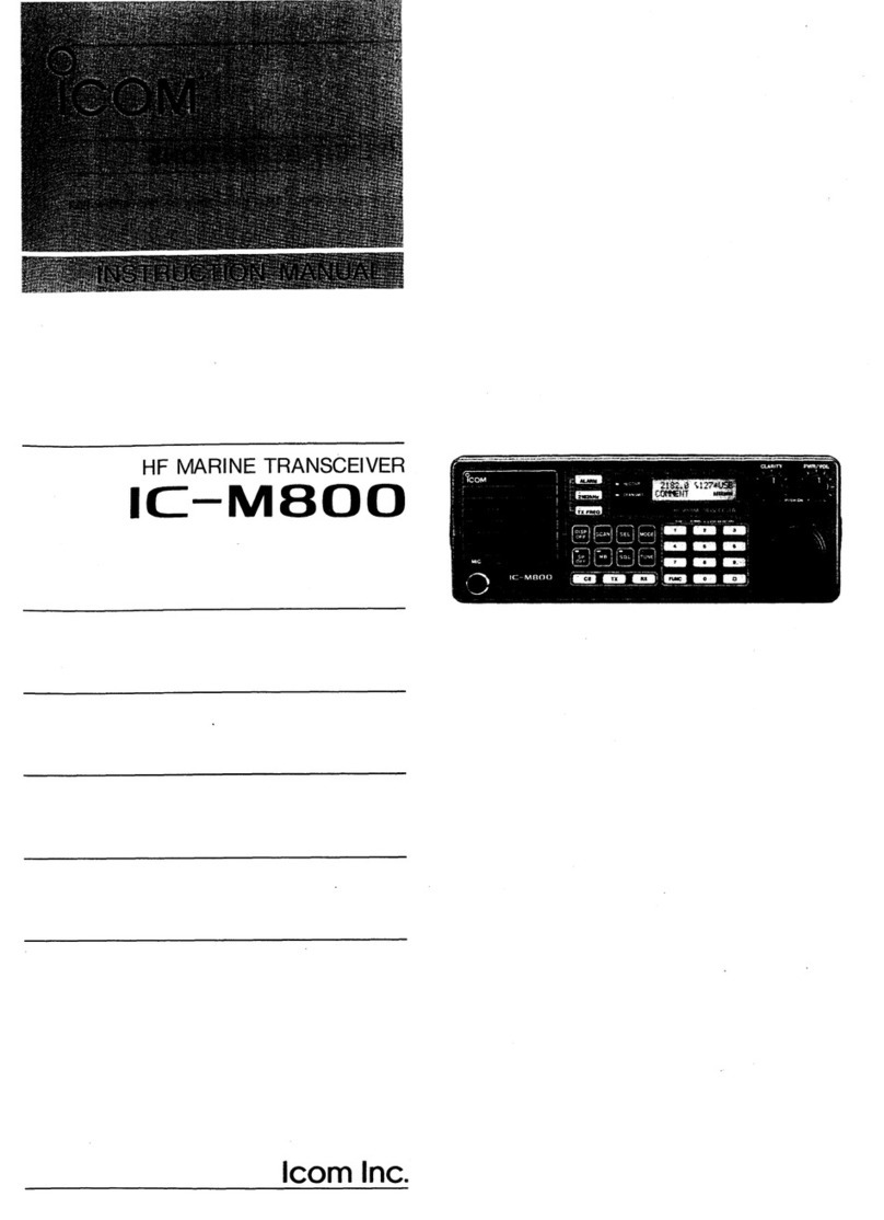
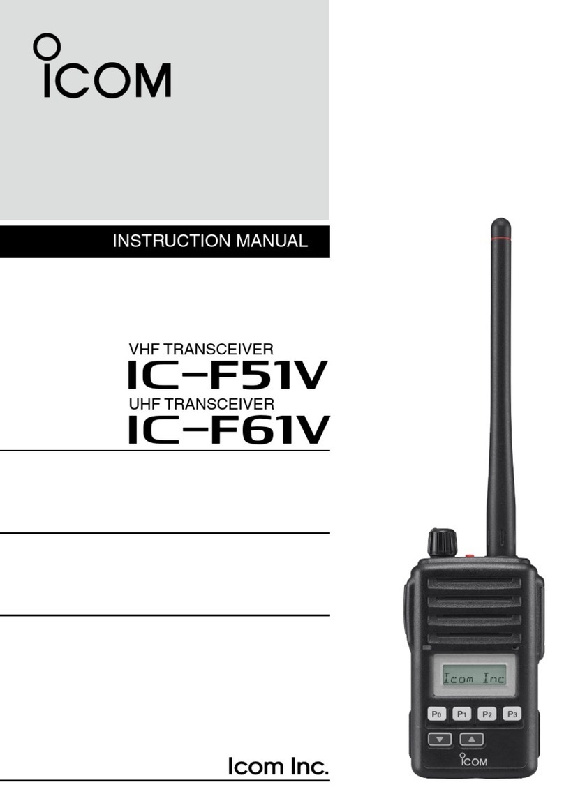
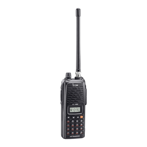
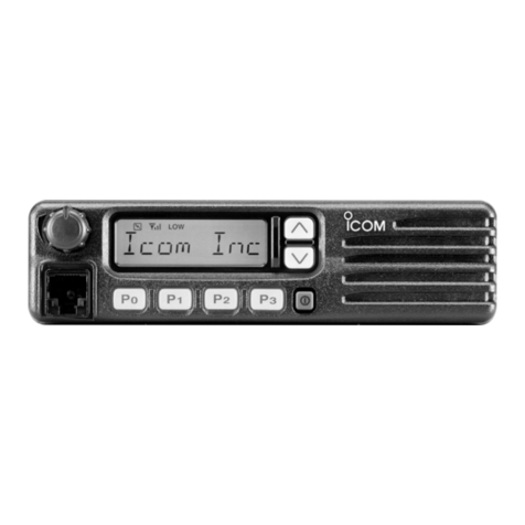
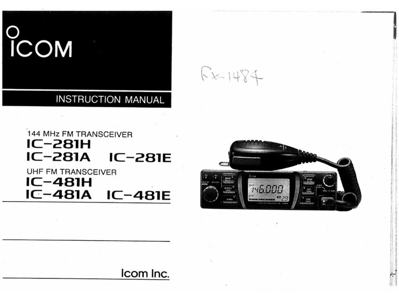
Icom IC-F4011 User manual

S-14605XZ-C1
May. 2009
UHF TRANSCEIVERS

This service manual describes the latest service information
for the IC-F4011/IC-F4013 UHF TRANSCEIVERS at the time
of publication.
NEVER connect the transceiver to an AC outlet or to a DC
power supply that uses more than specifed. This will ruin
the transceiver.
DO NOT expose the transceiver to rain, snow or any liquids.
DO NOT reverse the polarities of the power supply when
connecting the transceiver.
DO NOT apply an RF signal of more than 20 dBm (100 mW) to
the antenna connector. This could damage the transceiver’s
front-end.
To upgrade quality, any electrical or mechanical parts and
internal circuits are subject to change without notice or
obligation.
Be sure to include the following four points when ordering
replacement parts:
1. 10-digit Icom parts numbers
2. Component name
3. Equipment model name and unit name
4. Quantity required
<ORDER EXAMPLE>
1110003491 S.IC TA31136FNG IC-F4011 MAIN UNIT 5 pieces
8820001210 Screw 2438 screw IC-F4013 Top cover 10 pieces
Addresses are provided on the inside back cover for your
convenience.
Icom, Icom Inc. and ICOM logo are registered trademarks of Icom Incorporated (Japan) in the United States, the United
Kingdom, Germany, France, Spain, Russia and/or other countries.
ORDERING PARTS
1. Make sure that the problem is internal before
disassembling the transceiver.
2. DO NOT open the transceiver until the transceiver is
disconnected from its power source.
3. DO NOT force any of the variable components. Turn
them slowly and smoothly.
4. DO NOT short any circuits or electronic parts. An
insulated tuning tool MUST be used for all adjustments.
5. DO NOT keep power ON for a long time when the
transceiver is defective.
6. DO NOT transmit power into a Standard Signal
Generator or a Sweep Generator.
7. ALWAYS connect a 50 dB to 60 dB attenuator between
the transceiver and a Deviation Meter or Spectrum
Analyzer when using such test equipment.
8. READ the instructions of test equipment throughly
before connecting a test equipment to the transceiver.
REPAIR NOTES
INTRODUCTION
CAUTION
(IC-F4011)
MODEL VERSION FREQ.
(MHz)
CHANNEL
SPACING CHANNELS
F4011 USA-06 400–470
12.5/25.0 kHz 16CH
USA-07 450–512
F4013
CSA-01 400–470
CSA-02 450–512
CSA-03 400–470
CSA-04 450–512

TABLE OF CONTENTS
SECTION 1 SPECIFICATIONS
SECTION 2 INSIDE VIEWS
SECTION 3 DISASSEMBLY INSTRUCTION
SECTION 4 CIRCUIT DESCRIPITON
4-1 RECEIVER CIRCUITS. . . . . . . . . . . . . . . . . . . . . . . . . . . . . . . . . . . . . . . . . . . . . . . . . . . . . . . . 4-1
4-2 TRANSMITTER CIRCUITS . . . . . . . . . . . . . . . . . . . . . . . . . . . . . . . . . . . . . . . . . . . . . . . . . . . . 4-2
4-3 PLL CIRCUITS. . . . . . . . . . . . . . . . . . . . . . . . . . . . . . . . . . . . . . . . . . . . . . . . . . . . . . . . . . . . . . 4-4
4-4 OTHER CIRCUITS . . . . . . . . . . . . . . . . . . . . . . . . . . . . . . . . . . . . . . . . . . . . . . . . . . . . . . . . . . 4-5
4-5 POWER SUPPLY CIRCUITS. . . . . . . . . . . . . . . . . . . . . . . . . . . . . . . . . . . . . . . . . . . . . . . . . . . 4-5
4-6 PORT ALLOCATIONS . . . . . . . . . . . . . . . . . . . . . . . . . . . . . . . . . . . . . . . . . . . . . . . . . . . . . . . . 4-5
SECTION 5 ADJUSTMENT PROCEDURES
5-1 PREPARATION . . . . . . . . . . . . . . . . . . . . . . . . . . . . . . . . . . . . . . . . . . . . . . . . . . . . . . . . . . . . . 5-1
5-2 FREQUENCY ADJUSTMENTS. . . . . . . . . . . . . . . . . . . . . . . . . . . . . . . . . . . . . . . . . . . . . . . . . 5-6
5-3 TRANSMIT ADJUSTMENTS . . . . . . . . . . . . . . . . . . . . . . . . . . . . . . . . . . . . . . . . . . . . . . . . . . . 5-8
5-4 RECEIVERY ADJUSTMENTS. . . . . . . . . . . . . . . . . . . . . . . . . . . . . . . . . . . . . . . . . . . . . . . . . . 5-10
SECTION 6 PARTS LIST
SECTION 7 MECHANICAL PARTS
SECTION 8 BOARD LAYOUTS
SECTION 9 BLOCK DIAGRAM
SECTION 10 VOLTAGE DIAGRAM

1 - 1
SECTION 1
.
SPECIFICATIONS
PGENERAL
• Frequency coverage : 400–470 MHz [USA-06], [CSA-01], [CSA-03]
450–512 MHz [USA-07], [CSA-02], [CSA-04]
• Type of emission : 16K0F3E (25.0 kHz) for Wide
: 11K0F3E (12.5 kHz) for Narrow
• Channel spacing : 12.5/25.0 kHz
• Number of conventional channels : 16 ch
• Antenna impedance : 50 Ω
• Operating temperature range : –30˚C to +60˚C (–22˚F to +140˚F)
• Power supply requirement : Specified Icom's battery pack only (7.2 V DC nominal; negative ground)
• Current drain (at 7.2 V DC ; approx.) :
RECEIVING TRANSMITTING
Stand-by Max. audio
High (at 4 W) Low (at 1 W)
75 mA 300 mA 1.6 A 0.8 A
• Dimensions (projections not included) : 53.0 (W)×120.0 (H)×38.0 (D) mm; 23⁄32(W)×423⁄32(H)×11⁄2(D) in
• Weight (Including BP-231) : Approx. 260 g (93⁄16 oz)
PTRANSMITTER
• Output power (at 7.2 V DC) : 4 W (Hi)/2 W (L2)/1 W (L1)
• Modulation : Variable reactance frequency modulation
• Maximum permissible deviation : ±5.0 kHz (Wide), ±2.5 kHz (Narrow)
• Frequency error : ±2.5 ppm
• Spurious emissions : 70 dB (min.)
• Adjacent channel power : 70 dB min. (75dB typ.) for Wide
60 dB min. (68dB typ.) for Narrow
• Audio harmonic distortion : 3% typ. (at 1 kHz, 40% deviation)
• FM Hum and Noise
(without CCITT filter)
: 40 dB min. (46 dB typ.) for Wide
34 dB min. (40 dB typ.) for Narrow
• Limiting charact of modulator : 60–100% of maximum deviation
• Microphone impedance : 2.2 kΩ
PRECEIVER
• Receive system : Double conversion superheterodyne system
• Intermediate frequencies : 1st IF: 46.35 MHz, 2nd IF: 450 kHz
• Sensitivity : 0.25 µV (–119 dBm) typ. at 12 dB SINAD
• Adjacent channel selectivity : 70 dB min. (75 dB typ.) for Wide
60 dB min. (65 dB typ.) for Narrow
• Spurious response : 70 dB min.
• Intermodulation rejection ratio : 70 dB min. (74 dB typ.)
• Hum and Noise (without CCITT filter) : 40 dB min. (45 dB typ.) for Wide
34 dB min. (40 dB typ.) for Narrow
• Audio output power : 0.5 W typ. (at 5% distortion with an 8 Ωload)
• Squelch sensitivity (at threshold) : 0.25 µV typ.
• Output impedance (audio) : 8 Ω
Specifications are measured in accordance with TIA-603.
All stated specifications are subject to change without notice or obligation.

2 - 1
SECTION 2
.
INSIDE VIEWS
+5 Regulator
(IC9: NJM2870F05)
AF amplifier
(IC12: TA7368F)
D/A converter
(IC8: M62363FP)
R5 Regulator
(Q22: 2SA1577)
CPU
(IC13: HD6433687A91
F
S5 Regulator
Q23: 2SB1132
Q24: XP6501
Q25: UNR9113G0L
Crystal filter
(FI1: FL-335)
FM IF IC
(IC1: TA31136FNG)
IF amplifier
(Q4: 2SC4215)
EEPROM
(IC15: BR24L16FV)
Power amplifier
(Q7: RD07MVS2)
T5 Regulator
(Q21: 2SA1577)
PLL IC
(IC4: MB15A02PFV1)
Pre-drive
(Q5: 2SC3356)
APC amplifier
(IC2: TC75S51F)
VCO circuit
TOP VIEW BOTTOM VIEW
• MAIN UNIT
Drive amplifier
(Q8: RD01MUS2)

3 - 1
SECTION 3
.
DISASSEMBLY INSTRUCTION
1. REMOVING THE CHASSIS UNIT
qUnscrew 1 nut A, and remove 2 knobs B, C.
wUnscrew 2 screws D.
eTake off the chassis unit in the direction of the arrow.
rUnplug the connector Efrom the chassis unit.
2. REMOVING THE MAIN UNIT
qUnscrew 2 nuts F, and remove the top plate G.
wUnsolder 5 points H, and remove the shield cover.
eUnscrew 2 screws I, and remove the side plate J.
rUnscrew 7 screws K.
tUnsolder 4 points L, and take off the main unit in the
direction of the arrow.
Chassis unit D
A
B
C
E
Main unit
I
K
KL
K
FG
Chassis unit
L
H
H
J
Shield cover

4 - 1
SECTION 4
.
CIRCUIT DESCRIPTION
4-1 RECEIVER CIRCUITS
4-1-1 ANTENNA SWITCHING CIRCUIT
The antenna switching circuit functions as a low-pass filter
while receiving and a resonator circuit while transmitting.
This circuit does not allow transmit signals to enter the
receiver circuits.
Received signals enter the antenna connector (CHASSIS;
J1) and pass through the low-pass filters (ANT UNIT; L601,
C601) and (MAIN UNIT; L1, L2, L45, C1–C6, C175). The
filtered signals are passed through the 1⁄4λtype antenna
switching circuit (D2, D5, L6) and then applied to the RF cir-
cuit.
4-1-2 RF CIRCUIT
The RF circuit amplifies signals within the range of frequen-
cy coverage and filters out-of-band signals.
The signals from the antenna switching circuit pass through
the bandpass filter (D3, D4, D7, D8). The filtered signals are
amplified at the RF amplifier (Q2) and then passed through
the another bandpass filter (D9, D10, C38–C40, C44, C45)
to suppress unwanted signals. The filtered signals are
applied to the 1st mixer circuit.
D3, D4, D7–D10 employ varactor diodes, that are con-
trolled by the CPU via the D/A converter (IC8), to track
the bandpass filter. These varactor diodes tune the center
frequency of an RF passband for wide bandwidth receiving
and good image response rejection.
4-1-3 1ST MIXER AND 1ST IF CIRCUITS
The 1st mixer circuit converts the received signal into fixed
frequency of the 1st IF signal with the PLL output frequency.
By changing the PLL frequency, only the desired frequency
passes through a crystal filter at the next stage of the 1st
mixer.
The RF signals from the bandpass filter are mixed with the
1st LO signals, where come from the RX VCO circuit via the
BPF (L38, C49, C304, C305), at the 1st mixer circuit (Q3)
to produce a 46.35 MHz 1st IF signal. The 1st IF signal is
passed through a monolithic filter (FI1) in order to obtain
selection capability and to pass only the desired signal.
The filtered signal is applied to the 2nd IF circuit after being
amplified at the 1st IF amplifier (Q4).
4-1-4 2ND IF AND DEMODULATOR CIRCUITS
The 2nd mixer circuit converts the 1st IF signal into a 2nd
IF signal. The double-conversion superheterodyne system
(which converts receive signals twice) improves the image
rejection ratio and obtains stable receiver gain.
The 1st IF signal from the IF amplifier (Q4) is applied to
the 2nd mixer section of the FM IF IC (IC1, pin 16), and
is mixed with the 2nd LO signal to be converted into a
450 kHz 2nd IF signal.
The FM IF IC (IC1) contains the 2nd mixer, 2nd local oscil-
lator, limiter amplifier, quadrature detector, active filter and
noise amplifier circuits. A 2nd LO signal (45.9 MHz) is pro-
duced at the PLL circuit by tripling it’s reference frequency
(15.3 MHz).
The 2nd IF signal from the 2nd mixer (IC1, pin 3) passes
through the ceramic filter (FI2) to remove unwanted hetero-
dyned frequencies. It is then amplified at the limiter amplifier
section (IC1, pin 5) and applied to the quadrature detector
section (IC1, pins 10, 11) to demodulate the 2nd IF signal
into AF signals.
The demodulated AF signals are output from pin 9 (IC1) as
“DET” signal, and are then applied to the AF circuit.
Mixer
16
Limiter
AMP
2nd IF filter
450 kHz X2
15.3 MHz
45.9 MHz
IC1 TA31136FN
12 1st IF signal from the IF amplifier (Q4)
"RSSI" signal to the CPU (IC13, pin 63)
11109
87 5
AF signal "DET"
to the AF circuit
"SQLC" signal from the
D/A converter IC
(IC8, pin 2)
To D/A converter IC
(IC8, pin 1)
R5V
X1
2
Active
filter
Noise
detector
FM
detector
13
"NOIS" signal to the CPU (IC13, pin 53)
RSSI
Noise
AMP
Noise
comparator
×3
Q19
FI2
3
• 2ND IF AND DEMODULATOR CIRCUITS

4 - 2
4-1-5 AF AMPLIFIER CIRCUIT
The AF amplifier circuit amplifies the demodulated AF sig-
nals to drive a speaker.
The AF signals from the FM IF IC (IC1, pin 9) pass through
the high-pass filter (IC6, pins 3 and 1) to suppress unwant-
ed harmonic components. The signals pass through the
RX mute switch (Q34) which is controlled by “RMUT” sig-
nal from the CPU (IC13, pin 56), and are then applied to
another high-pass filter (IC6, pins 13 and 14). The filtered
signals pass through the low-pass filter (IC6, pins 6 and 7)
via the analog switch (IC10, pins 1 and 2). The signals are
applied to the analog switch (IC10, pin 10) again, and are
then applied to the AF power amplifier (IC12, pin 4) via the
AF volume (R226). The amplified AF signals are output from
pin 10, and are then applied to the internal speaker which is
connected with J1 via the [SP] jack.
4-1-6 RECEIVE MUTE CIRCUITS
• NOISE SQUELCH
A squelch circuit cuts out AF signals when no RF signals
are received. By detecting noise components in the AF sig-
nals, the squelch circuit switches the AF mute switch.
Some noise components in the AF signals from the FM IF
IC (IC1, pin 9) are applied to the D/A converter (IC8, pin 1)
as “DET” signal, and are then output from pin 2. The signals
are applied to the active filter section in the FM IF IC (IC1,
pin 8). The active filter section filters and amplifies noise
components. The amplified signals are converted into the
pulse-type signals at the noise detector section and output
from pin 13 as “NOIS” signal.
The “NOIS” signal from the FM IF IC is applied to the CPU
(IC13, pin 53). Then the CPU analyzes the noise condition
and outputs the AF mute control signal from the CPU (IC13)
as “RMUT” signal from pin 56. The signal is applied to the
RX mute switch (Q34) to control the AF signal muting.
• CTCSS AND DTCS
The tone squelch circuit detects tone signals and opens the
squelch only when receiving a signal containing a matched
subaudible tone (CTCSS or DTCS). When the tone squelch
is in use, and a signal with a mismatched or no subaudible
tone is received, the tone squelch circuit mutes the AF sig-
nals even when noise squelch is open.
A portion of the “DET” signals from the FM IF IC (IC1,
pin 9) passes through the low-pass filter (IC7, pins 5 and 7)
to remove AF (voice) signals, and are then applied to the
amplifier (IC7, pin 3). The amplified signals are applied to
the CTCSS or DTCS decoder inside of the CPU (IC13,
pin 60) as the “CDEC” signal. The CPU outputs AF mute
control signal from pin 56, and is then applied to the RX
mute switch (Q34) and analog switch (IC10, pins 12 and 13)
to control AF signals muting as “RMUT” signal.
4-2 TRANSMITTER CIRCUITS
4-2-1 MICROPHONE AMPLIFIER CIRCUIT
The microphone amplifier circuit amplifies audio signals
within +6 dB/octave pre-emphasis characteristics from the
microphone to a level needed for the modulation circuit.
The AF signals from the microphone are passed through
the microphone mute switch (Q35), and are then applied
to the amplifier (IC6, pins 9 and 8) via the high-pass filter
(IC6, pins 13 and 14). The amplified signals are applied to
the analog switch (IC10, pin 4), and outputs from pin 3. The
signals pass through the low-pass filter (IC6, pins 6 and 7),
then applied to the analog switch (IC10, pin 9) again and
output from pin 8.
The signals are applied to the D/A converter (IC8, pin 4).
The converted signals output from pin 3, and applied to the
modulation circuit (D18) as “MOD” signal.
Analog SW
(IC10)
"DET" AF signal
from FM IF IC (IC1, pin 9)
8
AF
volume
AF
AMP
MIC
MUTE
IC12
Q35
Speaker
R226
IC8 D18
RX
MUTE
Q34
LPF
IC6 B
HPF
IC6 D
HPF
IC6 A
Microphone
IC6 C
AMP
1
4
3
2
9
10
D/A converter FM mod.
"CTCSS/DTCS" signal from
D/A conveter IC (IC8, pin 10)
"TONE" signal from CPU (IC13) via low-pass
filters (IC5 A / IC5 B pin 7)
to TX VCO circuit
(Q13, D16, D17)
11
• ANALOG SWITCHING CIRCUITS

4 - 3
4-2-2 MODULATION CIRCUIT
The modulation circuit modulates the VCO oscillating signal
(RF signal) using the audio signals from the microphone.
The AF signals from the D/A converter (IC8, pin 3) change
the reactance of varactor diode (D18) to modulate the oscil-
lated signal at the TX VCO circuit (Q13, D17, D18, D21).
The modulated VCO signal is amplified at the buffer amplifi-
ers (Q10, Q12) and then applied to the drive amplifier circuit
via the T/R switch (D14, D15).
The CTCSS/DTCS signals (“CENC0”, “CENC1”, ”CENC2”)
from the CPU (IC13, pins 23–25) pass through the low-pass
filter (IC5, pins 12 and 14) via 3 registers (R191–R193) to
change its wave form. Then the signals are applied to the
D/A converter (IC8, pin 9). The output signals from the D/
A converter (IC8, pin 10) pass through the low-pass filter
(IC6, pins 6 and 7) to be mixed with “MOD” signal, and then
applied to the D/A converter again (IC8, pin 4).
4-2-3 DRIVE/POWER AMPLIFIER CIRCUITS
The drive/power amplifier circuits amplify the VCO oscillat-
ing signal to a transmit power level.
The modulated RF signal from the TX VCO circuit passes
through the T/R switch (D14, D15) and is amplified at the
YGR (Q9), pre-drive (Q5), drive (Q8), and power (Q7)
amplifiers to obtain 4 W of RF power (at 7.2 V DC).
The amplified signal passes through the low-pass filter (L1,
L2, L45, C1–C5, C175, C176), antenna switch (D2) and
power detector (D1, D30), then applied to the antenna con-
nector (CHASSIS unit; J1).
4-2-4 APC CIRCUITS
The bias current of the drive (Q8) and power (Q7) amplifiers
are controlled by the APC circuit.
The APC circuit (IC2, D1, D30) protects drive and power
amplifiers from the reflected signal, and selects output
power of HIGH, LOW2 or LOW1.
The power detector (D1, D30) detects transmit output power
and converts it into DC voltage. The DC voltage is at a mini-
mum level when the antenna impedance is matched to 50 Ω,
and increased when mismatched.
The detected voltage is applied to the differential amplifier
(IC2, pin 3), and the “T2” signal from the D/A converter (IC8,
pin 23), controlled by the CPU (IC13), is applied to pin 1 for
reference. When antenna impedance is mismatched, the
detected voltage exceeds the power setting voltage. Then
the output voltage of the differential amplifier (IC2, pin 4)
controls the input current of the drive (Q8), and power (Q7)
amplifiers to reduce the output power.
Power
AMP
Differential
AMP
Driver
AMP
+
–
VCC
to ANT unit
T2
TMUT
RF signal
from Buffer AMP
T5V
D1
YGR
AMP
ANT
SW LPF
LPF
Q8
IC2
Q9 Q7
D2
• APC CIRCUITS
4 - 4
4-3 PLL CIRCUITS
4-3-1 PLL CIRCUIT
A PLL circuit provides stable oscillation for the transmit fre-
quency and the receive 1st LO frequency. The PLL output
compares the phase of the divided VCO frequency to the
reference frequency. The PLL output frequency is controlled
by the divided ratio (N-data) of a programmable divider.
The PLL circuit contains the TX/RX VCO circuits (TX:
Q13, D17, D21; RX: Q14, D16, D21). The oscillated sig-
nal is amplified at the buffer amplifiers (Q11, Q12) and
then applied to the PLL IC (IC4, pin 8) after being passed
through the low-pass filter (L32, C206, C208).
The phase detected signal is output from pins 15 and 16,
and passes through the loop filter (C130, C138, C146,
C147, R95–R97), then applied to the TX and RX VCO cir-
cuits as a lock voltage.
The PLL IC contains a prescaler, programmable counter,
programmable divider and phase detector, etc. The entered
signal is divided at the prescaler and programmable counter
section by the N-data ratio from the CPU. The divided signal
is detected on phase at the phase detector using the refer-
ence frequency.
If the oscillated signal drifts, its phase changes from that of
the reference frequency, causing a lock voltage change to
compensate for the drift in the oscillated frequency.
4-3-2 VCO CIRCUITS
The VCO circuit contains a separate RX VCO (Q14, D16,
D22) and TX VCO (Q13, D17, D18, D21). The oscillated
signal is amplified at the buffer amplifiers (Q10, Q12) and
is then applied to the T/R switch (D14 for TX, D15 for RX).
Then the receive 1st LO (RX) signal is applied to the 1st
mixer circuit (Q3) and the transmit (TX) signal to the pre-
YGR amplifier (Q9).
A portion of the signal from the buffer amplifier (Q12) is fed
back to the PLL IC (IC4, pin 8) via the buffer amplifier (Q11)
and low-pass filter (L32, C206, C208) as the comparison
signal.
Shift register
Prescaler
Phase
detector
Loop
filter
Programmable
counter
Programmable
divider
X2
15.3 MHz
2
Buffer
Q12
Buffer
Q18
Buffer
Q10
Buffer
Q11
14
15
16
SCK
SO
PLST
to transmitter circuit
to 1st mixer circuit
D14
D15
1
15
16
8
Q13, D16, D17, D21
TX VCO
Q14, D19, D20, D22
RX VCO
IC4 MB15A02
3
45.9 MHz 2nd LO
signal to the FM IF IC
(IC1, pin 2) Tripler
Q19
"LVIN" signal to the CPU
(IC13, pin 64)
LPF
Charge
Pump
Q39, Q40
• PLL CIRCUITS
4 - 5
LINE
VCC
+5V
S5V
R5V
T5V
DESCRIPTION
The voltage from the attached battery pack.
Common 5 V converted from the VCC line at
the +5 regulator circuit (IC9). The output voltage
is supplied to the D/A converter (IC8), analog
SW (IC10) and so on.
Common 5 V converted from the VCC line at
the S5 regulator circuit (Q23–Q25). The output
voltage is supplied to the ripple filter (Q17), PLL
IC (IC4), etc.
Receive 5 V converted from the S5V line at the
R5 regulator circuit (Q22). The output voltage
is supplied to the tripler (Q19), FM IF IC (IC1),
IF amplifier (Q4), VCO switch (Q15, Q16), 1st
mixer (Q3), etc.
Transmit 5 V converted from the S5V line at the
T5 regulator circuit (Q21). The output voltage is
supplied to the YGR (Q9), pre-drive (Q5), APC
amplifier (IC2), etc..
4-5 POWER SUPPLY CIRCUIT
VOLTAGE LINE
4-4 OTHER CIRCUITS
LED CONTROL CIRCUITS
The LED control circuit is composed of the LED driver (Q32)
and LED (DS1).
The CPU outputs “RLED” and “TLED” signals from the pins
42 and 43. The signals are applied to the LED driver (Q32,
pins 2 and 5).
BAL
T2
T1
LVA
REF
Outputs the modulation balance level
control signal. The signal is applied to
the buffer amplifier (IC7, pin 3).
•
Outputs the bandpass filter tuning
signal during receive. The output
signal is applied to the bandpass
filters (D9, D10).
• Outputs the TX power control signal
during transmit. The output signal is
applied to the APC amplifier (IC2,
pin 1).
Outputs the bandpass filter tuning
signal. The output signal is applied to
the bandpass filters (D4, D8).
Outputs the PLL lock voltage control
signal. The output signal is applied to
the buffer amplifier (IC7, pin 3).
Outputs the reference oscillator
correcting voltage. The voltage is applied
to the buffer amplifier (IC7, pin 5).
Pin Port Description
number name
4-6 PORT ALLOCATION
4-6-1 D/A CONVERTER IC (IC8)
11
23
22
14
15
CONDITION COLOR
RECEIVING (2/5-TONE CODE) ORANGE (Lighting)
LOW BATTERY
(Nearly exhausted) RED (Blinks Slowly)
LOW BATTERY
(Almost exhausted) RED (Blinks Fast)
CLONING ORANGE (Blinking)
RECEIVING/SQUELCH OPEN GREEN (Lighting)
TRANSMITTING RED (Lighting)

4 - 6
Pin
number
Port
name Description
1 TEMP
Input port for the transceiver’s
internal temperature detecting
signal.
2BATV
Input port for the detect signal for
connecting battery pack’s voltage.
7 RES Input port for power reset signal.
13 SENC0 Output single tone encoder
signal.
14 SENC1
16 DUSE Outputs DTSC LPF control
signal.
18 AFON Outputs AF power amplifier
control signal.
19 SENC2 Output single tone encoder
signal.
20 SENC3
21 CBI0 Input ports for ritary selectoir.
22 CBI1
23 CENC0
Output CTCSS/DTCS signals.
24 CENC1
25 CENC2
26 CBI2 Input ports for rotary selector.
27 CBI3
28 SCK
Outputs serial clock signal to the
PLL IC (IC4, pin 9), D/A convertor
(IC8, pin 7), etc.
29 SO
Outputs serial data to the PLL IC
(IC4, pin 8) and D/A convertor
(IC8, pin 8).
30 BEEP Outputs beep audio signals.
31 ESDA I/O port for data signals from/to
the EEPROM (IC15, pin 5).
32 ESCL Outputs clock signal to the
EEPROM (IC15, pin 6).
33 UNLK Input port for unlock signal from
PLL IC IC4, pin 9).
34 PLST Outputs strobe signals to the PLL
IC (IC4, pin 11).
36 NWC Output/input port for wide/narrow
control signal.
37 DAST
• Outputs strobe signals to the D/
A convertor (IC8, pin 6).
• Input port for the connecting
battery type detect signal.
38 S5C Outputs power save control
signal.
39 T5C
Outputs T5 regurator control
signal.
Low: While transmitting
40 R5C
Outputs R5 regurator control
signal.
Low: While receivinging
Pin
number
Port
name Description
42 RLED Outputs receiving LED control signal.
43 TLED Outputs transmitting LED control
signal.
47 PTT
Input port for the PTT switch detection
signal.
Low : While the PTT switch is pushed.
48 SI Serial Bus inputport.
49 CLI Input port for the cloning data signal.
50 CLO Outputs the cloning data signal.
53 NOIS Input port for the noise signal from the
FM IF IC (IC1, pin 13).
55 CCS Outputs chip select signal.
56 TMUT Outputs transmit mute signal.
57 RMUT Input port for AF mute signal from the
RX circuit.
58 MMUT Outputs MIC mute signal.
59 REMO Inputs key signal from remote mic.
60 CDEC Input port for CTCSS/DTCS signal
from the amplifier (IC5, pin 8).
61 SDEC Input port for single tone decode
signal from the LPF (IC5, pin 8).
62 KEY Inputs key input signal.
63 RSSI Input port for the S-meter signal from
the FM IF IC (IC1, pin 12).
64 LVIN Input port for the PLL lock voltage
.
4-6-2 CPU (IC13)

5 - 1
SECTION 5
.
ADJUSTMENT PROCEDURE
¤ SYSTEM REQUIREMENTS
• Microsoft®Windows®98/SE/ME/2000/XP
• RS-232C/USB port
¤ BEFORE STARTING SOFTWARE ADJUSTMENT
Clone adjustment frequencies, TX power, CTCSS frequency, DTCS code and IF bandwidth into the transceiver using the
CS-F3011/F3013 CLONING SOFTWARE before starting adjustment.
CAUTION!: BACK UP the originally programmed memory data in the transceiver before programming the adjustment
frequencies. When program the adjustment frequencies into the transceiver, the transceiver’s memory data will be
overwritten and lose original memory data at the same time.
5-1 PREPARATION
¤ REQUIRED EQUIPMENTS
EQUIPMENT SPECIFICATION EQUIPMENT SPECIFICATION
Adjustment
software "CS-F3010 ADJ" (Revision 1.0 or later) JIG cable
(see the page 5-3)
Modified OPC-478U/UC (USB type) or
OPC-478 (RS-232 type)
Audio generator Frequency range : 300–3000 Hz
Output level : 1–500 mV Attenuator Power attenuation : 30 dB
Capacity : More than 10 W
RF power meter
(terminated type)
Measuring range :
1–10 W
Frequency range : 100–600 MHz
Impedance : 50
Ω
SWR : Less than 1.2 : 1
Standard signal
generator (SSG)
Frequency range : 0.1–600 MHz
Output level : 0.1 µV to 32 mV
(–127 to –17 dBm)
Frequency counter
Frequency range : 0.1–600 MHz
Frequency accuracy
: ±1 ppm or better
Input level : Less than 1 mW
AC millivoltmeter Measuring range : 10 mV to 10 V
Oscilloscope Frequency range : DC–20 MHz
Measuring range : 0.01–20 V
Modulation
analyzer
Frequency range : 30–600 MHz
Measuring range : 0 to ±10 kHz External speaker Input impedance : 8 Ω
Capacity : More than 1 W
¤ ADJUSTMENT CHANNEL SETTING
qUsing the CS-F3011/F3013 CLONING SOFTWARE, create the cloning data for adjustments as shown below.
wClone the data file into the transceiver.
• For [Low band] • For [High band]
Microsoft, Windows and Windows Vista are registered trademarks
of Microsoft Corporation in the United States and/or other coun-
tries.

5 - 2
2-conductor 2.5 (d) mm plug
(MIC)
(GND)
33 k
3-conductor 3.5(d) mm plug
(CLONE)
OPC-478/U/UC
(GND)
(SP)
[JIG cable1]
[JIG cable2]
+−
AC
MILLIVOLTMETER
(10 mV to 10 V)
AUDIO GENERATOR
(300–3000 Hz/1–500 mV)
+−
PTT
+
4.7 µF
EXT. SPEAKER
(1 W/8 Ω)
+
−
SETTING;
Frequency : 1 kHz
Level : 150 mVrms
Waveform : Sine wave
• CONNECTION
• JIG CABLE
FM
deviation meter
SINAD meter
Speaker (8 Ω)
to the antenna connector
Attenuator
30 dB
RF power meter
0.1–10 W/50 Ω
Frequency
counter
Standard signal generator
0.1 µV to 32 mV
(–127 dBm to –17 dBm)
DO NOT transmit while
an SSG is connected to
the antenna connector.
To [SP]
To [MIC]
JIG cables
To [SP] connector
PC
to USB port
to USB port
to RS-232C port
OPC-478
(RS-232C type)
OPC-478U
(USB type)
OPC-478UC
(USB type)

5 - 3
(PC SCREEN EXAMPLE
PSTARTING SOFTWARE ADJUSTMENT
(1) Connect the transceiver and PC with OPC-478/U/UC and JIG CABLE (see the previous page).
(2) Turn the transceiver power ON.
(3) Boot up Windows, and click the program group 'CS-F3010 ADJ’ in the ‘Programs’ folder of the [Start] menu, then CS-F3010
ADJ’s window appears.
(4) Click ‘Connect’ on the CS-F3010’s window, then IC-F4011/F4013’s up-to-date condition appears as below.
(5) Set or modify adjustment value as specified in the following guidances.
NOTE: The above screen is an example.
Each transceiver has its own specific values for each setting.

5 - 4
5-2 FREQUENCY ADJUSTMENT
1) Select an adjustment item using cursor or [↑] / [↓] of the PC’s keyboard.
2) Set or modify the adjustment value as specified using [←] / [→] of the PC’s keyboard, then push [ENTER].
ADJUSTMENT ADJUSTMENT CONDITION OPERATION ADJUSTMENT
ITEM VALUE
PLL LOCK
VOLTAGE
1–• Connect an RF power meter to the
antenna. ––
RX 2 • Channel : CH.1
• Receiving
• Adjust the [RX LVA] using [←] / [→]
on the PC’s keyboard until the “LVIN”
in the “ADJUSTMENT WINDOW”
shows the specified value, then push
[ENTER].
or
• Set the [RX LVA] to "51", then push
[ENTER].
[RX LVA]
1.0 V
(at the "LVIN"
item)
or
"51"
(at the [RX/TX
LVA])
TX 3 • Channel : CH.1
• Transmitting
• Adjust the [TX LVA] using [←] / [→]
on the PC’s keyboard until the “LVIN”
in the “ADJUSTMENT WINDOW”
shows the specified value, then push
[ENTER].
or
• Set the [TX LVA] to "51", then push
[ENTER].
[TX LVA]
LOCK
VOLTAGE
VERIFICATION
1
–
• Connect an RF power meter to the
antenna. ––
RX 2 • Channel : CH.2
• Receiving
• Verify the lock voltage displayed at
the "LVIN" in the "ADJUSTMENT
WINDOW" (see the previous page).
[LVIN]
3.3–4.5 V
(Verify)
TX 3 • Channel : CH.2
• Transmitting
3.3–4.5 V
[Low band]
3.0–4.2 V
[High band]
(Verify)
REFERENCE
FREQUENCY
1–• Loosely couple a frequency counter
to the antenna connector. –
–
2 • Channel : CH.2
• Transmitting
1) Adjust the frequency using [←] / [→]
on the PC’s keyboard.
2) Push [ENTER] to store the adjust
value.
[REF]
470.0000 MHz
[Low band]
512.0000 MHz
[High band]

5 - 5
5-3 TRANSMIT ADJUSTMENT
1) Select an adjustment item using cursor or [↑] / [↓] of the PC’s keyboard.
2) Set or modify the adjustment value as specified using [←] / [→] of the PC’s keyboard, then push [ENTER].
ADJUSTMENT ADJUSTMENT CONDITION OPERATION
ADJUSTMENT
ITEM VALUE
TRANSMIT
OUTPUT
POWER
1
–
• Connect an RF power meter to the
antenna connector. ––
Hi power 2 • Channel : CH.3
• Transmitting
1) Adjust the transmit output power
using [←] / [→] on the PC’s key-
board.
2) Push [ENTER] to store the adjust
value.
[Power (Hi)] 4.0 W
L2 power 3 • Channel : CH.4
• Transmitting [Power (L2)]
2.0 W
L1 power 4 • Channel : CH.5
• Transmitting [Power (L1)]
1.0 W
DEVIATION
-Preparation-
1•Connect a modulation analyzer
to the antenna connector
through an Attenuator.
• Set the modulation analyzer as;
HPF : OFF
LPF : 20 kHz
De-emphasis : OFF
Detector : (P-P)/2
––
2•Connect an audio generator to
the MIC line through the JIG
cable.
• Set the audio generator as;
Modulation : 1 kHz
Level : 150 mV rms
Wave form : Sine wave
––
-Adjustment-
NARROW
3 • Channel : CH.6
• Transmitting
1) Adjust the deviation using [←] / [→]
on the PC’s keyboard.
2) Push [ENTER] to store the adjust
value.
[MOD N] ±2.05–2.15
kHz
MODULATION
BALANCE
-Preparation-
1•Connect a modulation analyzer
to the antenna connector
through an attenuator.
• Set the modulation analyzer as;
HPF : OFF
LPF : 20 kHz
De-emphasis : OFF
Detector : (P-P)/2
––
• Connect an oscilloscope to
the Detect terminal of the
modulation analyzer.
–––
-Adjustment-
NARROW
2 • Channel : CH.9
• No audio signals are applied.
• Transmitting
1) Adjust the waveform using [←] / [→]
on the PC’s keyboard.
2) Push [ENTER] to store the adjust
value.
[BAL N]
Square
waveform
WIDE 4 • Channel :
CH.10
• No audio signals are applied.
• Transmitting [BAL Ratio]
CTCSS/DTCS
DEVIATION
-Preparation-
1•Connect a modulation analyzer
to the antenna connector
through an attenuator.
• Set the modulation analyzer as;
HPF : OFF
LPF : 20 kHz
De-emphasis : OFF
Detector : (P-P)/2
––
-Adjustment- 2 • Channel :
CH.11
• No audio signals are applied.
• Transmitting
1) Adjust the deviation using [←] / [→]
on the PC’s keyboard.
2) Push [ENTER] to store the adjust
value.
[CTCSS/DTCS] ±0.66–0.70
kHz

5 - 6
5-4 RECEIVE ADJUSTMENT
1) Select an adjustment item using cursor or [↑] / [↓] of the PC’s keyboard.
2) Set or modify the adjustment value as specified using [←] / [→] of the PC’s keyboard, then push [ENTER].
ADJUSTMENT ADJUSTMENT CONDITION OPERATION ADJUSTMENT
ITEM VALUE
RECEIVE
SENSITIVITY
-Preparation-
1•Connect an SSG to the ant-
enna connector.
• Set the SSG as;
Frequency : 400.1000 MHz
[Low band]
450.1000 MHz
[High band]
Level :
+20 dBµ (–87 dBm)†
Modulation : 1 kHz
Deviation : 3.5 kHz
––
-Adjustment- 2 • Channel :
CH.12
• Receiving
1) Select the [BPF (T1)] item, then
push [ENTER].
2) Select the [BPF (T2)] item, then
push [ENTER].
[BPF (T1)]
[BPF (T2)]
(Automatic
adjustment)
CONVINIENT: [BPF (T1)] and [BPF (T2)] can be adjusted at the same time as below.
2 • Channel :
CH.12
• Receiving
• Select the [BPF ALL] item, then
push [ENTER]. [BPF ALL]
(Automatic
adjustment)
SQUELCH
-Preparation-
1•Connect an SSG to the ant-
enna connector.
• Set the SSG as;
Frequency : 400.1000 MHz
[Low band]
450.1000 MHz
[High band]
Level :
–14 dBµ (–121 dBm)†
Modulation : 1 kHz
Deviation : 3.5 kHz
––
-Adjustment- 2 • Channel :
CH.12
• Receiving
1) Once close the squelch by
increasing the value of [SQL] item,
then decrease the value to open
the squelch.
2) Push [ENTER] to store the value.
[SQL]
(Automatic
adjustment)
†; The output level of the standard signal generator (SSG) is indicated as the SSG’s open circuit.

6 - 1
SECTION 6
.
PARTS LIST
L601 6200013010 S.COI 0.30-0.9-5TL 10.3N <COMO> B 7.2/12.5
C601 4030017600 S.CER ECJ0EC1H080C B 5.8/15.3
REF PARTS DESCRIPTION M. H/V
NO. NO.
LOCATION
[ANT UNIT]
M.=Mounted side (T: Mounted on the Top side, B: Mounted on the Bottom side)
S.=Surface mount
REF PARTS DESCRIPTION M. H/V
NO. NO.
LOCATION
[CONNECT UNIT]
C501 4030017460 S.CER ECJ0EB1E102K T 8.3/5.3
C502 4030016930 S.CER ECJ0EB1A104K T 9.3/5.3
J501 6910016390 CON IMSA-9230B-1-02Z145-PT1

6 - 2
REF PARTS DESCRIPTION M. H/V
NO. NO.
LOCATION
[MAIN UNIT]
IC1 1110003201 S.IC TA31136FNG(EL) B 51.8/19
IC2 1130008561 S.IC TC75S51F(TE85L,F) T 68.9/21
IC4 1140005991 S.IC MB15A02PFV1-G-BND-ERE1 T 38.3/35.7
IC5 1110005340 S.IC NJM12902V-TE1-#ZZZB T 28.6/7.1
IC6 1110005320 S.IC NJM13403V-TE1-#ZZZB T 15.9/34.6
IC8 1190000350 S.IC M62363FP-650C T 40.3/15.2
IC9 1110005350 S.IC NJM2870F05-TE1-#FZZB B 84.2/14.2
IC10 1130011770 S.IC CD4066BPWR T 22.9/34.6
IC12 1110001811 S.IC TA7368FG(5,ER) T 89.3/13.2
IC13 1140012721 S.IC HD6433687C73FPV(FX-2775A-1) T 12.5/14.3
IC14 1110006260 S.IC BD5242G-TR T 6.6/5.9
IC15 1130011540 S.IC BR24L16FV-WE2 B 16/11.6
Q1 1560000841 S.FET 2SK1829(TE85R,F) T 75/39.6
Q2 1580000731 S.FET 3SK293(TE85L,F) B 76.8/37.9
Q3 1580000800 S.FET 3SK324UG-TL-E B 66.3/37.9
Q4 1530002601 S.TRA 2SC4215-O(TE85R,F) B 51.4/23.1
Q5 1530000371 S.TRA 2SC3356-T1B S (R25) T 74.3/33.5
Q6 1590003231 S.TRA UNR9113G0L T 72.5/19.1
Q7 1560001232 S.FET RD07MVS2-T112 T 82.6/27
Q8 1560001241 S.FET RD01MUS1-T113 T 76.1/27.5
Q9 1530003311 S.TRA 2SC5107-O(TE85R,F) T 67/30.3
Q10 1530003311 S.TRA 2SC5107-O(TE85R,F) T 59.4/36.3
Q11 1530003311 S.TRA 2SC5107-O(TE85R,F) B 56.3/37
Q12 1530003311 S.TRA 2SC5107-O(TE85R,F) T 59/31.5
Q13 1530002920 S.TRA 2SC4226-T1 R25 T 54.9/30.7
Q14 1530002920 S.TRA 2SC4226-T1 R25 T 54.2/37.1
Q15 1590001400 S.TRA XP1214(TX) B 56.5/32.6
Q16 1590003291 S.TRA UNR9213G0L B 59.1/32.6
Q17 1530002851 S.TRA 2SC4116-BL(TE85R,F) T 55.5/44.1
Q18 1560000541 S.FET 2SK880-Y(T5RICOM,F) B 51.8/41.2
Q19 1530002851 S.TRA 2SC4116-BL(TE85R,F) T 43.3/29.9
Q21 1510000920 S.TRA 2SA1577 T106 Q T 71.9/16.4
Q22 1510000920 S.TRA 2SA1577 T106 Q T 24.9/25.9
Q23 1520000460 S.TRA 2SB1132 T100 R T 81/15.2
Q24 1590001190 S.TRA XP6501-(TX).AB T 76.2/14.4
Q25 1590003231 S.TRA UNR9113G0L B 77/14.6
Q27 1590003291 S.TRA UNR9213G0L T 24.8/16.7
Q28 1590003431 S.TRA UNR911HG0L B 63.1/10.6
Q29 1590003271 S.TRA UNR9210G0L B 35.7/9.2
Q30 1510001080 S.TRA 2SA2048 TLR T 91.9/8.6
Q31 1590001190 S.TRA XP6501-(TX).AB T 91.4/5.2
Q32 1590003020 S.TRA XP4216-(TX) T 16.5/23.1
Q34 1560001360 S.FET 2SK3019 TL T 10.7/30.1
Q35 1560001360 S.FET 2SK3019 TL T 8.4/26.6
D1 1750001080 S.DIO RB886G T2R B 90.7/40.1
D2 1750000581 S.DIO 1SV307(TPH3,F) B 91.5/31.1
D3 1750000711 S.VAR HVC350BTRF-E B 86/35
D5 1790001261 S.DIO MA2S077G0L B 86.5/39.3
D6 1790001241 S.DIO MA2S7280GL B 84.5/39.9
D7 1750000711 S.VAR HVC350BTRF-E B 81.6/35
D9 1750000711 S.VAR HVC350BTRF-E B 73.6/35.9
D10 1750000711 S.VAR HVC350BTRF-E B 72.2/35.9
D14 1790001261 S.DIO MA2S077G0L T 65.8/35.5
D15 1790001261 S.DIO MA2S077G0L T 65.8/36.9
D16 1750000711 S.VAR HVC350BTRF-E T 52.1/38.9
D17 1750000711 S.VAR HVC350BTRF-E T 49.4/28.3
D18 1720000570 S.VAR MA368(TX) B 49.6/26.9
D21 1750000711 S.VAR HVC350BTRF-E T 50.5/33.7
D22 1750000711 S.VAR HVC350BTRF-E T 50.5/35.2
D24 1790001251 S.DIO MA2S1110GL T 41.5/39.2
D25 1790001251 S.DIO MA2S1110GL T 70.5/40.4
D26 1790001790 S.DIO RB876W TL B 35.7/7.1
D27 1750000520 S.DIO DAN222TL B 21.3/6
D28 1790001261 S.DIO MA2S077G0L B 8.5/11.2
D29 1750000940 S.DIO ISS400 TE61 B 23.1/4
D30 1750001080 S.DIO RB886G T2R T 88.5/36.2
FI1 2030000150 S.MON DSF753SB 46.350 MHz(FL-335) B 62.8/27.1
FI2 2020002410 CER LTM450FW <JJE>
FI3 2040001440 S.LC NFE31PT152Z1E9L
(NFM60R20T152) B 81.2/17.8
X1 6070000300 S.DIS JTBM450CX24 <JJE> T 54.4/20
X2 6050012050 S.XTA CR-794 TTS14VSB-A6 15.3 MHz T 36.9/28.9
X3 6050011720 S.XTA CR-764 SMD-49TB 19.6608 MHz
<KDS> B 12/5.9
L1 6200012490 S.COI 0.30-0.9-6TR 13.6N <COMO> B 94.7/36.4
L2 6200013010 S.COI 0.30-0.9-5TL 10.3N <COMO> B 94.8/31.9
L3 6200012610 S.COI 0.40-0.9-2TL 2.8N <COMO> B 92.9/26.3
L4 6200012610 S.COI 0.40-0.9-2TL 2.8N <COMO> B 89.9/20.6
L5 6200010850 S.COI LQW18AN22NG00D
(LQW1608A22NG00) [USA-06] B 89.3/36.4
6200009070 S.COI LQW18AN18NG00D
(LQW1608A18NG00) [USA-07]
6200010850 S.COI LQW18AN22NG00D
(LQW1608A22NG00) [CSA-01]
6200009070 S.COI LQW18AN18NG00D
(LQW1608A18NG00) [CSA-02]
6200010850 S.COI LQW18AN22NG00D
(LQW1608A22NG00) [CSA-03]
6200009070 S.COI LQW18AN18NG00D
(LQW1608A18NG00) [CSA-04]
M.=Mounted side (T: Mounted on the Top side, B: Mounted on the Bottom side)
S.=Surface mount
REF PARTS DESCRIPTION M. H/V
NO. NO.
LOCATION
[MAIN UNIT]
L7 6200007700 S.COI LQW2BHN22NJ03L [USA-06] B 84.3/34.5
6200007690 S.COI LQW2BHN18NJ03L [USA-07]
6200007700 S.COI LQW2BHN22NJ03L [CSA-01]
6200007690 S.COI LQW2BHN18NJ03L [CSA-02]
6200007700 S.COI LQW2BHN22NJ03L [CSA-03]
6200007690 S.COI LQW2BHN18NJ03L [CSA-04]
L8 6200007700 S.COI LQW2BHN22NJ03L [USA-06] B 79.9/34.6
6200007690 S.COI LQW2BHN18NJ03L [USA-07]
6200007700 S.COI LQW2BHN22NJ03L [CSA-01]
6200007690 S.COI LQW2BHN18NJ03L [CSA-02]
6200007700 S.COI LQW2BHN22NJ03L [CSA-03]
6200007690 S.COI LQW2BHN18NJ03L [CSA-04]
L9 6200007680 S.COI LQW2BHN12NJ03L [USA-06] B 75.9/35.2
6200007670 S.COI LQW2BHN10NJ03L [USA-07]
6200007680 S.COI LQW2BHN12NJ03L [CSA-01]
6200007670 S.COI LQW2BHN10NJ03L [CSA-02]
6200007680 S.COI LQW2BHN12NJ03L [CSA-03]
6200007670 S.COI LQW2BHN10NJ03L [CSA-04]
L11 6200007230 S.COI LQW2BHN15NJ03L [USA-06] B 70.6/37.8
6200007680 S.COI LQW2BHN12NJ03L [USA-07]
6200007230 S.COI LQW2BHN15NJ03L [CSA-01]
6200007680 S.COI LQW2BHN12NJ03L [CSA-02]
6200007230 S.COI LQW2BHN15NJ03L [CSA-03]
6200007680 S.COI LQW2BHN12NJ03L [CSA-04]
L12 6200011001 S.COI ELJRF 56NJFB B 64.2/39
L13 6200004770 S.COI ELJNC R56J-F [USA-06] B 66.8/33.7
6200007850 S.COI ELJNC R82K-F [USA-07]
6200004770 S.COI ELJNC R56J-F [CSA-01]
6200007850 S.COI ELJNC R82K-F [CSA-02]
6200004770 S.COI ELJNC R56J-F [CSA-03]
6200007850 S.COI ELJNC R82K-F [CSA-04]
L15 6200002851 S.COI NLV25T-R82J T 94.2/32.4
L17 6200012980 S.COI 0.40-1.4-5TR 18.3N <COMO> B 81.2/20.9
L19 6200005671 S.COI ELJRE 12NGFA [USA-06] T 76/35.5
6200005661 S.COI ELJRE 10NGFA [USA-07]
6200005671 S.COI ELJRE 12NGFA [CSA-01]
6200005661 S.COI ELJRE 10NGFA [CSA-02]
6200005671 S.COI ELJRE 12NGFA [CSA-03]
6200005661 S.COI ELJRE 10NGFA [CSA-04]
L20 6200005691 S.COI ELJRE 18NGFA [USA-06] T 68.8/33.1
6200005681 S.COI ELJRE 15NGFA [USA-07]
6200005691 S.COI ELJRE 18NGFA [CSA-01]
6200005681 S.COI ELJRE 15NGFA [CSA-02]
6200005691 S.COI ELJRE 18NGFA [CSA-03]
6200005681 S.COI ELJRE 15NGFA [CSA-04]
L21 6200007881 S.COI ELJRF 33NJFB T 59.2/38.6
L22 6200007901 S.COI ELJRF 22NJFB T 59.5/33.3
L23 6200002851 S.COI NLV25T-R82J T 55.2/28.1
L25 6200013630 S.COI 0.30-0.9-3TR 5.8N 5PER
<COMO> T 49.5/29.9
L26 6200013580 S.COI 0.30-0.9-4TR 5PER <COMO> T 49/37.9
L27 6200004951 S.COI NLV25T-1R8J B 52.8/29
L28 6200004951 S.COI NLV25T-1R8J B 51.7/37
L29 6200004660 S.COI MLF1608A 1R8K-T T 43.9/36.4
L30 6200007881 S.COI ELJRF 33NJFB B 85.1/38.7
L32 6200007911 S.COI ELJRF 18NJFB B 55.8/40.8
L33 6200004480 S.COI MLF1608D R82K-T T 43.4/25.9
L35 6200003540 S.COI MLF1608D R22K-T T 41.7/31.8
L38 6200005711 S.COI ELJRE 27NGFA B 65.6/40.7
L40 6200002851 S.COI NLV25T-R82J T 53.6/34.6
L41 6200007881 S.COI ELJRF 33NJFB B 58.4/38.1
L42 6200004951 S.COI NLV25T-1R8J B 49.4/34
L43 6200004951 S.COI NLV25T-1R8J B 49.4/31.1
L45 6200012490 S.COI 0.30-0.9-6TR 13.6N <COMO> B 95.2/39.6
R1 7030003490 S.RES ERJ3GEYJ 272 V (2.7K) B 92.3/37.6
R2 7030005120 S.RES ERJ2GEJ 102 X (1K) B 91.1/38.2
R3 7030004970 S.RES ERJ2GEJ 470 X (47) [USA-06] T 66.7/22.7
7030005570 S.RES ERJ2GEJ 820 X (82) [USA-07]
7030004970 S.RES ERJ2GEJ 470 X (47) [CSA-01]
7030005570 S.RES ERJ2GEJ 820 X (82) [CSA-02]
7030004970 S.RES ERJ2GEJ 470 X (47) [CSA-03]
7030005570 S.RES ERJ2GEJ 820 X (82) [CSA-04]
R4 7030005050 S.RES ERJ2GEJ 103 X (10K) T 75.8/20.8
R5 7030005050 S.RES ERJ2GEJ 103 X (10K) [USA-06] T 73.3/21.1
7030005220 S.RES ERJ2GEJ 223 X (22K) [USA-07]
7030005050 S.RES ERJ2GEJ 103 X (10K) [CSA-01]
7030005220 S.RES ERJ2GEJ 223 X (22K) [CSA-02]
7030005050 S.RES ERJ2GEJ 103 X (10K) [CSA-03]
7030005220 S.RES ERJ2GEJ 223 X (22K) [CSA-04]
R6 7030005090 S.RES ERJ2GEJ 104 X (100K) T 66.7/18.2
R7 7030005310 S.RES ERJ2GEJ 124 X (120K) T 68/17.7
R8 7030005170 S.RES ERJ2GEJ 474 X (470K) [USA-06] T 71.3/21.1
7030005100 S.RES ERJ2GEJ 154 X (150K) [USA-07]
7030005170 S.RES ERJ2GEJ 474 X (470K) [CSA-01]
7030005100 S.RES ERJ2GEJ 154 X (150K) [CSA-02]
7030005170 S.RES ERJ2GEJ 474 X (470K) [CSA-03]
7030005100 S.RES ERJ2GEJ 154 X (150K) [CSA-04]
R9 7030008280 S.RES ERJ2GEJ 271 X (270) T 71.3/22.4
R10 7030005120 S.RES ERJ2GEJ 102 X (1K) T 68.4/24
R11 7030005090 S.RES ERJ2GEJ 104 X (100K) T 84/35.8
R12 7030005530 S.RES ERJ2GEJ 100 X (10) T 77.5/37.5
R13 7030005090 S.RES ERJ2GEJ 104 X (100K) T 82.3/35.8
R14 7030005050 S.RES ERJ2GEJ 103 X (10K) T 84/36.7
R15 7030005240 S.RES ERJ2GEJ 473 X (47K) B 79.1/38.4
R16 7030004980 S.RES ERJ2GEJ 101 X (100) B 74.8/39.9
R17 7030004970 S.RES ERJ2GEJ 470 X (47) B 74/33.3
R18 7030005050 S.RES ERJ2GEJ 103 X (10K) T 78.8/36.7
R19 7030005080 S.RES ERJ2GEJ 823 X (82K) T 78.8/38.7
This manual suits for next models
1
Table of contents
Other Icom Transceiver manuals