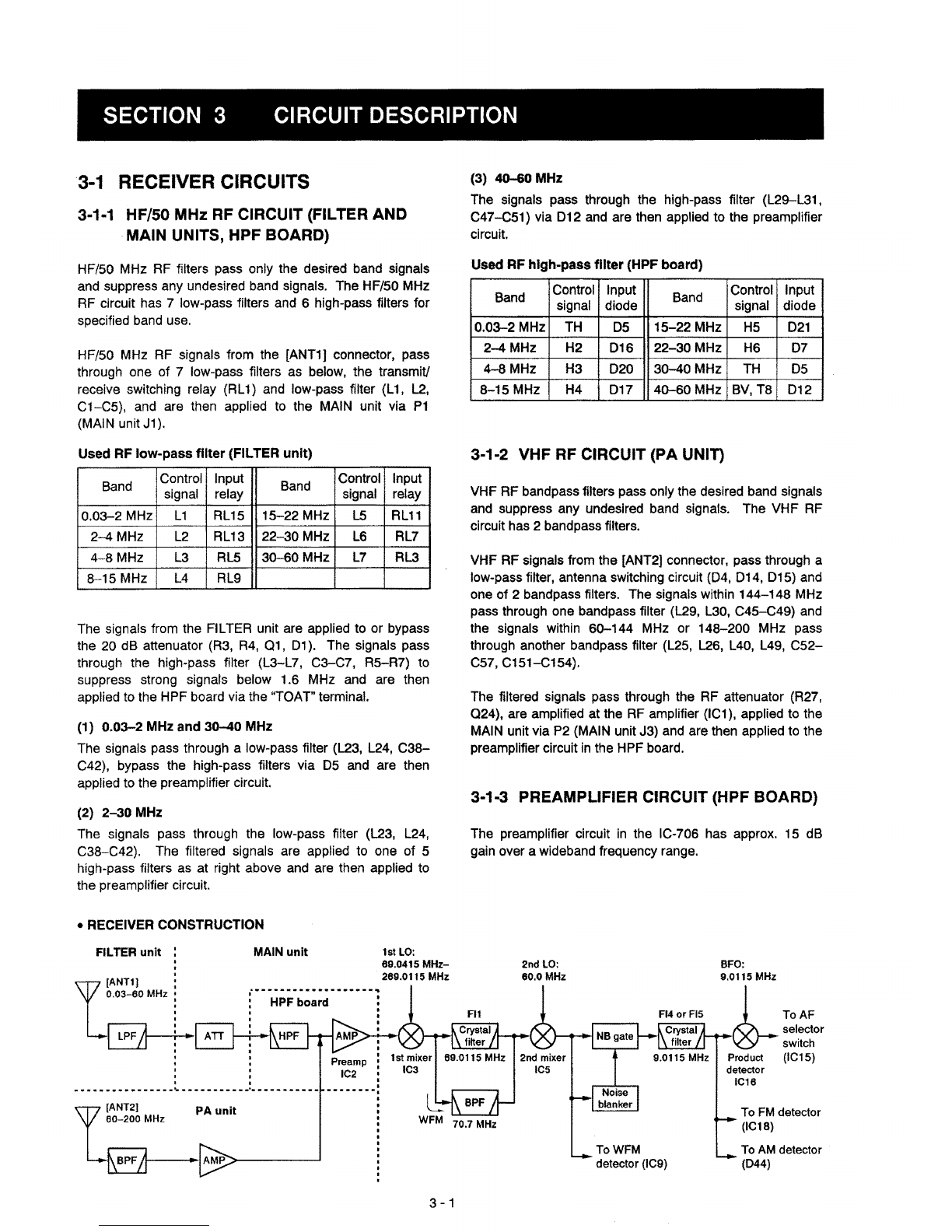
3-1-5 1
st
IF CIRCUIT (MAIN UNIT)
Mode Frequency
SSB,
FM
69.0115 MHz
CW,
RTTY 69.0106 MHz
AM
69.0100 MHz
WFM 70.7000 MHz
The 1st IF signals from IC4 are converted to 9MHz or 10.7
MHz 2nd IF signals at the 2nd mixer (IC5).
The
2nd
mixer circuit mixes the amplified 1st IF signals and
2nd
LO
signal (60.00 MHz)
to
convert the 1
st
IF
to
a
2nd
IF.
Mode Frequency
SSB,
FM
9.0115 MHz
CW,RTIV
9.0106 MHz
AM
9.0100 MHz
WFM 10.7000 MHz
When the preamplifier is turned ON, the signals from the RF
circuit are applied to the preamplifier
(ICl)
via 025. Ampli-
fied or bypassed signals enter the
MAIN
unit via the "AMPI"
terminal and are applied to the 1st mixer circuit (IC3).
3-1-4
1st
MIXER CIRCUIT (MAIN UNIT)
The 1
st
mixer circuit mixes the receive signals with the 1
st
LO
signal to convert the receive signal frequencies to a69
or 70.7 MHz 1st IF.
The signals from the preamplifier circuit, or signals which
bypass the preamplifier, are applied to alow-pass filter and
then to the 1st mixer (IC3).
The 1st
LO
signal 1
st
IFfrequency
(69.0415-269.0115 MHz)
enters the MAIN unit from
the PLL unit via J4. The
LO
signal is amplified at
04,
filtered
by
alow-pass
filter, and then, applied to
the 1st mixer.
The 1st IF circuit filters and amplifies the 1st IF signals. The
1st IF signals are applied to an MCF (Monolithic Crystal
Filter;
Fll
a,
Fll
b)
to suppress out-of-band signals.
While
in
non-WFM modes, the 69 MHz 1st IF signals pass
through the pair of MCF's
(Fll)
and are applied to the IF
amplifier (IC4). While
in
WFM mode, the 70.7 MHz 1st IF
signal pass through abandpass filter (L1
04-L
108,
C358-
C361) and are applied to the IF amplifier (IC4).
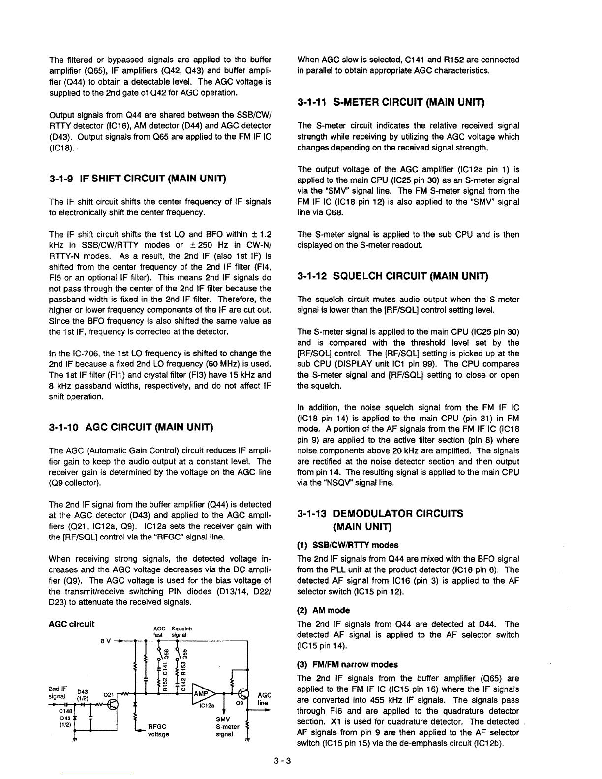
The AGC voltage is supplied to the transmit/receive switch-
ing circuit (013, 014) and 013/014 function as
PIN
attenu-
ators for AGC operation.
The amplified signals are then applied to the 2nd mixer
(IC5).
3-1-6 2nd MIXER CIRCUIT (MAIN UNIT)
The 2nd IF signals are 2nd IFfrequency
applied to Fl3 to suppress
undesired signals such as
the 2nd
LO
signal, and are
then applied to the noise
blanker gate (020, 021).
3-2
While in
FM
(normal) mode, the IFsignals pass through the
low-pass filter (L52, C82-C84) bypassing
Fll
and the noise
blanker gate and are then applied to the 2nd IF circuit.
While
in
WFM mode, the IF signals pass through the low-
pass filter (L52, C82-C84), IF amplifier (05), ceramic
filter:
(FI2) and IF amplifier (052). The signals are then applied
to the
FM
IF
IC
(IC9) for demodulation into AF signals.
3-1-7 NOISE BLANKER CIRCUIT (MAIN UNIT)
The noise blanker circuit detects pulse type noise, and turns
OFF the signal line when noise appears.
The 2nd IF signals from FI3 are applied to the noise blanker
gate (020, 021). Aportion of the signals from FI3 are
amplified at the noise amplifiers (010,
012,
amplifier sec-
tion of IC9), then detected at the noise detector (039) to
convert the noise components to
OC
voltages.
The signals are then applied to the noise blanker switch
(013, 014). At the moment the detected voltage exceeds
the
013's
threshold level,
014
outputs ablanking signal to
close the noise blanker gate (020, 021) by applying
reverse-biased voltage.
The detected voltage from
039
is also applied to the noise
blanker AGC circuit (011,
016)
and is then fed back to the
amplifier (IC9) as abias voltage. The noise AGC circuit
prevents closure
of
the noise blanker gate for long periods
by
non-pulse-type noise. The time constant of the noise
blanker AGC circuit is determined by R143
and
C459.
The signals from the noise blanker gate are then applied to
the 2nd IF circuit.
3-1-8 2nd IF CIRCUIT (MAIN UNIT)
The 2nd IFcircuit amplifies and filters the 2nd IF signals.
Both the signals passed through and bypassing the noise
blanker gate (020, 021) are amplified at IC6 via
022
and
applied to a2nd IF filter as shown
in
the following table.
2nd IFfilters
Mode Used filter Control signal
SSB med.,
CW
med., FL-30 (FI4) 2F23
RTTY med.,
AM
nar.
AM
FL-116 (Fl5) 2F60
FM,
FM
nar. Bypassed 2NTH
SSB nar. Optional FL-223 2FOP
CW
nar., RTTY nar. Optional FL-l00, 2FOP
FL-l
01,
FL-223
SSB
Wide,
CW wide, Optional
FL-l03
2FOP
RTTYwide
The AGC voltage is supplied to the transmit/receive switch-
ing
circuit (022, 023) and 022/023 function
as
PIN
attenu-
ators for AGC operation.