Icom IC-F1000 series User manual

S-15106XZ-C1
August 2014
VHF TRANSCEIVERS

This service manual describes the latest technical informa-
tion for the IC-F1000 series VHF TRANSCEIVERS, at the time of
publication.
NEVER connect the transceiver to an AC outlet or to a DC
power supply that uses more than the specified voltage. This
will ruin the transceiver.
DO NOT expose the transceiver to rain, snow or liquids.
DO NOT reverse the polarities of the power supply when con-
necting the transceiver.
DO NOT apply an RF signal of more than 20 dBm (100 mW) to
the antenna connector. This could damage the transceiver’s
front-end.
To upgrade quality, any electrical or mechanical parts
and internal circuits are subject to change without notice
or obligation.
MODEL VERSION VERSION
NUMBER
FREQUENCY
RANGE (MHz) KEY TYPE
IC-F1000
USA-01 [#01]
136–174
–
EUR-01 [#02]
UK-01 [#03]
EXP-01 [#04]
IC-F1000S
USA-01 [#05]
4-key
EUR-01 [#06]
UK-01 [#07]
EXP-01 [#08]
IC-F1000T
USA-01 [#09]
10-key
EUR-01 [#10]
UK-01 [#11]
EXP-01 [#12]
IC-F1000T-T THA-01 [#13]
Be sure to include the following four points when ordering
replacement parts:
1. 10-digit Icom part number
2. Component name
3. Equipment model name and unit name
4. Quantity required
<ORDER EXAMPLE>
1110003491 S.IC TA31136FNG IC-F1000 MAIN UNIT 5 pieces
8820001210 Screw 2438 screw IC-F1000S Top cover 10 pieces
Addresses are provided on the inside back cover for your
convenience.
ORDERING PARTS
1. Make sure that the problem is internal before dis-assem-
bling the transceiver.
2. DO NOT open the transceiver until the transceiver is dis-
connected from its power source.
3. DO NOT force any of the variable components. Turn them
slowly and smoothly.
4. DO NOT short any circuits or electronic parts. An insulated
tuning tool MUST be used for all adjustments.
5. DO NOT keep power ON for a long time when the trans-
ceiver is defective.
6. DO NOT transmit power into a Standard Signal Generator
or a Sweep Generator, otherwise the RF power may dam-
age them.
7. ALWAYS connect a 30 dB to 40 dB attenuator between the
transceiver and a Deviation Meter or Spectrum Analyzer,
when using such test equipment.
8. READ the instructions of the test equipment thoroughly
before connecting it to the transceiver.
REPAIR NOTES
INTRODUCTION
CAUTION
(IC-F1000T)
Icom, Icom Inc. and the Icom logo are registered trademarks of Icom Incorporated (Japan) in Japan, the United States, the
United Kingdom, Germany, France, Spain, Russia and/or other countries.

TABLE OF CONTENTS
SECTION 1 SPECIFICATIONS
SECTION 2 INSIDE VIEWS
SECTION 3 DISASSEMBLY INSTRUCTION
SECTION 4 CIRCUIT DESCRIPITON
4-1 RECEIVER CIRCUITS...................................................................................... 4-1
4-2 TRANSMITTER CIRCUITS............................................................................... 4-2
4-3 FREQUENCY SYNTHESIZER CIRCUITS ....................................................... 4-4
4-4 VOLTAGE BLOCK DIAGRAM ........................................................................... 4-4
4-5 PORT ALLOCATIONS ...................................................................................... 4-5
SECTION 5 ADJUSTMENT PROCEDURES
5-1 PREPARATION ................................................................................................. 5-1
5-2 FREQUENCY ADJUSTMENT .......................................................................... 5-3
5-3 TRANSMIT ADJUSTMENT............................................................................... 5-4
5-4 RECEIVE ADJUSTMENT ................................................................................. 5-5
SECTION 6 PARTS LIST
SECTION 7 MECHANICAL PARTS
SECTION 8 BOARD LAYOUTS
SECTION 9 BLOCK DIAGRAM
SECTION 10 VOLTAGE DIAGRAM

1-1
SECTION 1
.
SPECIFICATIONS
M GENERAL
• Frequency range: 136–174 MHz
• Number of conventional channels: 16 channels
• Type of emission:
(Occupied band-width)
[EXP], [THA] Wide: 16K0F3E (25.0 kHz)
Narrow: 11K0F3E (12.5 kHz)
[USA] Narrow: 11K0F3E (12.5 kHz)
[EUR], [UK] Wide: 16K0F3E (25.0 kHz)
Middle: 14K0F3E (20.0 kHz)
Narrow: 8K50F3E (12.5 kHz)
• Antenna impedance: 50 (Nominal)
• Operating temperature range: –30˚C to +60˚C: –22˚F to +140˚F (Except [EUR], [UK].)
–25˚C to +55˚C (For [EUR], [UK].)
• Power supply voltage: Specified Icom's battery packs only (7.5 V DC: negative ground)
• Current drain (Approximately): Receiving 77 mA (stand-by)
330 mA (maximum audio, internal speaker)
Transmitting 1.3 A (at 5 W)
• Dimensions:
(Projections not included)
With BP-278
52.2(W)×111.5(H)×22.3(D) mm: 2.1(W) × 4.4(H) × 0.9(D) in
ches
With BP-279
52.2(W)×111.5(H)×24.5(D) mm: 2.1(W) × 4.4(H) × 1(D) inches
• Weight (Approximately): With BP-278 230 g: 8.1 oz.
With BP-279 240 g: 8.5 oz.
• Intermediate frequencies: 1st 46.35 MHz
2nd 450 kHz
• Output impedance (Speaker): 8
• Input impedance (Microphone): 2.2 k
M TRANSMITTER
• Output power: 5 W
• Modulation: Variable reactance frequency modulation
• Maximum frequency deviation: Wide ±5.0 kHz
Middle ±4.0 kHz
Narrow ±2.5 kHz
• Frequency stability: ±2.5 ppm
• Spurious emissions: 70 dB minimum (Except [EUR], [UK].)
0.25 µW (1 GHz), 1.0 µW (1 GHz) (For [EUR], [UK].)
• Adjacent channel power: Wide 70 dB minimum, 74 dB typical
Middle 70 dB minimum, 72 dB typical
Narrow 60 dB minimum, 70 dB typical
• Audio harmonic distortion: Wide 1.0% typical at AF 1 kHz 40% deviation
Middle 1.0% typical at AF 1 kHz 40% deviation
Narrow 1.5% typical at AF 1 kHz 40% deviation
• FM hum and Noise:
(Except [EUR], [UK])
(Without CCITT FILTER)
Wide 40 dB minimum, 46 dB typical
Narrow 34 dB minimum, 40 dB typical
• Residual modulation
([EUR], [UK])
:
(With CCITT FILTER)
Wide 45 dB minimum, 50 dB typical
Middle 43 dB minimum, 47 dB typical
Narrow 40 dB minimum, 44 dB typical
• Limitting charact of modulator: 60–100% of maximum deviation

1-2
M RECEIVER
• Sensitivity: 0.25 µV typical at 12 dB SINAD (Except [EUR], [UK].)
–4.0 dBµV emf typical at 20 dB SINAD (For [UK], [EUR].)
• Intermodulation: 70 dB minimum, 74 dB typical (Except [EUR], [UK].)
65 dB minimum, 68 dB typical (For [UK], [EUR].)
• Spurious response: 70 dB minimum
• Audio output power: 0.8 W typical at 5% distortion into the 12 internal speaker.
0.4 W typical at 5% distortion into an 8 external speaker.
• Hum and noise (Except [EUR], [UK]):
(Without CCITT Filter)
Wide 40 dB minimum, 51 dB typical
Narrow 34 dB minimum, 45 dB typical
• Hum and noise (For [EUR], [UK]):
(With CCITT Filter)
Wide 45 dB minimum, 52 dB typical
Middle 43 dB minimum, 49 dB typical
Narrow 40 dB minimum, 46 dB typical
• Adjacent channel selectivity: Wide 70 dB minimum, 76 dB typical
Middle 70 dB minimum, 72 dB typical
Narrow 40 dB minimum, 53 dB typical
• Squelch sensitivity: 0.25 µV typical (Except [EUR], [UK].)
–4 dBµV emf typical (For [UK], [EUR].)
Specifications are measured in accordance with TIA-603 or EN 300 086.
All stated specifications are subject to change without notice or obligation.

2-1
SECTION 2
.
INSIDE VIEWS
• MAIN UNIT
(TOP VIEW)
AF POWER AMP
CONTROLLER (Q9)
VOX AMP
(IC3)
BASEBAND IC
(IC4)
BASEBAND IC CLOCK
(X1)
APC AMP
(IC17)
MIC GAIN CONTROLLER
(IC2)
5 V REGULATOR
(IC19)
AF POWER AMP
(IC1)

2-2
• MAIN UNIT
(BOTTOM VIEW)
VCO
DRIVE AMP
(Q36)
POWER AMP
(Q38)
AF BUFF/LPF
(IC7)
PLL IC
(IC15)
LED DRIVER
(Q41)
LOGIC CONVERTER
(IC23)
ACCELEROMETER IC
(IC22)
EEPROM
(IC13)
CPU CLOCK
(X2)
RESET IC
(IC8)
CPU
(IC9)
5 V REGULATOR
(IC6)
TONE LPF
(IC5)
REFERENCE
FREQUENCY
OSCILLATOR
(X3)
IF IC
(IC16)
D/A CONVERTER
(IC10)
1ST IF FILTER
(FI1)
3 V REGULATOR
(IC24)
LPF/SUMMING AMP
(IC11)
RF AMP
(Q39)
5 V REGULATOR
(IC20)

3-1
SECTION 3
.
DISASSEMBLY INSTRUCTION
1. REMOVING THE FRONT PANEL
1) Remove the antenna connector nut and 2 knobs.
2) Remove 2 screws and jack panel.
2. REMOVING THE MAIN UNIT
1) Unsolder total of 15 points as shown.
3) Remove 2 screws from the bottom of the CHASSIS.
4) Lift the bottom of the CHASSIS up in the direction
of the arrow.
2) Remove 11 screws and the side panel and side
seal from the MAIN UNIT.
3) Remove the MAIN UNIT from the chassis.
BE CAREFUL when you disassemble the front panel from
the transceiver body. Otherwise the speaker cable and the
connector may be cut.
Remove with;
“ICOM Driver (K)” (8960000110)
ANTENNA CONNECTOR NUT
JACK PANEL
FRONT PANEL
SCRE
W
KNOB
UNSOLDER
Solder
remover
UNSOLDER
Solder
remover
SCREW×11
SIDE PANEL
SIDE SEAL
FRONT PANEL
CHASSIS
SCREW×2
SPEAKER
CABLE
5) CAREFULLY lift the chassis out of the front panel
and turn it over in order to unplug the speaker cable.
For easy separation of the CHASSIS
Use a suction lifter to lift the bottom of the CHASSIS up.
(Continued to the right above)
Suction lifter
Suction lifter
• Part name : EA950R-2
• Manufacture : ESCO CO.LTD

4-1
SECTION 4
.
CIRCUIT DESCRIPTION
• RF CIRCUITS
• 1ST IF CIRCUITS
• 2ND IF CIRCUITS
LPF
ANT
SW
D19,D27
RF
AMP
Q39
BPF
D18 D25
BPF
D31
BPF
D29
BPF
From the TX circuits
1st IF circuits
ANT
T1
T2
TX/RX
SW
D16,D17
Q37
BPF
XTAL
FI1
IF
AMP
Q33
BUFF
Q31
BUFF
Q30
HPF** LPF*
RX VCO
To the TX circuits
From the RF circuits
To the 2nd IF&demodulator circuits
46.35MHz
1st IF mixer
PLL
IC
IC15
BPF
X3
TCXO
D/A
converter
IF IC
From the 1st IF
circuits
To the RX AF circuits
IC16
15.3MHz
45.9MHz
DISC
SQIN
IC10
NOIS
• RX AF CIRCUITS
Internal speaker
External speaker
From the demodulat
o
circuits
AF
AMP
IC1
J2
SP1
AF
AMP
J3
1
2
LPF
IC11
VOL1
R133
AMPLPFAMP
IC10
AFON
AFO
EMPH
EXP HPF
IC4
4-1 RECEIVE CIRCUITS
RF CIRCUIT
The RX signal from the antenna is passed through the LPF
(L29 to L31, C333, C347 to C350, C352 and C403) and
antenna SW (D19 and D27) then filtered by the 2-staged
tuned BPF (D25 and D31) to eliminate unwanted out-of-
Band signal. The filtered RX signal is amplified by the RF
AMP (Q39), and filtered by another 2-staged tuned BPF
(D18, D29, D36 to D38) to obtain a good image response,
and then applied to the 1st IF circuit.
The tuned BPFs are tuned to the RX frequency by apply-
ing adequate tuning voltages (“T1” and “T2”) to the variable
capacitors.
1ST IF CIRCUIT
The RX signal from the RF circuits is applied to the 1st IF
mixer (Q37) and mixed with the 1st LO signal from the RX
VCO, resulting in the 46.35 MHz 1st IF signal. The 1st IF
signal is filtered by the crystal filter (FI1), amplified by the
1st IF AMP (Q33), and then applied to the 2nd IF circuit.
2ND IF CIRCUIT AND DEMODULATOR
The signal from the 1st IF circuits is applied to the IF
demodulator IC (IC16) which contains the 2nd IF mixer, 2nd
IF AMP, FM detector, and so on.
The 1st IF signal is applied to the 2nd IF mixer and mixed
with the 2nd LO signal resulting in the 450 kHz 2nd IF sig-
nal.
The 2nd LO signal is generated by tripling the 15.3 MHz
reference frequency signal oscillated by the reference fre-
quency oscillator (X3).
The converted 2nd IF signal is amplified by the 2nd IF AMP,
and then demodulated by the detector circuit.
The demodulated AF signal is applied to the RX AF circuit.
RX AF CIRCUITS
The demodulated AF signal from the IF demodulator IC
(IC16, pin 14) is applied to the baseband IC (IC4).
The processed AF signal is passed through the LPF (IC11),
which attenuates frequencies 3 kHz and above, and adjust-
ed in level by the D/A converter (IC10). The level-adjusted
AF signal is then applied to the AF power AMP (IC1).
The amplified AF signal is applied to the internal or external
speaker.
*:For [EUR] and [UK] versions.
**:For except [EUR] and [UK] versions.

4-3
• TX AF CIRCUIT
• MODULATION CIRCUIT
To the modulation circuit
VOL1
R133
MC1
LPF
IC11
J1
AMP
LIMIT
AMP MIC
GAIN
IC2
MOD
IC10 AF
SW
EMPH COMP
SPLT HPF
IC2
IC4
TX/RX
SW
D16
Q
27,
D
11,D12,D33
FREQUENCY
MODULATION
D13
BUFF
Q31
BUFF
Q30
TX VCO
From the TX AF circuits
To the TX AMP circuits
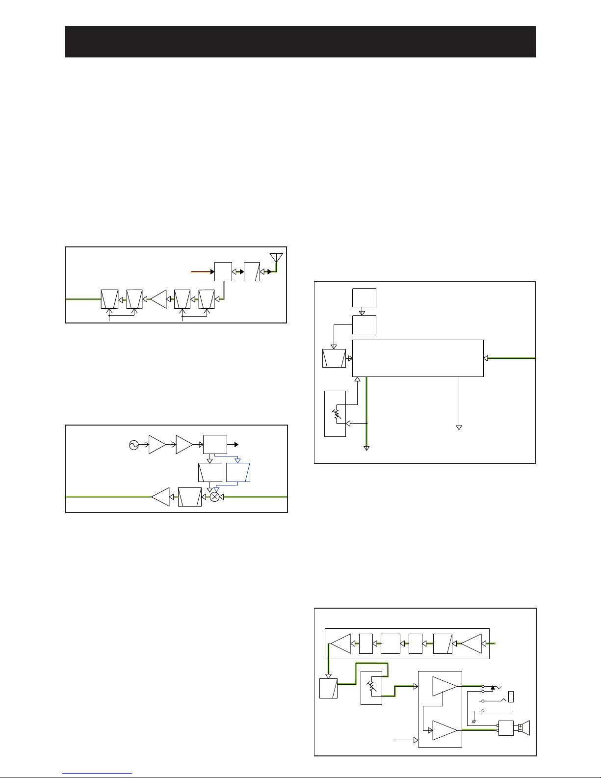
4-2 TRANSMIT CIRCUITS
TX AF CIRCUIT
The audio signal from the internal or external microphone
(MIC signal) is passed through the MIC gain SW (IC2) and
applied to the baseband IC (IC4).
The processed AF signal is passed through the AF
SW (IC2) and LPF (IC11), and then applied to the D/A
converter (IC10), which adjusts its level (=deviation). The
level-adjusted MIC signal is applied to the TX VCO as the
modulation signal.
MODULATION CIRCUIT
The modulation signal from the TX AF circuits is applied
to D13 of the TX VCO (Q27, D11 to D13 and D33). The
frequency-modulated signal from is amplified by two buffers
(Q30 and Q31), and then applied to the TX AMP circuit,
through the TX/RX SW (D16).
• TX AMPLIFIERS AND APC CIRCUIT
LPF
PWR
DET
D22,D23
ANT
SW
D19,D27
PWR
AM P
Q38
APC
AMP
IC17
DRIVE
AM P
Q36
ANT
From the
TX VCO
To the RX circuits
AMP
PRE
Q34
TX AMP CIRCUIT
The buffer amplified signal from the TX/RX SW (D16)
is sequentially amplified by the pre-AMP (Q34), drive
AMP (Q36) and power AMP (Q38). The power amplified TX
signal is passed through the antenna SW (D19) and LPF
(L29 to L31, C333, C347 to C350, C352 and C403), and
then applied to the antenna.
APC CIRCUITS
At the TX output power detector, the RF signal at the LPF
(L26, C303, C330, C353 and C355) is rectified by the
diodes (D22 and D23), and it is used as the TX power sens-
ing voltage.
The voltage is applied to the APC AMP (IC17), and the
output voltage controls the bias voltages of the drive AMP
(Q36) and power AMP (Q38) to keep the TX output power
constant.
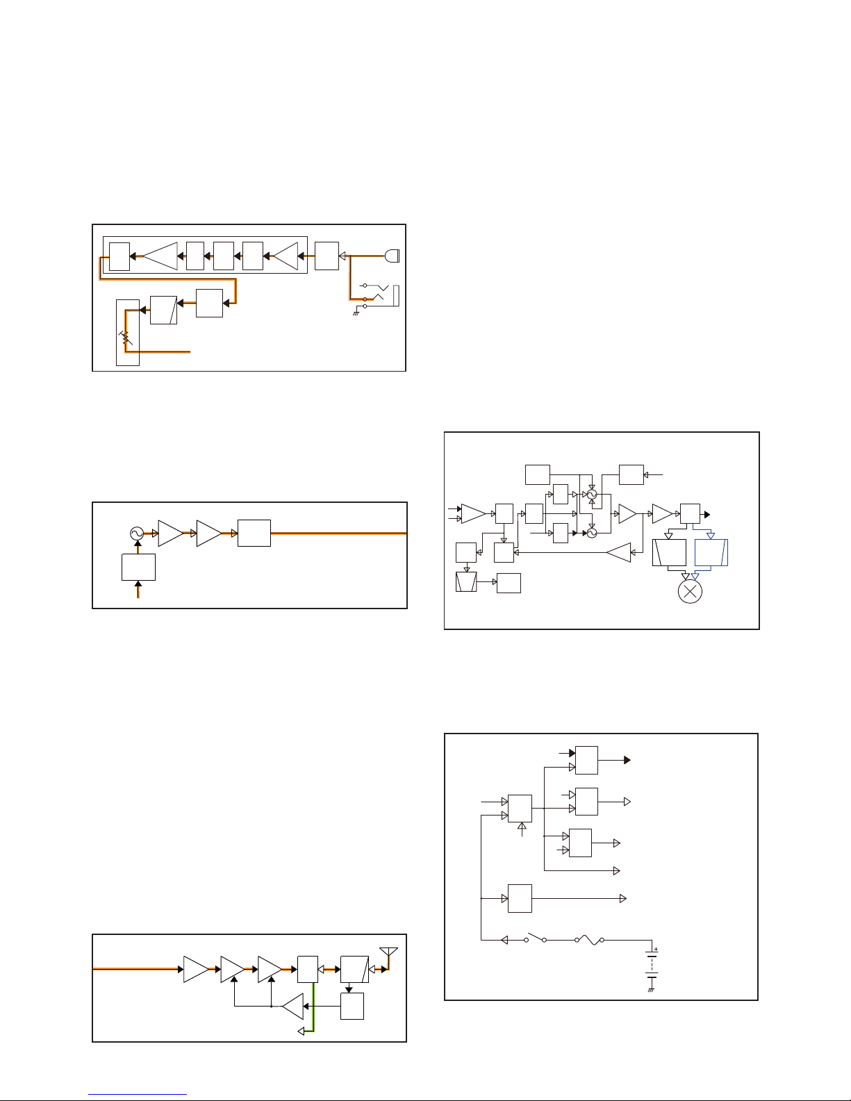
• FREQUENCY SYNTHESIZER CIRCUITS
4-4 VOLTAGE BLOCK DIAGRAM
1st IF mixer
TX/RX
SW
D16
D17
Q25
D9,D10
Q27
D11,D12
FIL
RIPPLE
Q23
VCO
SW
Q29
FIL
LOOP
PLL
IC IC15
X3
Q26
Q37
BPF
BUFF
Q31
BUFF
Q30
BUFF
Q32
X3
CR-794
TCXO
LV
ADJ
D11
LV
ADJ
D10
BUFF
IC7
IF IC
R5V
RX VCO
TX VCO
IC16
REF
BAL
15.3MHz
45.9MHz
LV
LVA
×2
To the TX AMPs
HPF** LPF*
To the TX circuits
To the RX circuits
To both RX and TX circuits
To the logical circuits
F1
12
T5
REG
Q17
REG
+5V
IC20
REG
S5
Q15
BATTERY_1
BT1
S5
REG
R5
Q16
CPU5
REG
IC6
S5C
VCC
R5C
+5V
T5C
S5V
R5VPWON
VCC
CPU5
T5V
4-3
FREQUENCY SYNTHESIZER CIRCUITS
The RX VCO is composed of Q25, D9, D10 and D32. The
output signal is amplified by two buffers (Q31 and Q31) and
applied to the 1st IF mixer (Q37), through the LO SW (D17)
and LO filter (LPF*: L41, C296 and C441, or HPF**: L21,
L42 and C293).
The TX VCO is composed of Q27, D11 to D13 and D33.
The output signal is amplified by two buffers (Q30 and Q31)
and applied to the pre-AMP (Q34), through the LO SW (D16).
A portion of oscillated VCO output signal from each VCO is
fed back to the PLL IC (IC15), through the buffer (Q32) and
LPF (L11, C210 and C231).
The applied VCO output signal is divided and phase-
compared with a 15.3 MHz reference frequency signal from
the TCXO (X3), which is also divided. The resulting signal
is output from the PLL IC (IC15), and DC-converted by the
loop filter, and then applied to the VCO as the lock voltage.
When the oscillation frequency drifts, its phase changes
from that of the reference frequency, causing a lock voltage
change to compensate for the drift in the VCO oscillating
frequency.
*:For [EUR] and [UK] versions.
**:For except [EUR] and [UK] versions.

4-4
PIN
NO.
LINE
NAME DESCRIPTION I/O
1 BEEP Beep audio (Square waves) to the AF
AMP (IC1). O
2 SENC 2/5 tone and DTMF encoding output. O
17 RMUT RX AF mute switch control.
L=During the squelch is closed. O
18 TMUT Transmission mute.
L=TX inhibit. O
19 MMUT MIC mute switch control.
L=MIC mute. O
20,
21
MGC1*,
MGC0* MIC gain control. O
22 CL0 Cloning data. O
23 CLI I
24 CSFT
CPU clock frequency shift control.
H=While the clock frequency is
shifted.
O
25 AUTX
Automatic TX control in the VOX
mode.
H=Microphone input is detected.
O
26 NWC
RX mode (narrow/wide) switching.
L=While receiving in the narrow
mode.
O
27 AFON AF power AMP control.
H=AF power AMP (IC55) is activated. O
28 SCK Common serial clock. O
29 S0 Common serial data. O
34 ESCL EEPROM clock. O
35 ESDA EEPROM data. I/O
36 DAST D/A converter strobe.
H=Load enable. O
37 PLST PLL IC strobe.
H=Load enable. O
38 R5C
Receive circuit power supply line
"R5" control.
H=While the receive circuit is
activated.
O
39 T5C
Transmit circuit power supply line
“T5V” control.
L=While transmitting.
O
40 S5C
TX/RX common circuit power supply
line "S5V" control.
L=While in the power save mode.
O
46 TLED TX LED indicator control.
L=While transmitting. O
47 RLED
RX LED Indicator control.
L=While receiving a signal or the
squelch is open.
O
48 LIGT LCD backlight control.
H=Lights. O
56,
57
CENC2,
CENC1 CTCSS/DTCS encoding output. O
58 DUSE AF LPF switching.
H=While sending the DTCS signal. O
59–
62
CBI0–
CBI3 [ROTARY SELECTOR] input. O
70 NOIS Noise level detect.
H=While receiving a signal. I
71 UNLK PLL unlock detect.
L=Unlocked. I
72 KR0 [P0], [1], [2] and [3] input.
L=Pushed. I
4-5 PORT ALLOCATIONS
• CPU (IC9)
PIN
NO.
LINE
NAME DESCRIPTION I/O
73 KR1 [P1], [4], [5] and [6] input.
L=Pushed. I
74 KR2 [P2], [7], [8] and [9] input.
L=Pushed. I
81 KR3 [P3], [*], [0] and [#] input.
L=Pushed. I
82 KS0 [P0], [P1], [P2] and [P3] input.
L=Pushed. I
83 KS1 [1], [4], [7] and [*] input.
L=Pushed. I
84 KS2 [2], [5], [8] and [0] input.
L=Pushed. I
85 KS3 [3], [6], [9] and [#] input.
L=Pushed. I
86 SDEC Decoded 2/5 tone and DTMF signals. I
87 CDEC Tone signal (CTCSS/DTCS) decoding
input. I
88 EPTT External PTT input.
H= An external PTT is pushed. I
89 IPTT [PTT] input.
L= Pushed. I
90 TEMP Transceiver temperature sensing
voltage. I
91 BATV Battery voltage. I
92 KRA [S1], [S2] and [EMER] input.
L= Pushed. I
93 SDEC2 Decoded 2/5 tone and DTMF signals. I
95 AFVI [VOLUME CONTROL] input. I
96 RSSI Input port for RSSI signal from the IF
IC (IC16, pin16). I
97 LVIN Lock voltage input. I
98 MDET External microphone connection
detect. I
99 VOXV Microphone input sensing voltage. I
*: MIC sensitivity setting.
Line name MGC0 MGC1 MIC sensitivity
Line state
H H 4 (Maximum)
LH 3
HL 2
L L 1 (Minimum)

5-1
SECTION 5
.
ADJUSTMENT PROCEDURE
MREQUIRED EQUIPMENTS
5-1 PREPARATION
MJIG CABLE
3-conductor 2.5 (d) mm plug
(MIC)
(GND)
33 k
3-conductor 3.5 (d) mm plug (CLONE) OPC-478UC
(GND)
(SP)
[JIG cable1]
[JIG cable2]
+−
AC MILLIVOLTMETER
(10 mV to 10 V)
AUDIO GENERATOR
(300–3000 Hz/1–500 mV)
+−
PTT
+
4.7 µF
EXTERNAL SPEAKER
(1 W/8 Ω)
+
−
SETTING;
Frequency : 1 kHz
Level :150 mV
Waveform : Sine wave
MCONNECTION
FM
deviation meter
to the antenna connector
Attenuator
30 dB
RF power meter
0.1– 10 W/50 Ω
Frequency
counter
Standard signal generator
–20 to 90 dBµ
(–127 to –17 dBm)
NEVER transmit while
an SSG is connected to
the antenna connector.
PC
to USB port
OPC-478UC
Speaker (8 Ω)
To [SP]
To [MIC]
(JIG cable 1)
(JIG cable 2)
IC-F1000/IC-F1000T/
IC-F1000S/IC-F1000T-T
To [SP] connector
EQUIPMENT GRADE AND RANGE EQUIPMENT GRADE AND RANGE
Cloning software CS-F2000 CLONING SOFTWARE
(Revision 1.0 or later) JIG cable Modified OPC-478UC
(See the illust below)
RF power meter
(50 terminated)
Measuring range : 0.1–10 W
Frequency range : 100–300 MHz
SWR : Less than 1.2 : 1
Frequency counter
Frequency range : 0.1–300 MHz
Frequency accuracy : ±1 ppm or better
Input level : Less than 1 mW
Modulation
Analyzer
Frequency range : 30–300 MHz
Measuring range : 0 to ±10 kHz Standard signal
generator (SSG)
Frequency range : 0.1–300 MHz
Output level : –20 to 90 dBµ
(–127 to –17 dBm)
AC millivoltmeter Measuring range : 10 mV to 10 V
Oscilloscope Frequency range : DC–20 MHz
Measuring range : 0.01–20 V Attenuator Power attenuation : 30 dB
Capacity : More than 10 W
Audio generator
(AG)
Frequency range : 300–3000 Hz
Output level : 1–500 mV External speaker Input impedance : 8
Capacity : More than 1 W

5-2
MADJUSTMENT CHANNELS
CONVENIENT: The same cloning file is available.
Right-click below, and select "Save Embeded File to
Disk."
For [EUR] versions:
When adjusting “FM DEVIATION” in the middle band, change the bandwidth to “Middle” as shown below.
Select “Middle”

5-3
CTCSS/DTCSS DEVIATION
Click to open the
“I/O Check window”
ADJUST CHANNEL
RX SENSITIVITY
RX SENSITIVITY
ADJUST CHANNEL
MODULATION BALANCE
MODULATION BALANCE
S-METER
REFERENCE FREQUENCY
SQUELCH
LOCK VOLTAGE
LOCK VOLTAGE
TX OUTPUT POWER
TX OUTPUT POWER
FM DEVIATION
FM DEVIATION
If the below window appears, the utility is password-protected.
Enter the password to open the "Adjust Utility" window.
NOTE: The above values for settings are example only.
Each transceiver has its own specific values for each setting.
MADJUSTMENT UTILITY

5-4
ADJUSTMENT TRANSCEIVER’S
CONDITION OPERATION ADJUSTMENT
ITEM VALUE
PLL LOCK
VOLTAGE
-Preparation-
1
–
1) Connect an RF power meter to the
antenna connector.
2) Set the preset adjustment value on the
adjustment utility window.
LV (RX LVA FL) 46
(0.9 V)
LV (TX LVA FL)
LV (RX LVA FH) 255
(5.0 V)
LV (TX LVA FH)
-ADJUSTMENT-
(RX Band low)
2•Select the item [RX LVA Start], then push [ENTER] to enter the
lock voltage adjustment mode. [RX LVA Start] –
3 • Channel: 1-1
• Receiving
• Select the item [RX LVA FL], then push
[ENTER]. [RX LVA FL] 0.9 V
4•Select the item [RX LVA Start], then push [ENTER]. [RX LVA Start] –
(RX Band high) 5 • Channel: 1-2
• Receiving
• Set the item adjustment value in the [RX
LVA FH] on the adjustment utility window,
then push [ENTER].
[RX LVA FH]
255
(5.0 V)
6•Select the item [RX LVA Start], then push [ENTER] to quit the
lock voltage adjustment mode. [RX LVA Start] –
-ADJUSTMENT-
(TX Band low)
7•Select the item [TX LVA Start], then push [ENTER] to enter the
lock voltage adjustment mode. [TX LVA Start] –
8 • Channel: 1-1
• Receiving
• Select the item [TX LVA FL], then push
[ENTER]. [TX LVA FL] 0.9 V
9•Select the item [TX LVA Start], then push [ENTER] to quit the
lock voltage adjustment mode. [TX LVA Start] –
(TX Band high) 10 • Channel: 1-2
• Receiving
• Set the item adjustment value in the [TX
LVA FH] on the adjustment utility window,
then push [ENTER].
[TX LVA FH]
255
(5.0 V)
11 • Select the item [TX LVA Start], then push [ENTER] to quit the
lock voltage adjustment mode. [TX LVA Start] –
PLL LOCK
VOLTAGE
-Verify-
(RX Band low)
1 • Channel: 1-3
• Receiving
• Click the [Reload (F5)] button to check on
the "I/O Check window" as below.
[LVIN]
(On the "I/O
Check window")
0.9 V ±0.2 V
(Verify)
(RX Band high) 2 • Channel: 1-4
• Receiving
Less than
3.5 V
(Verify)
(TX Band low) 3 • Channel: 1-3
• Transmitting
0.9 V ±0.2 V
(Verify)
(TX Band high) 4 • Channel: 1-4
• Transmitting
Less than
3.5 V
(Verify)
REFERENCE
FREQUENCY
1 • Channel: 1-5
• Transmitting
• Loosely couple a frequency counter to the
antenna connector. [REF]
174.000000
MHz
(±150 Hz)
5-2 FREQUENCY ADJUSTMENTS
1) Select an adjustment item using []/[] on the PC's keyboard.
2) Set or modify the adjustment value as specified using []/[] on the PC's keyboard, and then push [ENTER].
• I/O Check window
(The values shown above are only examples.
Each transceiver has own values.)
* * * Lock voltage

5-5
5-3 TRANSMIT ADJUSTMENTS
1) Select an adjustment item using []/[] on the PC’s keyboard.
2) Set or modify the adjustment value as specified using []/[]on the PC’s keyboard, and then push [ENTER].
ADJUSTMENT TRANSCEIVER’S
CONDITION OPERATION ADJUSTMENT
ITEM VALUE
TX OUTPUT
POWER
1 1) Connect an RF power meter to the antenna connector.
2) Select [Power Start], then push [ENTER] to enter the TX out-
put power adjustment mode.
[Power Start]
–
(High power,
Band low)
2 • Channel: 1-6
• Transmitting
1) Adjust the TX output power.
2) Select the item [Power Start], then
push [ENTER] to store the adjustment
value.
[Power (FL)] 5.0 W
(High power,
Band center)
3 • Channel: 1-7
• Transmitting
[Power (FC)]
(High power,
Band high)
4 • Channel: 1-8
• Transmitting [Power (FH)]
5•Select [Power Start], then push [ENTER] to quit the TX output
power adjustment mode. [Power Start] –
(L2 power,
Band low)
4 • Channel: 1-9
• Transmitting
• Adjust the TX output power. [Power (L2)] 2.0 W
(L1 power,
Band low)
5 • Channel: 1-10
• Transmitting [Power (L1)] 1.0 W
FM DEVIATION
-Narrow-
(Band low)
1 • Set [MIC gain] to “2” in the Set mode. [Mic Gain] 2
2•Connect a modulation analyzer with an oscilloscope to the an-
tenna connector through an attenuator, and set it as:
HPF: OFF
LPF: 15 kHz or 20 kHz
De-emphasis: OFF
Detector: (P–P)/2
• Connect an audio generator to the [MIC] jack through the JIG
cable, and set it as:
Frequency: 1 kHz
Waveform: Sine wave
Level: 150 mVrms
––
3•Select [MOD Start], then push [ENTER] to enter the TX output
power adjustment mode. [MOD Start] –
4 • Channel: 1-11
• Transmitting
1) Adjust the deviation.
2) Select [MOD Start], then push [EN-
TER] to store the adjustment value.
[MOD FL] ±2.10 ±0.05
kHz
(Band center) 5 • Channel: 1-12
• Transmitting [MOD FC]
(Band high) 6 • Channel: 1-13
• Transmitting [MOD FH]
7•Select [MOD Start], then push [ENTER] to quit the “FM DEVIA-
TION -Narrow-” adjustment mode. [MOD Start] –
FM DEVIATION
-Wide-*
1 • Channel: 1-14
• Transmitting
• Connect a modulation analyzer to
the antenna connector through an
attenuator, and set it as “FM DEVIA-
TION.”
• Connect an audio generator to the [MIC]
jack through the JIG cable, and set it as
“FM DEVIATION -Narrow-.”
[MOD W] ±4.10 ±0.05
kHz
FM DEVIATION
-Middle-**
2 • Channel: 1-14
• Transmitting
[MOD M]
±3.30 ±0.05
kHz
*: Except for [USA] versions. **: Only for [EUR] versions.

5-6
5-3 TRANSMIT ADJUSTMENTS (continued)
1) Select an adjustment item using []/[] on the PC’s keyboard.
2) Set or modify the adjustment value as specified using []/[] on the PC’s keyboard, and then push [ENTER].
ADJUSTMENT TRANSCEIVER’S
CONDITION OPERATION ADJUSTMENT
ITEM VALUE
MODULATION
BALANCE
1•Connect a modulation analyzer to the antenna connector
through an attenuator, and set it as “FM DEVIATION.”
––
2•Set BAL “BAL FL,” “BAL FC” and “BAL FH” to “90.” [BAL FL]
[BAL FC]
[BAL FH]
90
3•Set “MOD -Narrow-” to “255.” [MOD -Narrow-] 255
4•Select [BAL Start] to enter the “MODULATION BALANCE” ad-
justment mode. [BAL Start] –
(Band low) 5 • Channel: 1-15
• No MIC signal is ap-
plied.
• Transmitting
1) Adjust the deviation.
2) Select [BAL Start], then push [ENTER]
to store the adjustment value. [BAL FL]
±0.99 ±0.03
kHz
(Band center) 6 • Channel: 1-16
• Transmitting [BALFC] ±0.97 ±0.03
kHz
(Band high) 7 • Channel: 1-17
• Transmitting [BAL FH] ±1.00 ±0.03
kHz
8•Select [BAL Start] to quit the “MODULATION BALANCE” ad-
justment mode. [BAL Start] –
CTCSS/DTCS
DEVIATION
-Narrow-
1•Connect a modulation analyzer to the antenna connector
through an attenuator, and set it as “FM DEVIATION.” ––
2•Select [Tone Start] to enter the “CTCSS/DTCS DEVIATION”
adjustment mode. [Tone Start] –
(Band low) 3 • Channel: 1-18
• No MIC signal is ap-
plied.
• Transmitting
1) Adjust the deviation.
2) Select [Tone Start], then push [EN-
TER] to store the adjustment value. [Tone FL]
±0.35 ±0.05
kHz
(Band center) 4 • Channel: 1-19
• Transmitting [Tone FC]
(Band high) 5 • Channel: 1-20
• Transmitting [Tone FH]
6•Select [Tone Start] to quit the “CTCSS/DTCS DEVIATION” ad-
justment mode.[Tone Start] –
CTCSS/DTCS
DEVIATION
-Wide-*
1 • Channel: 1-21
• Transmitting
• Connect a modulation analyzer to
the antenna connector through an
attenuator, and set it as “FM DEVIA-
TION.”
[Tone W]
±0.70 ±0.05
kHz
CTCSS/DTCS
DEVIATION
-Middle-**
1 • Channel: 1-21
• Transmitting [Tone M]
±0.55 ±0.05
kHz
*: Except for [USA] versions. **: Only for [EUR] versions.

5-7
5-4 RECEIVE ADJUSTMENTS
1) Select an adjustment item using []/[] on the PC’s keyboard.
2) Set or modify the adjustment value as specified using []/[] on the PC’s keyboard, and then push [ENTER].
ADJUSTMENT TRANSCEIVER’S
CONDITION OPERATION ADJUSTMENT
ITEM VALUE
RECEIVE
SENSITIVITY
NOTE:
• “RECEIVE SENSITIVITY” must be adjusted before “S-METER.” Otherwise, “S-METER” will not be adjusted
properly. When “RECEIVE SENSITIVITY” is re-adjusted, “S-METER” must be also re-adjusted.
• Before the adjustment, turn OFF the Power save function.
1 • Set [SQL Level] to “2” in the Set mode. [SQL Level] 2
2• Connect an SSG to the antenna connector and set it as:
Level†: +30 dBµ (–77 dBm)
Modulation: 1 kHz
Deviation: ±3.0 kHz*
±1.5 kHz**
3•Select [BPF Start], then push [ENTER] to enter the “RECEIVE
SENSITIVITY” adjustment mode. [BPF Start] –
(T2 Band low) 4 • Channel: 1-22
• Receiving
1) Set the SSG as:
Frequency: 136 MHz
2) Select the item [BPF T2 FL], then push
[ENTER] to start the automatic adjustment.
3) Select the item [BPF Start], then push
[ENTER] to store the adjustment value.
[BPF T2 FL]
Push [ENTER]
(Automatic
adjustment)
(T1 Band low) 5 • Channel: 1-23
• Receiving
1) Select the item [BPF T1 FL], then push
[ENTER] to start the automatic adjustment.
2) Select the item [BPF Start], then push
[ENTER] to store the adjustment value.
[BPF T1 FL]
(T2 Band center) 6• Channel: 1-24
• Receiving
1) Set the SSG as:
Frequency: 155 MHz
2) Select the item [BPF T2 FC], then push
[ENTER] to start the automatic adjustment.
3) Select the item [BPF Start], then push
[ENTER] to store the adjustment value.
[BPF T2 FC]
(T1 Band center) 7• Channel: 1-25
• Receiving
1) Select the item [BPF T1 FC], then push
[ENTER] to start the automatic adjustment.
2) Select the item [BPF Start], then push
[ENTER] to store the adjustment value.
[BPF T1 FC]
(T2 Band high) 8• Channel: 1-26
• Receiving
1) Set the SSG as:
Frequency: 176 MHz
2) Select the item [BPF T2 FH], then push
[ENTER] to start the automatic adjustment.
3) Select the item [BPF Start], then push
[ENTER] to store the adjustment value.
[BPF T2 FH]
(T1 Band high) 9• Channel: 1-27
• Receiving
1) Select the item [BPF T1 FH], then push
[ENTER] to start the automatic adjustment.
2) Select the item [BPF Start], then push
[ENTER] to store the adjustment value.
[BPF T1 FH]
10 • Select [BPF Start], then push [ENTER] to quit the “RECEIVE SENSITIVITY” adjust-
ment mode.
–
†: The output level of the standard signal generator (SSG) is indicated as the 50 terminated.
*: Except for [USA] versions. **: For [USA] versions.

5-8
5-4 RECEIVE ADJUSTMENTS (continued)
1) Select an adjustment item using []/[] on the PC’s keyboard.
2) Set or modify the adjustment value as specified using []/[] on the PC’s keyboard, and then push [ENTER].
ADJUSTMENT TRANSCEIVER’S
CONDITION OPERATION ADJUSTMENT
ITEM VALUE
S-METER NOTE: When “RECEIVE SENSITIVITY” is re-adjusted, “S-METER” must be also re-adjusted.
1• Connect an SSG to the antenna connector and set it as:
Frequency: 155 MHz
Modulation: 1 kHz
Deviation: ±1.5 kHz
–
–
2•Select [RSSI] to enter the “RSSI” adjustment mode. [RSSI] –
(S3 Level) 3 • Channel: 1-28
• Receiving
• Set the SSG as:
Level†: +23 dBµ (–84 dBm) [RSSI]
Push [ENTER]
(Automatic
adjustment)
(S1 Level) 4 • Channel: 1-29
• Receiving
• Set the SSG as:
Level†: –7 dBµ (–114 dBm)
5•Select [RSSI] to quit the “RSSI” adjustment mode. [RSSI] –
SQUELCH NOTE: When “RECEIVE SENSITIVITY” is re-adjusted, “SQUELCH” must be also re-adjusted.
1 • Channel: 1-30
• Receiving
1) Connect an SSG to the antenna con-
nector and set it as:
Frequency: 136 MHz
Level†: –14 dBµ (–121 dBm)
Modulation: 1 kHz
Deviation: ±3.0 kHz
2) Once close the squelch by increasing the
[SQL] value, and then decrease the value
to open the squelch.
[SQL]
Squelch opens
(Push [ENTER]
to store the
value
)
†: The output level of the standard signal generator (SSG) is indicated as the 50 terminated.

Eqv.= This component is equivalent to the REF No. component listed above, and
may be substituted on parts orders and repairs.
6-1
SECTION 6.PARTS LIST
IC1 1110008450 S.IC ISD8102SYI T&R <MSK> T 94.1/14.7
IC2 1130015760 S.IC TC74VHC4066AFK(EK) T 78.1/31.6
IC3 1110008550 S.IC NJM2904CRB1-TE1-#HMZR T 84.2/23.8
IC4 1110007810 S.IC AK2346AP-L T 69.8/22.3
IC5 1110008550 S.IC NJM2904CRB1-TE1-#HMZR B 40.5/14.2
IC6 1180004430 S.REG XC6209F502MR-G B 33.2/11.4
IC7 1110008550 S.IC NJM2904CRB1-TE1-#HMZR B 50.7/29.0
IC8 1110007620 S.IC NJU7704F3-42A-TE1-#ZZZB B 9.0/10.2
IC9 1140016890 S.IC R4F20335RDFE B 19.1/14.2
IC10 1110007290 S.IC AK2330P-L B 57.1/21.9
IC11 1110008550 S.IC NJM2904CRB1-TE1-#HMZR B 57.5/28.5
IC13 1130016620 S.IC GT24C128A-2ZLI-TR <MSK> B 8.6/28.1
IC14 1130009581 S.IC TC7W66FU(TE12LF) B 25.6/33.7
IC15 1130017460 S.IC AK1542A-L B 19.5/35.9
IC16 1110008392 S.IC SC-1451A (AK2365AM-L) B 55.3/10.4
IC17 1110002751 S.IC TA75S01F(TE85RF) T 85.6/35.0
IC19 1180004430 S.REG XC6209F502MR-G T 100.0/23.3
IC20 1180004430 S.REG XC6209F502MR-G B 97.2/15.1
IC21 1130017430 S.IC NJU6434KS4-TE4-#ZZZB [#05] T 54.3/20.2
1130017430 S.IC NJU6434KS4-TE4-#ZZZB [#06]
1130017430 S.IC NJU6434KS4-TE4-#ZZZB [#07]
1130017430 S.IC NJU6434KS4-TE4-#ZZZB [#08]
1130017430 S.IC NJU6434KS4-TE4-#ZZZB [#09]
1130017430 S.IC NJU6434KS4-TE4-#ZZZB [#10]
1130017430 S.IC NJU6434KS4-TE4-#ZZZB [#11]
1130017430 S.IC NJU6434KS4-TE4-#ZZZB [#12]
1130017430 S.IC NJU6434KS4-TE4-#ZZZB [#13]
IC22 1190003700 S.IC KXCJ9-1008 B 8.0/34.6
IC23 1130014200 S.IC TC7WPB307FK(TE85LF) B 12.3/34.2
IC24 1180004140 S.REG XC6221A302MR-G B 12.5/30.1
Q1 1590004070 S.TRA LDTC144EET1G <SLVJ> B 65.6/41.3
Q2 1590004070 S.TRA LDTC144EET1G <SLVJ> T 78.8/35.8
Q3 1590004220 S.TRA DRA9123Y0L T 85.1/28.5
Q4 1590004070 S.TRA LDTC144EET1G <SLVJ> B 93.4/14.0
Q5 1590004390 S.TRA DMG504010R B 37.0/7.6
Q9 1520000910 S.TRA 2SB1132L-R-AB3-R <SLVJ> T 89.5/7.9
Q10 1590004590 S.TRA DMC506010R B 89.3/8.4
Q14 1560000841 S.FET 2SK1829(TE85RF) [#02] B 89.1/17.3
1560000841 S.FET 2SK1829(TE85RF) [#03]
1560000841 S.FET 2SK1829(TE85RF) [#06]
1560000841 S.FET 2SK1829(TE85RF) [#07]
1560000841 S.FET 2SK1829(TE85RF) [#10]
1560000841 S.FET 2SK1829(TE85RF) [#11]
Q15 1590003490 S.TRA DTA113ZE TL T 90.0/25.0
Q16 1590004310 S.TRA LDTA114EET1G <SLVJ> T 97.5/27.4
Q17 1590003490 S.TRA DTA113ZE TL B 100.3/28.0
Q19 1590004070 S.TRA LDTC144EET1G <SLVJ> B 51.6/34.1
Q20 1590004340 S.TRA DRC9144T0L B 6.7/21.0
Q21 1590004050 S.TRA LDTA144EET1G <SLVJ> T 103.0/22.9
Q22 1590004050 S.TRA LDTA144EET1G <SLVJ> T 102.6/25.7
Q23 1530002851 S.TRA 2SC4116-BL(TE85RF) B 40.3/18.4
Q24 1590004070 S.TRA LDTC144EET1G <SLVJ> B 39.6/39.6
Q25 1530002921 S.TRA 2SC4226-T1 Y25 (R25) B 42.5/27.9
Q27 1530002921 S.TRA 2SC4226-T1 Y25 (R25) B 42.5/35.3
Q28 1590004090 S.TRA LDTC114YET1G <SLVJ> B 32.8/39.6
Q29 1590004090 S.TRA LDTC114YET1G <SLVJ> B 35.2/39.7
Q30 1530003321 S.TRA 2SC5108-Y(TE85RF) B 36.5/23.0
Q31 1530003321 S.TRA 2SC5108-Y(TE85RF) B 40.5/23.9
Q32 1530003321 S.TRA 2SC5108-Y(TE85RF) B 32.1/22.9
Q33 1530003231 S.TRA 2SC5085-Y(TE85RF) [#01] B 57.7/6.5
1530002381 S.TRA 2SC4215-Y(TE85LF) [#02]
1530002381 S.TRA 2SC4215-Y(TE85LF) [#03]
1530003231 S.TRA 2SC5085-Y(TE85RF) [#04]
1530003231 S.TRA 2SC5085-Y(TE85RF) [#05]
1530002381 S.TRA 2SC4215-Y(TE85LF) [#06]
1530002381 S.TRA 2SC4215-Y(TE85LF) [#07]
1530003231 S.TRA 2SC5085-Y(TE85RF) [#08]
1530003231 S.TRA 2SC5085-Y(TE85RF) [#09]
1530002381 S.TRA 2SC4215-Y(TE85LF) [#10]
1530002381 S.TRA 2SC4215-Y(TE85LF) [#11]
1530003231 S.TRA 2SC5085-Y(TE85RF) [#12]
1530003231 S.TRA 2SC5085-Y(TE85RF) [#13]
Q34 1530003321 S.TRA 2SC5108-Y(TE85RF) B 54.5/36.7
Q36 1560001910 S.FET RD01MUS2B-T113 B 61.4/36.7
Q37 1580000731 S.FET 3SK293(TE85LF) B 69.4/18.1
Q38 1560001701 S.FET RD07MUS2B-T214 B 71.2/34.9
Q39 1580000731 S.FET 3SK293(TE85LF) B 84.5/15.8
Q40 1590004050 S.TRA LDTA144EET1G <SLVJ> T 90.0/32.1
Q41 1590004060 S.TRA LDTC114EET1G <SLVJ> [#05] B 23.5/24.8
1590004060 S.TRA LDTC114EET1G <SLVJ> [#06]
1590004060 S.TRA LDTC114EET1G <SLVJ> [#07]
1590004060 S.TRA LDTC114EET1G <SLVJ> [#08]
1590004060 S.TRA LDTC114EET1G <SLVJ> [#09]
1590004060 S.TRA LDTC114EET1G <SLVJ> [#10]
1590004060 S.TRA LDTC114EET1G <SLVJ> [#11]
1590004060 S.TRA LDTC114EET1G <SLVJ> [#12]
1590004060 S.TRA LDTC114EET1G <SLVJ> [#13]
Q42 1590004070 S.TRA LDTC144EET1G <SLVJ> B 90.4/13.0
Q44 1590004070 S.TRA LDTC144EET1G <SLVJ> B 8.3/37.4
D1 1790001860 S.VAR EZJZ0V80010 T 74.6/22.7
D4 1750001810 S.DIO L1SS400T1G <SLVJ> T 95.1/11.3
D5 1790001670 S.DIO RB706F-40T106 T 86.9/26.7
D6 1750001790 S.DIO 1SS390 TE61 B 8.0/18.7
D7 1750001820 S.DIO LRB706F-40T1G <SLVJ> B 4.4/20.8
REF PARTS DESCRIPTION M. H/V
NO. NO.
LOCATION
[MAIN UNIT]
M.=Mounted side (T: Mounted on the Top side, B: Mounted on the Bottom side)
S.=Surface mount
REF PARTS DESCRIPTION M. H/V
NO. NO.
LOCATION
[MAIN UNIT]
D9 1750001770 S.VAR 1SV323(TPH3F) B 31.5/26.7
D10 1750002860 S.VAR BBY57-02V H6327 <RYOYO> B 38.0/29.1
D11 1750002860 S.VAR BBY57-02V H6327 <RYOYO> B 35.3/31.5
D12 1750001770 S.VAR 1SV323(TPH3F) B 31.9/33.2
D13 1750001770 S.VAR 1SV323(TPH3F) B 37.4/31.6
D16 1750002990 S.DIO BAR88-02V H6327 <RYOYO> B 45.7/26.3
D17 1750002990 S.DIO BAR88-02V H6327 <RYOYO> B 46.3/23.8
D18 1720000701 S.VAR 1SV305(TPL3F) B 79.5/13.2
D19 1750002990 S.DIO BAR88-02V H6327 <RYOYO> B 83.9/36.0
D20 1750001810 S.DIO L1SS400T1G <SLVJ> T 89.9/34.3
D22 1790001790 S.DIO RB876W TL B 80.2/29.1
D23 1790001790 S.DIO RB876W TL B 82.4/29.1
D24 1750001810 S.DIO L1SS400T1G <SLVJ> [#02] B 90.1/19.8
1750001810 S.DIO L1SS400T1G <SLVJ> [#03]
1750001810 S.DIO L1SS400T1G <SLVJ> [#06]
1750001810 S.DIO L1SS400T1G <SLVJ> [#07]
1750001810 S.DIO L1SS400T1G <SLVJ> [#10]
1750001810 S.DIO L1SS400T1G <SLVJ> [#11]
D25 1750002860 S.VAR BBY57-02V H6327 <RYOYO> B 84.1/24.3
D27 1750002990 S.DIO BAR88-02V H6327 <RYOYO> B 86.2/27.7
D28 1750002990 S.DIO BAR88-02V H6327 <RYOYO> B 57.0/4.6
D29 1720000701 S.VAR 1SV305(TPL3F) B 82.9/13.2
D31 1750002860 S.VAR BBY57-02V H6327 <RYOYO> B 87.7/21.6
D32 1750001770 S.VAR 1SV323(TPH3F) B 32.8/26.7
D33 1750001770 S.VAR 1SV323(TPH3F) B 31.3/34.9
D34 1750001790 S.DIO 1SS390 TE61 T 64.5/14.5
D35 1790001860 S.VAR EZJZ0V80010 T 77.5/21.7
D36 1720000701 S.VAR 1SV305(TPL3F) [#02] B 80.7/13.2
1720000701 S.VAR 1SV305(TPL3F) [#03]
1720000701 S.VAR 1SV305(TPL3F) [#06]
1720000701 S.VAR 1SV305(TPL3F) [#07]
1720000701 S.VAR 1SV305(TPL3F) [#10]
1720000701 S.VAR 1SV305(TPL3F) [#11]
D37 1720000701 S.VAR 1SV305(TPL3F) [#02] B 80.8/10.7
1720000701 S.VAR 1SV305(TPL3F) [#03]
1720000701 S.VAR 1SV305(TPL3F) [#06]
1720000701 S.VAR 1SV305(TPL3F) [#07]
1720000701 S.VAR 1SV305(TPL3F) [#10]
1720000701 S.VAR 1SV305(TPL3F) [#11]
D38 1720000701 S.VAR 1SV305(TPL3F) [#02] B 79.6/10.7
1720000701 S.VAR 1SV305(TPL3F) [#03]
1720000701 S.VAR 1SV305(TPL3F) [#06]
1720000701 S.VAR 1SV305(TPL3F) [#07]
1720000701 S.VAR 1SV305(TPL3F) [#10]
1720000701 S.VAR 1SV305(TPL3F) [#11]
FI1 2030000870 S.MON MFT46.3P3 46.350 MHz
(FL-442) [#01] B 64.8/10.6
2030000150 S.MON DSF753SB 46.350 MHz
(FL-335) [#02]
2030000150 S.MON DSF753SB 46.350 MHz
(FL-335) [#03]
2030000870 S.MON MFT46.3P3 46.350 MHz
(FL-442) [#04]
2030000870 S.MON MFT46.3P3 46.350 MHz
(FL-442) [#05]
2030000150 S.MON DSF753SB 46.350 MHz
(FL-335) [#06]
2030000150 S.MON DSF753SB 46.350 MHz
(FL-335) [#07]
2030000870 S.MON MFT46.3P3 46.350 MHz
(FL-442) [#08]
2030000870 S.MON MFT46.3P3 46.350 MHz
(FL-442) [#09]
2030000150 S.MON DSF753SB 46.350 MHz
(FL-335) [#10]
2030000150 S.MON DSF753SB 46.350 MHz
(FL-335) [#11]
2030000870 S.MON MFT46.3P3 46.350 MHz
(FL-442) [#12]
2030000870 S.MON MFT46.3P3 46.350 MHz
(FL-442) [#13]
X1 6050013800 S.XTA CR-980 14.7456 MHz<SKD> T 64.7/19.3
X2 6050013790 S.XTA CR-981 19.6608 MHz<SKD> B 6.3/12.9
X3 6050013760 S.XTA CR-978 TTS18VSH 15.3 MHz B 47.2/17.2
L2 6200003640 S.COI MLF1608E 100K-T B 34.7/28.6
L3 6190002030 S.COI MLG1608S 1R0J-T B 36.8/28.6
L5 6200007170 S.COI MLF1608A 3R3K-T B 30.2/26.7
L6 6200008090 S.COI LQW2BHN68NJ03L B 36.5/26.5
L7 6200007760 S.COI LQW2BHN82NJ03L B 35.1/34.8
L9 6200012170 S.COI MLG1608S R18J-T B 52.8/18.0
L10 6200012170 S.COI MLG1608S R18J-T B 51.8/13.8
L11 6200007881 S.COI ELJRF 33NJFB B 26.8/25.8
L13 6200011031 S.COI ELJRF R10JFB [#01] B 38.6/23.7
6200011031 S.COI ELJRF R10JFB [#04]
6200011031 S.COI ELJRF R10JFB [#05]
6200011031 S.COI ELJRF R10JFB [#08]
6200011031 S.COI ELJRF R10JFB [#09]
6200011031 S.COI ELJRF R10JFB [#12]
6200011031 S.COI ELJRF R10JFB [#13]
L14 6200011031 S.COI ELJRF R10JFB B 43.3/23.5
L15 6200011031 S.COI ELJRF R10JFB B 32.1/24.4
L16 6200013800 S.COI MLK1005S39NJT B 55.1/38.2
Other manuals for IC-F1000 series
5
This manual suits for next models
3
Table of contents
Other Icom Transceiver manuals

Icom
Icom IC-751A User manual

Icom
Icom IC-7800 User manual

Icom
Icom IC-410PRO Setup guide

Icom
Icom IC-F5060 Series User manual

Icom
Icom IC-M45A User manual

Icom
Icom ID-51A User manual

Icom
Icom IC-7300 Installation instructions

Icom
Icom IC-M1EURO V User manual

Icom
Icom IA14 User manual

Icom
Icom CS-207 User manual
Popular Transceiver manuals by other brands

Nokia
Nokia NSM-5 SERIES Technical documentation

SAMCOM
SAMCOM FPEN10A user manual

Vertex Standard
Vertex Standard VX-160U Service manual

Siemens
Siemens PSO 4000 Quick reference guide

Verterx Standard
Verterx Standard Yaesu FTM-10R Technical supplement

Wulfsberg
Wulfsberg FLEXCOMM 2000 Series Operator's manual