Icom IC-M2A User manual

SERVICE
MANUAL
1-1-32, Kamiminami, Hirano-ku, Osaka, 547-0003, Japan S-13813IZ-C1-1
© 2001 Icom Inc.
VHF MARINE TRANSCEIVER

INTRODUCTION
DANGER
ORDERING PARTS
REPAIR NOTES
This service manual describes the latest service information
for the IC-M2A/IC-M21 VHF MARINE TRANSCEIVER at the
time of publication.
NEVER connect the transceiver to an AC outlet or to a DC
power supply that uses more than 10 V. This will ruin the
transceiver.
DO NOT expose the transceiver to rain, snow or any liquids.
DO NOT reverse the polarities of the power supply when con-
necting the transceiver.
DO NOT apply an RF signal of more than 20 dBm (100mW)
to the antenna connector. This could damage the transceiv-
er’s front end.
Be sure to include the following four points when ordering
replacement parts:
1. 10-digit order numbers
2. Component part number and name
3. Equipment model name and unit name
4. Quantity required
<SAMPLE ORDER>
1130007020 S.IC TC7S66FU IC-M2A MAIN UNIT 1 piece
8810004860 Screw PH M 2 x 6 ZK IC-M21 Chassis 10 pieces
Addresses are provided on the inside back cover for your
convenience.
1. Make sure a problem is internal before disassembling the transceiver.
2. DO NOT open the transceiver until the transceiver is disconnected from its power source.
3. DO NOT force any of the variable components. Turn them slowly and smoothly.
4. DO NOT short any circuits or electronic parts. An insulated turning tool MUST be used for all adjustments.
5. DO NOT keep power ON for a long time when the transceiver is defective.
6. DO NOT transmit power into a signal generator or a sweep generator.
7. ALWAYS connect a 40 dB to 50 dB attenuator between the transceiver and a deviation meter or spectrum analyzer when
using such test equipment.
8. READ the instructions of test equipment thoroughly before connecting equipment to the transceiver.
To upgrade quality, all electrical or mechanical parts and
internal circuits are subject to change without notice or oblig-
ation.
IC-M2A IC-M21
Model
IC-M2A
IC-M21
Version
U.S.A.
S.E.Asia
Europe
United Kingdom
Germany
Symbol
[USA]
[SEA]
[EUR]
[UK]
[FRG]
AC adapter
BC-147A
BC-147E
BC-147E
TX high power
5W
1W

TABLE OF CONTENTS
SECTION 1 SPECIFICATIONS
SECTION 2 INSIDE VIEWS
SECTION 3 DISASSEMBLY INSTRUCTIONS
SECTION 4 CIRCUIT DESCRIPTION
4-1 RECEIVER CIRCUITS . . . . . . . . . . . . . . . . . . . . . . . . . . . . . . . . . . . . . . . . . . . . . . . . . . . . .4-1
4-2 TRANSMITTER CIRCUITS . . . . . . . . . . . . . . . . . . . . . . . . . . . . . . . . . . . . . . . . . . . . . . . . .4-2
4-3 PLL CIRCUIT . . . . . . . . . . . . . . . . . . . . . . . . . . . . . . . . . . . . . . . . . . . . . . . . . . . . . . . . . . . .4-3
4-4 POWER SUPPLY CIRCUITS . . . . . . . . . . . . . . . . . . . . . . . . . . . . . . . . . . . . . . . . . . . . . . . .4-3
4-5 CPU PORT ALLOCATIONS . . . . . . . . . . . . . . . . . . . . . . . . . . . . . . . . . . . . . . . . . . . . . . . . .4-4
SECTION 5 ADJUSTMENT PROCEDURES
5-1 PREPARATION . . . . . . . . . . . . . . . . . . . . . . . . . . . . . . . . . . . . . . . . . . . . . . . . . . . . . . . . . .5-1
5-2 PLL AND TRANSMITTER ADJUSTMENTS . . . . . . . . . . . . . . . . . . . . . . . . . . . . . . . . . . . . .5-4
5-3 RECEIVER ADJUSTMENT . . . . . . . . . . . . . . . . . . . . . . . . . . . . . . . . . . . . . . . . . . . . . . . . . .5-5
SECTION 6 PARTS LIST
SECTION 7 MECHANICAL PARTS AND DISASSEMBLY
SECTION 8 SEMI-CONDUCTOR INFORMATION
SECTION 9 BOARD LAYOUTS
9-1 CHARGE UNIT (BC-150) . . . . . . . . . . . . . . . . . . . . . . . . . . . . . . . . . . . . . . . . . . . . . . . . . . .9-1
9-2 MAIN UNIT . . . . . . . . . . . . . . . . . . . . . . . . . . . . . . . . . . . . . . . . . . . . . . . . . . . . . . . . . . . . .9-2
9-3 VR UNIT . . . . . . . . . . . . . . . . . . . . . . . . . . . . . . . . . . . . . . . . . . . . . . . . . . . . . . . . . . . . . . .9-4
SECTION 10 BLOCK DIAGRAM
SECTION 11 VOLTAGE DIAGRAM
11-1 MAIN UNIT . . . . . . . . . . . . . . . . . . . . . . . . . . . . . . . . . . . . . . . . . . . . . . . . . . . . . . . . . . . . .11-1
11-2 VR UNIT . . . . . . . . . . . . . . . . . . . . . . . . . . . . . . . . . . . . . . . . . . . . . . . . . . . . . . . . . . . . . . .11-2

1 - 1
All stated specifications are subject to change without notice or obligation.
Frequencycoverage
Mode
Power supply requirement
Usable temperature
Frequency stability
at 5 W
at 3 W
at 1 W
at 0.5 W
at maximum audio
at stand-by
Antenna impedance
Dimensions
(Projections not included)
Weight
(with antenna and BP-224)
RF output power (at 7.2 V DC)
Modulation system
Max. frequency deviation
Frequency error
Spurious emissions
Adjacent channel power
Residual modulation
Audio harmonic distortion
Audio frequency response
Microphone impedance
Receive system
Intermediate frequencies
Sensitivity
Squelch sensitivity
Adjacent channel selectivity
Spurious response
Intermodulation
Hum and noise
Audio output power ( at 7.4 V)
Audio frequency response
IC-M2A IC-M21
RECEIVER TRANSMITTER GENERAL
Tx: 156.025 MHz–157.425 MHz Tx: 156.000 MHz–161.450 MHz
Rx: 156.025 MHz–163.275 MHz Rx: 156.000 MHz–163.425 MHz
16K0G3E (FM)
BP-224 (7.2 V DC)
–20 ˚C to +60 ˚C (–4˚F to +140˚F) –15 ˚C to +55 ˚C (+5˚F to +131˚F)
± 10 ppm ± 1.5 kHz
1.5 A
1.2 A
0.7 A
0.6 A [FRG] only
200 mA
20 mA
Type STUD / 50 Ω
61(W) ×135H) ×41(D) mm; 213⁄32(W) ×55⁄16(H) ×15⁄8(D) inch (with BP-224)
360 g; 12.7 oz (approx.)
Hi power; 5 W 5 W / 3 W / 1 W (High / Mid / Low) [OTHER]
Hi power; 1 W 1 W / 0.5 W (High / Low) [FRG]
Variable reactance frequency modulation
± 5.0 kHz
± 10 ppm ± 1.5 kHz
–65 dBc 250 nW
60 dB 70 dB
40 dB
Less than 10 % at 60 % deviation
+ 1 kHz to –3 dB of 6 dB octave from 300 Hz to 3000 Hz
2 kΩ
Double-conversion super heterodyne
1st: 21.70 MHz, 2nd: 450 kHz
0.25 µV at 12 dB SINAD 0.79 µV emf at 12 dB SINAD (typical)
0.35 µV 1.0 µV emf (typical)
70 dB (typical) 70 dB
70 dB (typical) 68 dB
40 dB
350 mW typical at 10 % distortion 200 mW at 10 % distortion
with an 8 Ωload with an 8 Ωload
–3 dB to +1 dB of –6 dB octave from 300 Hz to 3000 Hz
Current drain
(with BP-224)
Tx
Rx
SECTION 1 SPECIFICATIONS
Measurements made in accordance with TIA/EIA-603 or EN-301-178-2.

1 - 2
* Low power only
NOTE: Channels 3, 21, 23, 61, 64, 81, 82 and 83 CANNOT be used by the general public in USA waters.
CAN
21A
22A
23
24
25
26
27
28
60
61A
62A
64
64A
65A
66A*
67
68
69
70
71
72
CAN
73
74
77*
78A
79A
80A
81A
82A
83
83A
84
85
86
87
88
21b
25b
28b
83b
CAN
01
02
03
04A
05A
06
07A
08
09
10
11
12
13*
14
15*
16
17*
18A
19A
20*
21
‘‘VHF MARINE CHANNEL LIST (For IC-M2A)
USA
01A
03A
05A
06
07A
08
09
10
11
12
13*
14
15*
16
17*
18A
19A
20
20A
INT
01
02
03
04
05
06
07
08
09
10
11
12
13
14
15*
16
17
18
19
20
21
Transmit
156.050
156.050
156.100
156.150
156.150
156.200
156.200
156.250
156.250
156.300
156.350
156.350
156.400
156.450
156.500
156.550
156.600
156.650
156.700
156.750
156.800
156.850
156.900
156.900
156.950
156.950
157.000
157.000
157.050
Receive
160.650
156.050
160.700
160.750
156.150
160.800
156.200
160.850
156.250
156.300
160.950
156.350
156.400
156.450
156.500
156.550
156.600
156.650
156.700
156.750
156.800
156.850
161.500
156.900
161.550
156.950
161.600
157.000
161.650
USA
21A
22A
23A
24
25
26
27
28
61A
63A
64A
65A
66A
67*
68
69
70
71
72
INT
22
23
24
25
26
27
28
60
61
62
63
64
65
65A
66
66A
67
68
69
70
71
72
Transmit
157.050
157.100
157.100
157.150
157.150
157.200
157.250
157.300
157.350
157.400
156.025
156.075
156.075
156.125
156.125
156.175
156.175
156.225
156.225
156.275
156.275
156.325
156.325
156.375
156.425
156.475
Rx only
156.575
156.625
Receive
157.050
161.700
157.100
161.750
157.150
161.800
161.850
161.900
161.950
162.000
160.625
160.675
156.075
160.725
156.125
160.775
156.175
160.825
156.225
160.875
156.275
160.925
156.325
156.375
156.425
156.475
156.525
156.575
156.625
USA
73
74
77*
78A
79A
80A
81A
82A
83A
84
84A
85
85A
86
86A
87
87A
88
88A
INT
73
74
77
78
79
80
81
82
83
84
85
86
87
88
Transmit
156.675
156.725
156.875
156.925
156.925
156.975
156.975
157.025
157.025
157.075
157.075
157.125
157.125
157.175
157.175
157.225
157.225
157.275
157.275
157.325
157.325
157.375
157.375
157.425
157.425
Rx only
Rx only
Rx only
Rx only
Receive
156.675
156.725
156.875
161.525
156.925
161.575
156.975
161.625
157.025
161.675
157.075
161.725
157.125
161.775
157.175
161.825
157.225
161.875
157.275
161.925
157.325
161.975
157.375
162.025
157.425
161.650
161.850
162.000
161.775
Channel No. Frequency (MHz) Channel No. Frequency (MHz) Channel No. Frequency (MHz)
WX01
WX02
WX03
WX04
WX05
Transmit
Receive only
Receive only
Receive only
Receive only
Receive only
Receive
162.550
162.400
162.475
162.425
162.450
WX06
WX07
WX08
WX09
WX10
Transmit
Receive only
Receive only
Receive only
Receive only
Receive only
Receive
162.500
162.525
161.650
161.775
163.275
Frequency (MHz) Frequency (MHz)
Weather
channel Weather
channel
‘‘WX CHANNEL LIST ([IC-M2A] only)

1 - 3
* Low power only
‘‘VHF MARINE CHANNEL LIST (For IC-M21)
USA
01A
03A
05A
06
07A
08
09
10
11
12
13*
14
15*
16
17*
18A
19A
20
20A
21A
INT
01
02
03
04
05
06
07
08
09
10
11
12
13
14
15*
16
17
18
19
20
21
Transmit
156.050
156.050
156.100
156.150
156.150
156.200
156.250
156.250
156.300
156.350
156.350
156.400
156.450
156.500
156.550
156.600
156.650
156.700
156.750
156.800
156.850
156.900
156.900
156.950
156.950
157.000
157.000
157.050
157.050
Receive
160.650
156.050
160.700
160.750
156.150
160.800
160.850
156.250
156.300
160.950
156.350
156.400
156.450
156.500
156.550
156.600
156.650
156.700
156.750
156.800
156.850
161.500
156.900
161.550
156.950
161.600
157.000
161.650
157.050
USA
22A
23A
24
25
26
27
28
37A
61A
63A
64A
65A
66A
67*
68
69
70
71
72
73
INT
22
23
24
25
26
27
28
60
61
62
63
64
65
65A
66
66A
67
68
69
70
71
72
73
Transmit
157.100
157.100
157.150
157.150
157.200
157.250
157.300
157.350
157.400
157.850
156.025
156.075
156.075
156.125
156.175
156.175
156.225
156.225
156.275
156.275
156.325
156.325
156.375
156.425
156.475
Rx only
156.575
156.625
156.675
Receive
161.700
157.100
161.750
157.150
161.800
161.850
161.900
161.950
162.000
157.850
160.625
160.675
156.075
160.725
160.775
156.175
160.825
156.225
160.875
156.275
160.925
156.325
156.375
156.425
156.475
156.525
156.575
156.625
156.675
USA
74
77*
78A
79A
80A
81A
82A
83A
84
84A
85
85A
86
86A
87
87A
88
88A
INT
74
77
78
79
80
81
82
83
84
85
86
87
88
Transmit
156.725
156.875
156.925
156.925
156.975
156.975
157.025
157.025
157.075
157.075
157.125
157.125
157.175
157.175
157.225
157.225
157.275
157.275
157.325
157.325
157.375
157.375
157.425
157.425
Receive
156.725
156.875
161.525
156.925
161.575
156.975
161.625
157.025
161.675
157.075
161.725
157.125
161.775
157.175
161.825
157.225
161.875
157.275
161.925
157.325
161.975
157.375
162.025
157.425
Channel No. Frequency (MHz) Channel No. Frequency (MHz) Channel No. Frequency (MHz)

2 - 1
SECTION 2 INSIDE VIEWS
• MAIN UNIT
TOP VIEW BOTTOM VIEW
Antenna switching circuit
(D52: 1SV307)
Power amplifier
(Q54: 2SK2974)
APC
(IC50: NJM2125F)
IF amplifier
(Q151: 2SC2714 Y)
TX/RX switch
(D50, D51: MA77)
Antenna switching circuit
D90: 1SV307
D91: 1SS375
()
1st mixer
(Q150: 3SK272)
VCO circuit
IF DETECTOR IC
(IC170: TA31136FN)
PLL IC
(IC1: µPD3140GS)
D/A converter
(IC190: M62363FP-650C)
CPU
(IC360: HD6433844RA60H)
EEPROM
(IC340: HN58X2416TI)
Mic amplifier and
low pass filter circuits
(IC200: NJM2902V)

MAIN unit
Chassis
Earth plate H
H
H
I
I
H
I
I
3 - 1
SECTION 3 DISASSEMBLY INSTRUCTIONS
• Removing the Rear panel • Removing the Chassis unit
Rear panel
A
B
C
C
Rubber
Front panel
Front panel
Chassis unit
VR unit
E
G
D
F(Speaker connector)
¡Unscrew 1 screw, A (2 x 10 mm), and remove 1 washer, B.
™Unscrew 3 screws, C (2 x 8 mm).
£Remove the rear panel and rubber from the front panel.
¡Unscrew 1 nut, D.
™Unscrew 2 screws, E (2 x 6 mm).
£Take off the chassis unit in the direction of the arrow.
¢Unplug, F, to separate the front panel, J251, and the
chassis unit.
∞Remove 1 washer, G.
• Removing the MAIN unit
¡Unscrew 9 screws, H (2 x 4 mm).
™Unsolder 4 points, I, and remove earth plate.
£Separate the MAIN unit and the chassis.

4 - 1
4-1 RECEIVER CIRCUITS
4-1-1 ANTENNA SWITCHING CIRCUIT
(MAIN UNIT)
The antenna switching circuit functions as a low-pass filter
while receiving and as resonator circuit while transmitting.
The circuit does not allow transmit signals to enter receiver
circuits.
Received signals from the antenna connector pass through
the low-pass fileter (L80–L82, C80–C86) and antenna
switching circuit (D52, D90, D91). The filtered signals are
then applied to the RF amplifier circuit (Q90).
4-1-2 RF AND 1ST MIXER CIRCUITS (MAIN UNIT)
The 1st mixer circuit converts the received signals to a fixed
frequency of the 1st IF signal with a PLL output frequency.
By changing the PLL frequency, only the desired frequency
will be passed through a pair of crystal filters at the next
stage of the 1st mixer.
The signals from the antenna switching circuit are passed
through the tunable bandpass filter (D92, D93) and amplified
at the RF amplifier (Q90). The amplified signals are passed
through another tunable bandpass fileter (D130), and then
applied to the 1st mixer circuit (Q150).
The filtered signals are mixed at the 1st mixer (Q150) with a
1st LO signal coming from the PLL circuit to produce a 21.7
MHz 1st IF signal. The 1st IF signal is passed through two
crystal filters (FI150, FI151) and is then amplified at the IF
amplifier (Q151).
4-1-3 2ND IF AND DEMODULATOR CIRCUITS
(MAIN UNIT)
The 2nd mixer circuit converts the 1st IF signal to a 2nd IF
signal. A double convertion superheterodyne system (which
converts receive signal twice) improves the image rejection
and obtain stable receiver gain.
The 1st IF signal is applied to a 2nd mixer section of the FM
IF IC (IC170, pin 16). The signal is then mixed with a 2nd LO
signal for conversion into a 450 kHz 2nd IF signal.
IC170 contains the 2nd mixer, limiter amplifier, quadrature
detector and active filter circuits.A21.25 MHz 2nd LO signal
is produced at the PLL circuit using the reference frequency.
The 2nd IF signal from the 2nd mixer (IC170, pin 3) passes
through ceramic filters (FI170) to remove unwanted hetero-
dyned frequencies. It is then amplified at the limiter amplifi-
er section (IC170, pin 5) and applied to the quadrature
detector section (IC170, pins 10 and 11) to demodulate the
2nd IF signal into AF signals.
4-1-4 AF CIRCUIT (MAIN UNIT)
AF signals from the FM IF IC (IC170, pin 9) are fed to the
analog switch (IC260).
The AF signals (detected signals) are passed through the
analog switch (IC260, pins 2 and 1) and are then applied to
the active low-pass filter (IC200c, pin 9).
The filtered AF signals are applied to and adjusted audio
level at the [VOL] control (VR unit; R500). The level con-
trolled signals are passed through the AF mute switch
(Q280) which is controlled by “IVOLM” signal from the CPU
(IC9, pin 31). The passed signals are applied to the AF
power amplifier (IC280, pin 4), and then output to the inter-
nal speaker or [EXT SP] jack after being passed through the
de-emphasis circuit (R286, C285) to obtain the –6 dB/octave
frequency characteristics.
Mixer
16
IF amp.
2nd IF filter
450 kHz
PLL IC
IC1
X1
21.25 MHz
RSSI
IC170 TA31136FN(D)
14 "IF" (1st IF signal: 21.7 MHz)
from Q151
"RSSIV" signal to the CPU (pin 94)
11
10
9
87 5 3
217 16
Active
filter
FI170
Noise
detector
FM
detector Noise
comp.
"NOISV" signal to the CPU (pin 90)
12
C171
C174
R172
C176
C175
C180 C179
"SQLO" signal to the D/A
convertor IC (IC190, pin 15)
"SQLI" signal to the D/A
convertor IC (IC190, pin 16)
R175 R176 R174
AF signal "DET"
2nd
R171
X170
450 kHz R5V
R170
SECTION 4 CIRCUIT DESCRIPTION
• 2ND IF AND DEMODULATOR CIRCUITS

4 - 2
4-1-5 SQUELCH CIRCUIT (MAIN UNIT)
The noise squelch circuit cuts out AF signals when no RF
signals are received. By detecting noise components in the
AF signals, the squelch circuit switches the AF mute switch.
A portion of the AF signals divided by C175 from the FM IF
IC (IC170, pin 9) are applied to the D/Aconvertor (IC190, pin
16) to adjust amplitude. The signals from the D/A convertor
(IC190, pin 15) are applied to the active filter section (IC170,
pin 8). The active filter section amplifies and filters noise
components. The filtered signals are applied to the noise
detector section and output from IC170 (pin 14) as the
“NOISV” signal.
The “NOISV” signal from IC170 (pin 14) is applied to the
CPU (IC360, pin 90). The CPU compares the set squelch
level voltage and “NOISV” signal voltage to control the
squelch output.
4-2 TRANSMITTER CIRCUITS
4-2-1 MICROPHONE AMPLIFIER CIRCUIT
(MAIN UNIT)
The microphone amplifier circuit amplifies audio signals with
+6 dB/octave pre-emphasis characteristics from the micro-
phone to a level needed for the modulation circuit.
TheAF signals from the microphone are passed through the
pre-emphasis circuit (R253, C254) and are then applied to
the microphone amplifier (IC200b). The amplifiedAF signals
are applied to analog switch (IC260, pin 5).
The AF signals are amplified again at the limiter-amplifier
(IC200a) and then passed through the low-pass filter
(IC200d, pins 10 and 8). The filtered audio is applied to the
modulation circuit as the “MOD” signal.
4-2-2 MODULATION CIRCUIT (MAIN UNIT)
The modulation circuit modulates the VCO oscillating signal
(RF signal) using the microphone audio signals.
The audio signals “MOD” change the reactance of D22 and
D23 to modulate an oscillated signal at the VCO circuit
(Q21, Q22, D22, D23). The oscillated signal is amplified at
the buffer-amplifiers (Q23, Q24).
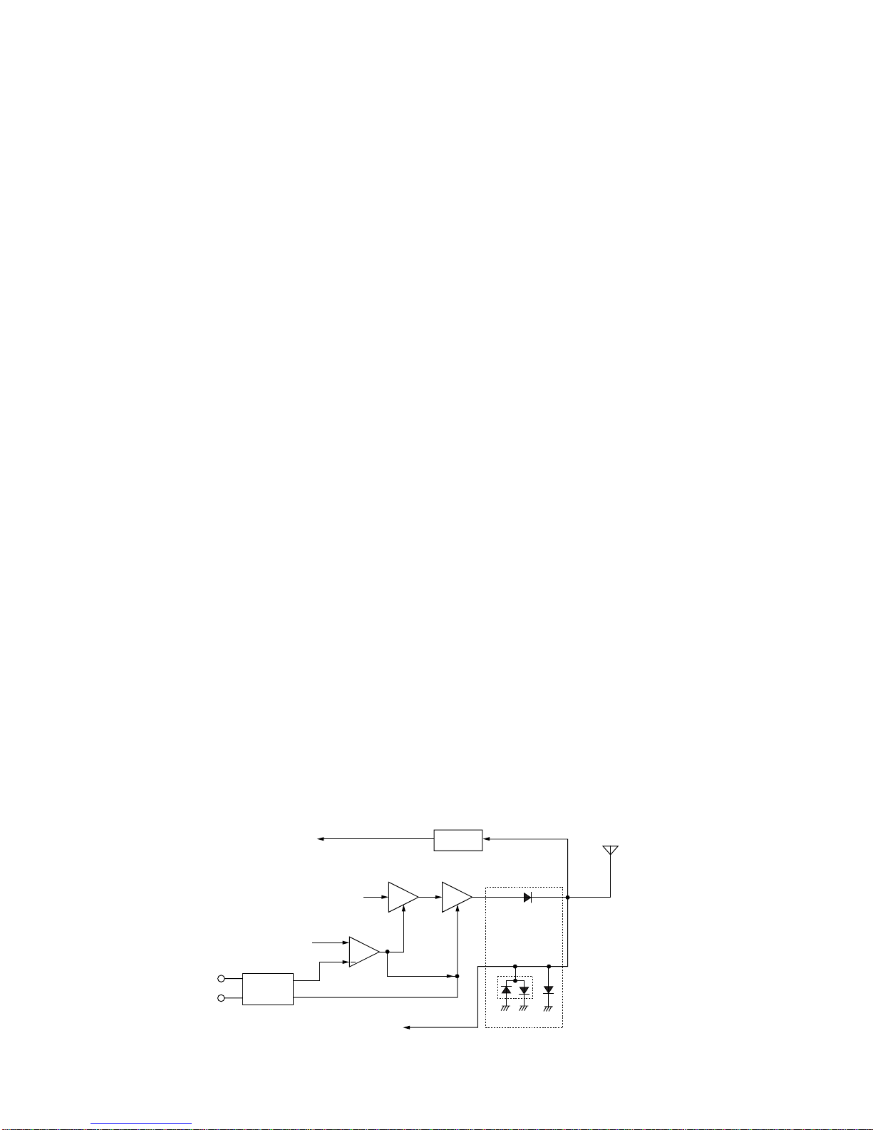
4-2-3 DRIVE/POWER AMPLIFIER CIRCUITS
(MAIN UNIT)
The signal from the VCO circuit passes through the trans-
mit/receive switching circuit (D50, D51) and is applied to the
buffer-amplifier (Q50). The amplified signal is amplified by
the pre-driver (Q53) and the power amplifier (Q54) to obtain
5 W of RF power (at 7.2 V). The amplified signal passes
through the antenna switching circuit (D52), and low-pass fil-
ter (L80–L82, C80–C86) and is then applied to the antenna
connector.
The bias current of the pre-driver (Q53) and the power
amplifier (Q54) is controlled by the APC circuit to stabilize
the output power.
4-2-4 APC CIRCUIT (MAIN UNIT)
The APC (Automatic Power Control) circuit provides stable
output power from the power amplifier even when the input
voltage or temperature changes, and selects HIGH, MID-
DLE or LOW (1W type selects HIGH or LOW) output power.
The APC circuit consists of a power detector and APC con-
trol circuits.
• POWER DETECTOR CIRCUIT (MAIN UNIT)
The power detector circuit (D80, C87) detects the transmit
output power level and converts it to DC voltage as the
“TDETV” signal. The detected signal is applied to the APC
control circuit.
• APC CONTROL CIRCUIT (MAIN UNIT)
The “TDETV” signal from the power detector circuit is
applied to the CPU (IC360, pin 92) to control the input volt-
age of the pre-driver (Q53) and the power amplifier (Q54).
When the output power changes, the CPU (IC360) outputs
APC control signal to the D/A converter (IC190). And then
“PCON” signal from the D/Aconverter controls theAPC con-
troller (IC50) to provide stable output power.
I. SENS
Q53
IC50
Q51, Q52
APC ctrl
To the 1st IF circuit
PWR amp.
Pre-Drive
D80, C87
Q54 D52
D91
Ant SW
Ant
D90
+
"PCON" signal
from IC190 (pin 3)
"TDETV" signal
to CPU (pin 92)
The amplified signal from the
buffer amplifier (Q50)
"VCC"
"T5V"
PWR det.
TX
RX
• APC CIRCUIT

4 - 3
4-3 PLL CIRCUIT (RF UNIT)
A PLL circuit provides stable oscillation of the transmit fre-
quency and receive 1st LO frequency. The PLL output com-
pares the phase of the divided VCO frequency to the refer-
ence frequency. The PLL output frequency is controlled by
the divided ratio (N-data) of a programmable divider.
The PLL circuit contains a VCO (Q21, Q22, D22, D23). The
oscillated signal is amplified at the buffer-amplifiers (Q23,
Q25) and then applied to the PLL IC (IC1, pin 19).
The PLL IC contains the prescalers, programmable counter,
programmable divider, phase selector and etc. The entered
signal is divided at the prescaler and programmable counter
sections by the N-data ratio from the CPU. The divided sig-
nal is detected on phase at the phase detector using the ref-
erence frequency.
If the oscillated signal drifts, the phase of its frequency
changes from the reference frequency, causing a lock volt-
age changes to compensate for the drift in the oscillated fre-
quency.
A portion of the VCO signal is amplified at buffer-amplifiers
(Q23, Q24) and is then applied to the receive 1st mixer
(Q150) or transmit buffer amplifier (Q50) via the TX/RX
switching diode (D50, D51).
Shift register
Prescaler
Phase
detector
Loop
filter
Programmable
counter
Programmable
divider
X1
21.25 MHz
"2nd LO" signal (21.25 MHz)
to the FM IF IC (IC170)
Q21, Q22, D22, D23
VCO
Buffer
Buffer
Buffer Q24
D50
D51
Q25
Q23
3
4
5PLST
IC1 (PLL IC)
SCK
SO
to transmitter circuit
to the 1st mixer circuit
17
16
13 19
LINE
HV
VCC
CPU5V
5V
R5V
V5V
T5V
DESCRIPTION
The voltage from the attached battery pack.
The same voltage as the HV line (battery volt-
age) which is controlled by the power switch (RF
unit; [OFF/VOL] control).
Common 5 V converted from the VCC line by the
CPU5V regulator circuit (IC220).
The output voltage is applied to the CPU (MAIN
unit; IC360), REG5V regulator, etc.
Common 5V converted from the VCC line by the
5V regulator circuit (Q223–Q225).
The output voltage is applied to the D/A convert-
er (IC190) and PLL IC (IC1), etc.
Receive 5V converted from the 5V line by the R5
regulator circuit (Q221).
The regulated voltage is applied to the MOD
MUTE circuit (Q20, D20, D21) and receiver cir-
cuit.
Common 5V converted from the 5V line by the
V5 regulator circuit (Q220).
The regulated voltage is applied to the VCO cir-
cuit
Transmit 5V converted from the 5V line by the T5
regulator circuit (Q222).
The regulated voltage is applied to the transmit-
ter circuit.
4-4 POWER SUPPLY CIRCUITS
VOLTAGE LINES
• PLL CIRCUIT

4 - 4
4-5 PORT ALLOCATIONS
4-5-1 CPU (IC360)
Pin
number
1
2
3
5
7
8
16
17
18
19
20
21
23
24
25
26
27
28
29
30
51
52
53
Port
name
LCDC1
LCDC2
BEEP
UNLK
BTYPE
BPFS
SCK
PLST
SDATA
DAST
LEDK
LEDL
ESDA
V5VS
T5VS
R5VS
AFVS
CLIN
CLOUT
IVOLM
HL
SQL
UP
Description
Outputs LCD contrast control signal.
Outputs beep audio signals.
Input port for unlock signal.
High : PLL is unlocked.
Input port for battery’s type and
cloning cable connecting detection.
Low : While alkaline cell battery is
used in the battery case.
Outputs RF band-pass filters control
signal.
High : While receiving below
159.990 MHz.
Low : While receiving above
160.000 MHz.
Outputs serial clock.
Outputs strobe signal to the PLL IC
(IC1, pin 3).
Outputs serial data.
Outputs strobe signal to the D/A con-
vertor IC (IC190, pin 6).
Outputs key pad back light control sig-
nal.
High : While key pad back light is
ON.
Outputs LCD back light control signal.
High : While LCD back light is ON.
I/O port for the EEPROM (IC340, pin
5) serial data signals.
Outputs the V5 regulator control sig-
nal.
Outputs the T5 regulator control sig-
nal.
Outputs the R5 regulator control sig-
nal.
Outputs the AF regulator control sig-
nal.
Input port for the cloning signal.
Outputs the cloning signal.
Output the speaker mute switch con-
trol signal.
High : While the AF output is muted.
Input port for the [H/L] key.
Low : While [H/L] key is pushed.
Input port for the [SQL] key.
Low : While [SQL] key is pushed.
Input port for the [Y] key.
Low : While [Y] key is pushed.
Pin
number
54
55
56
57
58
83
84
85
86
88
91
93
94
95
Port
name
DOWN
16CH
CHWX
SCAN
DW
5VS
MICM
DETM
WET
WXTV
BATTV
TEMPV
RSSIV
PTT
Description
Input port for the [Z] key.
Low : While [Z] key is pushed.
Input port for the [16] key.
Low : While [16] key is pushed.
Input port for the [CH/WX] key.
Low : While [CH/WX] key is pushed.
Input port for the [SCN] key.
Low : While [SCN] key is pushed.
Input port for the [DW] key.
Low : While [DW] key is pushed.
Outputs 5V regulator control signal.
Outputs the MIC mute switch control
signal.
Low : While muted.
Outputs the detector mute control sig-
nal.
Low : While muted.
Input port for transceiver’s internal
inundation detection.
Input port for WX tone detection.
Input port for the battery voltage
detection.
Input port for the transceiver’s internal
temperature detection.
Input port for the RSSI signal from the
FM IF IC (IC170, pin 12) to detect
receving signal strength.
Input port for the [PTT] switch.
High : While [PTT] switch is pushed.
4-5-2 D/A converter IC (IC190)
Pin
number
2
3
10
11
14
15
Port
name
FCON
PCON
MCON
BEPO
BEPST
SQLO
Description
Output signal to adjust the reference
frequency.
Output signal to adjust TX power.
Output signal to adjust modulation
while transmitting.
Output signal to adjust beep tone level
while “AUTO” is selected in set mode.
Output signal to adjust beep tone level
while 1–10 scale is selected in set
mode.
Output signal to adjust squelch level.

5 - 1
5-1 PREPARATION
■ENTERING THE ADJUSTMENT MODE
• Push and hold the [H/L] key and [PTT] switch, and then turn power ON.
■OPERATING IN THE ADJUSTMENT MODE
• Change adjustment items: [16] key
• Change adjustment values: [Y] and [Z] keys
■EXITING THE ADJUSTMENT MODE
When adjustment is finished, need to do follow operation to cancel the adjustment mode. Otherwise, the transceiver does not
work properly.
• Turn power OFF.
• Push and hold the [H/L] key and [PTT] switch, and then turn power ON.
EQUIPMENT
DC power supply
RF power meter
(terminated type)
Frequency counter
Digital multimeter
GRADE AND RANGE
Output voltage : 7.5 V DC
Current capacity : 3 A or more
Measuring range : 0.1–10 W
Frequency range : 100–300 MHz
Impedance : 50 Ω
SWR : Less than 1.2 : 1
Frequency range : 0.1–300 MHz
Frequency accuracy: ±1 ppm or better
Sensitivity : 100 mV or better
Input impedance : 10 MΩ/DC or better
EQUIPMENT
FM deviation meter
Audio generator
Standard signal
generator (SSG)
Attenuator
GRADE AND RANGE
Frequency range : 30–300 MHz
Measuring range : 0 to ±10 kHz
Frequency range : 300–3000 Hz
Measuring range : 1–500 mV
Frequency range : 100–300 MHz
Output level : 0.1 µV–32 mV
(–127 to –17 dBm)
Power attenuation : 40 dB or more
Capacity : 10 W or more
SECTION 5 ADJUSTMENT PROCEDURES
DC power supply
Top view Bottom view
connect (soldering) line here
++
connect (soldering) line here
• DC POWER CABLE CONNECTION

5 - 2
to the antenna connector
to [MIC] jack
Audio generator
Frequency
counter
CAUTION!
DO NOT transmit while
an SSG is connected to
the antenna connector.
AD-98FSC
Optional STUD-BNC
adapter
Attenuator
40 dB or 50 dB FM deviation meter
RF power meter
0.1 10 W/50
Standard signal generator
0.1 V to 32 mV
( 127 dBm to 17 dBm)
to [SP] jack
SINAD meter
Speaker (8 )
OPC-782
Optional plug adapter
cable
DETACHING/ATTACHING THE TOP PANEL
Detach the TOP PANEL with a
sharp point such as tweezers for
adjustment.
BE CAREFUL cracking the TOP
PANEL.
NOTE: If the tape on the back of the TOP PANEL has lost its
adhesion, replacement to a new one is necessary.
After adjustment, be sure to
reattach the TOP PANEL to
maintain the water resistance
capability.
CAUTION!
DO NOT detach the TOP PANEL
except for adjustment or cloning
to maintain the water resistance
capability.
• CONNECTION

5 - 3
5-2 PLL AND RX SENSITIVITY ADJUSTMENTS
LOCK
VOLTAGE
RX
SENSITIVITY
ADJUSTMENT
ADJUSTMENT ADJUSTMENT CONDITION MEASUREMENT VALUE POINT
UNIT LOCATION UNIT ADJUST
1
2
1
• Operating channel : ch16
• Receiving
• Operating channel : ch16
• Output power : Low
• Transmitting
• Operating channel : ch16
• Set an SSG as:
Frequency : 156.8 MHz
(ch. 16)
Level : 3.2 µV*
(–97 dBm)
Modulation : 1 kHz
Deviation : ±3.5 kHz
• Receiving
MAIN
Top
Panel
Connect a digital
multi-meter or oscil-
loscope to the
check point CP1.
Connect an SSG to
the antenna con-
nector and a SINAD
meter with 8 Ωload
to the [SP] jack.
1.8 V
1.7 V
0.35 µV (–116 dBm)
[M2A]
0.56 µV (–112 dBm)
[M21]
Verify
Verify
CP1
PLL lock voltage
check point
*The output level of the standard signal generator (SSG) is indicated as the SSG’s open circuit.

5 - 4
1
1
2
3
4
1
1
2
1
• Operating channel : ch16
• Output power : Low
• Connect an RF power meter or a 50 Ω
dummy load to the antenna connector.
• Transmitting
• Operating channel : ch16
• Output power : Hi
• Transmitting
• Output power : Mid.
• Transmitting
• Output power : Low
• Transmitting
• Output power : Extra-Low
• Transmitting
• Operating channel : ch16
• Output power : Low
• Connect an audio generator to the [MIC]
jack and set as:
1 kHz/25 mV
• Set an FM deviation meter as:
HPF : OFF
LPF : 20 kHz
De-emphasis : OFF
Detector : (P–P)/2
• Transmitting
• Operating channel : ch16
• Set an SSG as:
Frequency : 156.8 MHz
(ch. 16)
Level : 0.63 µV*
(–111 dBm)
Modulation : 1 kHz
Deviation : ±3.5 kHz
• Receiving
• Receving
• Operating channel : ch16
• Set an SSG as:
Frequency : 156.8 MHz
(ch. 16)
Level : 1 µV*
(–107 dBm)
Modulation : 1 kHz
Deviation : ±3.5 kHz
• Receiving
REFERENCE
FREQUENCY
[Fr]
OUTPUT
POWER
[Po H] (Hi)
[Po M] (Mid.)
[Po L] (Low)
[Po ML] (Extra-
Low)
FM
DEVIATION
[dE]
SQUELCH
LEVEL
[nL]
S-METER
[SL]
Top
Panel
Top
panel
Top
panel
Top
panel
Top
panel
Loosely couple the frequency
counter to the antenna connec-
tor.
Connect an RF power meter to
the antenna connector.
Connect an FM deviation meter
to the antenna connector
through an attenuator.
Connect an SSG to the antenna
connector and a SINAD meter
with 8 Ωload to the [SP] jack.
Connect an SSG to the antenna
connector and a SINAD meter
with 8 Ωload to the [SP] jack.
156.8000 MHz
5.0 W
3.0 W
0.8 W
0.45 W
±4.3 kHz
12 dB SINAD
At the point where
the signals just
appears.
Push [Y] or [Z] key,
then S-METER is
adjusted automati-
cally.
ADJUSTMENT ADJUSTMENT CONDITION MEASUREMENT VALUE
UNIT LOCATION
5-3 ADJUSTMENT MODE ADJUSTMENTS
Select an operation using [16] key, then set specified value using [Y] / [Z] keys on the transceiver’s front panel.
*The output level of the standard signal generator (SSG) is indicated as the SSG’s open circuit.

S.=Surface mount
R500 7210003130 VARIABLE TP76N97N-13F-10KA-2497
EP500 0910055331 PCB B 5715A
IC1 1130007610 S.IC µPD3140GS-E1 (DS8)
IC50 1120002830 S.IC NJM2125F-TE1
IC170 1110003200 S.IC TA31136FN (EL)
IC190 1190000350 S.IC M62363FP-650C
IC200 1110003780 S.IC NJM2902V-TE1
IC220 1110005350 S.IC NJM2870F05-TE1
IC260 1140003830 S.IC TC4W66F (TE12L)
IC280 1110001810 S.IC TA7368F (TP1)
IC340 1130010390 S.IC HN58X2416TI
IC341 1130009110 S.IC S-80942ANMP-DD6-T2
IC360 1140010410 S.IC HD6433844RA60H (FX-2497A)
Q20 1590000430 S.TRANSISTOR DTC144EUA T106
Q21 1530002920 S.TRANSISTOR 2SC4226-T1 R25
Q22 1530002920 S.TRANSISTOR 2SC4226-T1 R25
Q23 1530002600 S.TRANSISTOR 2SC4215-O (TE85R)
Q24 1530002600 S.TRANSISTOR 2SC4215-O (TE85R)
Q25 1530002600 S.TRANSISTOR 2SC4215-O (TE85R)
Q50 1530002920 S.TRANSISTOR 2SC4226-T1 R25
Q51 1530002060 S.TRANSISTOR 2SC4081 T106 R
Q52 1590002160 S.TRANSISTOR XP6401-(TX)
Q53 1560001020 S.FET 2SK2973 (MTS101P)
Q54 1560001050 S.FET 2SK2974
Q90 1530002920 S.TRANSISTOR 2SC4226-T1 R25
Q150 1580000660 S.FET 3SK272-(TX)
Q151 1530002360 S.TRANSISTOR 2SC2714-Y (TE85R)
Q220 1510000670 S.TRANSISTOR 2SA1588-GR (TE85R)
Q221 1510000670 S.TRANSISTOR 2SA1588-GR (TE85R)
Q222 1510000670 S.TRANSISTOR 2SA1588-GR (TE85R)
Q223 1590000430 S.TRANSISTOR DTC144EUA T106
Q224 1590001190 S.TRANSISTOR XP6501-(TX) .AB
Q225 1520000450 S.TRANSISTOR 2SB1132 T100 Q
Q230 1520000450 S.TRANSISTOR 2SB1132 T100 Q
Q231 1590001190 S.TRANSISTOR XP6501-(TX) .AB
Q240 1590001770 S.TRANSISTOR XP1213 (TX)
Q250 1590002530 S.TRANSISTOR UN911H (TX)
Q280 1530003090 S.TRANSISTOR 2SC4213-B (TE85R)
Q350 1590000660 S.TRANSISTOR DTC144TU T106
D1 1720000670 S.VARICAP HVU17TRF
D20 1790001260 S.DIODE MA2S077-(TX)
D21 1790000620 S.DIODE MA77 (TX)
D22 1720000780 S.VARICAP HVU350B TRF
D23 1720000780 S.VARICAP HVU350B TRF
D50 1790000620 S.DIODE MA77 (TX)
D51 1790000620 S.DIODE MA77 (TX)
D52 1790000580 S.DIODE 1SV307 (TPH3)
D80 1790001210 S.DIODE 1SS375-TL
D90 1790000580 S.DIODE 1SV307 (TPH3)
D91 1790001210 S.DIODE 1SS375-TL
D92 1790000620 S.DIODE MA77 (TX)
D93 1790000660 S.DIODE MA728 (TX)
D130 1790000620 S.DIODE MA77 (TX)
D350 1750000130 S.DIODE DA204U T106
FI150 2010002570 XTAL FL-346 (21.700 MHz)
FI151 2010002570 XTAL FL-346 (21.700 MHz)
FI170 2020001270 CERAMIC CFWLB450KE2A-B0 (CFWM450E)
X1 6050011350 S.XTAL CR-726 (21.250 MHz)
X170 6070000190
S.DISCRIMINATOR
CDBCB450KCAY24-R0
X360 6050010290 S.XTAL CR-610 (7.9872 MHz)
L1 6200008070 S.COIL MLF1608E 6R8K 6.8U
L20 6200007000 S.COIL ELJRE 82NG-F
L21 6200003090 S.COIL NL 322522T-2R7J-3
L22 6200008190 S.COIL 0.25-1.9-8TL 80N
L23 6200006980 S.COIL ELJRE R10G-F
L24 6200006980 S.COIL ELJRE R10G-F
L25 6200006980 S.COIL ELJRE R10G-F
L49 6200005740 S.COIL ELJRE 47NG-F
L50 6200006980 S.COIL ELJRE R10G-F
L51 6200007000 S.COIL ELJRE 82NG-F
L52 6200010230 S.COIL EXCCL3216U1
L53 6200002330 S.COIL LQN 1A 15NJ04
L54 6200010230 S.COIL EXCCL3216U1
L55 6200009240 S.COIL 0.20-1.0-7TL 31N
L56 6200008530 S.COIL 0.30-1.0-4TL 12N
L57 6200008400 S.COIL 0.35-1.6-6TL 36N
L58 6200003710 S.COIL NL 252018T-2R7J
L80 6200008450 S.COIL 0.35-1.6-5TL 28N
L81 6200008450 S.COIL 0.35-1.6-5TL 28N
L82 6200008400 S.COIL 0.35-1.6-6TL 36N
L90 6200008150 S.COIL 0.35-1.6-7TL 44N
L91 6200007760 S.COIL LQN21A 82NJ04
L92 6200007760 S.COIL LQN21A 82NJ04
L93 6200008190 S.COIL 0.25-1.9-8TL 80N
L94 6200008190 S.COIL 0.25-1.9-8TL 80N
L95 6200004720 S.COIL MLF1608D R10K-T
L120 6200002430 S.COIL NL 252018T-082J
L121 6200002410 S.COIL NL 252018T-056J
L122 6200003550 S.COIL MLF1608A 4R7K-T
L130 6200007760 S.COIL LQN21A 82NJ04
L131 6200007760 S.COIL LQN21A 82NJ04
L132 6200008190 S.COIL 0.25-1.9-8TL 80N
L133 6200008190 S.COIL 0.25-1.9-8TL 80N
L150 6200003680 S.COIL LQN 1N R82M
R1 7510001160 S.THERMISTOR NTCCM1608 4LH 473KC
R2 7030003940 S.RESISTOR ERJ3GEYF 104 V (100 kΩ)
R3 7030003560 S.RESISTOR ERJ3GEYJ 103 V (10 kΩ)
R4 7030003640 S.RESISTOR ERJ3GEYJ 473 V (47 kΩ)
R5 7030003380 S.RESISTOR ERJ3GEYJ 331 V (330 Ω)
R6 7030003440 S.RESISTOR ERJ3GEYJ 102 V (1 kΩ)
R7 7030003640 S.RESISTOR ERJ3GEYJ 473 V (47 kΩ)
R8 7030003440 S.RESISTOR ERJ3GEYJ 102 V (1 kΩ)
R9 7030003200 S.RESISTOR ERJ3GEYJ 100 V (10 Ω)
R10 7030003480 S.RESISTOR ERJ3GEYJ 222 V (2.2 kΩ)
R20 7030003320 S.RESISTOR ERJ3GEYJ 101 V (100 Ω)
R22 7030003410 S.RESISTOR ERJ3GEYJ 561 V (560 Ω)
R23 7030003440 S.RESISTOR ERJ3GEYJ 102 V (1 kΩ)
R24 7030003680 S.RESISTOR ERJ3GEYJ 104 V (100 kΩ)
R25 7030003680 S.RESISTOR ERJ3GEYJ 104 V (100 kΩ)
R26 7030003550 S.RESISTOR ERJ3GEYJ 822 V (8.2 kΩ)
R27 7030003550 S.RESISTOR ERJ3GEYJ 822 V (8.2 kΩ)
R28 7030003350 S.RESISTOR ERJ3GEYJ 181 V (180 Ω)
R29 7030003390 S.RESISTOR ERJ3GEYJ 391 V (390 Ω)
R30 7030003660 S.RESISTOR ERJ3GEYJ 683 V (68 kΩ)
R31 7030003420 S.RESISTOR ERJ3GEYJ 681 V (680 Ω)
R32 7030003390 S.RESISTOR ERJ3GEYJ 391 V (390 Ω)
R33 7030003630 S.RESISTOR ERJ3GEYJ 393 V (39 kΩ)
R34 7030003400 S.RESISTOR ERJ3GEYJ 471 V (470 Ω)
R35 7030003660 S.RESISTOR ERJ3GEYJ 683 V (68 kΩ)
R36 7030003440 S.RESISTOR ERJ3GEYJ 102 V (1 kΩ)
R50 7030003440 S.RESISTOR ERJ3GEYJ 102 V (1 kΩ)
R52 7030003520 S.RESISTOR ERJ3GEYJ 472 V (4.7 kΩ)
R53 7030003320 S.RESISTOR ERJ3GEYJ 101 V (100 Ω)
R54 7030003260 S.RESISTOR ERJ3GEYJ 330 V (33 Ω)
R55 7030003500 S.RESISTOR ERJ3GEYJ 332 V (3.3 kΩ)
R56 7030003450 S.RESISTOR ERJ3GEYJ 122 V (1.2 kΩ)
R57 7030003310 S.RESISTOR ERJ3GEYJ 820 V (82 Ω)
R58 7030003440 S.RESISTOR ERJ3GEYJ 102 V (1 kΩ)
R59 7030003580 S.RESISTOR ERJ3GEYJ 153 V (15 kΩ)
6 - 1
SECTION 6 PARTS LIST
REF ORDER DESCRIPTION
NO. NO.
[VR UNIT] REF ORDER DESCRIPTION
NO. NO.
[MAIN UNIT]
REF ORDER DESCRIPTION
NO. NO.
[MAIN UNIT]

6 - 2
S.=Surface mount
R60 7030003440 S.RESISTOR ERJ3GEYJ 102 V (1 kΩ)
R61 7030007330 S.RESISTOR ERJ1WRSJR15U (0.15 Ω)
R62 7030003680 S.RESISTOR ERJ3GEYJ 104 V (100 kΩ)
R63 7030003560 S.RESISTOR ERJ3GEYJ 103 V (10 kΩ)
R64 7030003560 S.RESISTOR ERJ3GEYJ 103 V (10 kΩ)
R65 7030003680 S.RESISTOR ERJ3GEYJ 104 V (100 kΩ)
R66 7030003740 S.RESISTOR ERJ3GEYJ 334 V (330 kΩ)
R67 7030003680 S.RESISTOR ERJ3GEYJ 104 V (100 kΩ)
R68 7030003320 S.RESISTOR ERJ3GEYJ 101 V (100 Ω)
R69 7030003580 S.RESISTOR ERJ3GEYJ 153 V (15 kΩ)
R70 7030003580 S.RESISTOR ERJ3GEYJ 153 V (15 kΩ)
R71 7030003320 S.RESISTOR ERJ3GEYJ 101 V (100 Ω)
R72 7030003280 S.RESISTOR ERJ3GEYJ 470 V (47 Ω)
R73 7030003440 S.RESISTOR ERJ3GEYJ 102 V (1 kΩ)
R74 7030003560 S.RESISTOR ERJ3GEYJ 103 V (10 kΩ)
R75 7030003320 S.RESISTOR ERJ3GEYJ 101 V (100 Ω)
R76 7030000280 S.RESISTOR MCR10EZHJ 150 Ω(151)
R80 7030003670 S.RESISTOR ERJ3GEYJ 823 V (82 kΩ)
R81 7030003600 S.RESISTOR ERJ3GEYJ 223 V (22 kΩ)
R82 7030003510 S.RESISTOR ERJ3GEYJ 392 V (3.9 kΩ)
R90 7030003560 S.RESISTOR ERJ3GEYJ 103 V (10 kΩ)
R91 7030003440 S.RESISTOR ERJ3GEYJ 102 V (1 kΩ)
R93 7030003440 S.RESISTOR ERJ3GEYJ 102 V (1 kΩ)
R94 7030003620 S.RESISTOR ERJ3GEYJ 333 V (33 kΩ)
R95 7030003320 S.RESISTOR ERJ3GEYJ 101 V (100 Ω) [M2A]
7030003280 S.RESISTOR ERJ3GEYJ 470 V (47 Ω) [M21]
R96 7030003360 S.RESISTOR ERJ3GEYJ 221 V (220 Ω) [M2A]
7030003320 S.RESISTOR ERJ3GEYJ 101 V (100 Ω) [M21]
R115 7030003270 S.RESISTOR ERJ3GEYJ 390 V (39 Ω) [M21] only
R120 7030003480 S.RESISTOR ERJ3GEYJ 222 V (2.2 kΩ)
R121 7030003560 S.RESISTOR ERJ3GEYJ 103 V (10 kΩ)
R130 7030003560 S.RESISTOR ERJ3GEYJ 103 V (10 kΩ)
R131 7030003440 S.RESISTOR ERJ3GEYJ 102 V (1 kΩ)
R132 7030003560 S.RESISTOR ERJ3GEYJ 103 V (10 kΩ)
R133 7030003560 S.RESISTOR ERJ3GEYJ 103 V (10 kΩ)
R134 7030003300 S.RESISTOR ERJ3GEYJ 680 V (68 Ω)
R150 7030003320 S.RESISTOR ERJ3GEYJ 101 V (100 Ω)
R151 7030003500 S.RESISTOR ERJ3GEYJ 332 V (3.3 kΩ)
R152 7030003460 S.RESISTOR ERJ3GEYJ 152 V (1.5 kΩ)
R153 7030003460 S.RESISTOR ERJ3GEYJ 152 V (1.5 kΩ)
R154 7030003680 S.RESISTOR ERJ3GEYJ 104 V (100 kΩ)
R155 7030003460 S.RESISTOR ERJ3GEYJ 152 V (1.5 kΩ)
R156 7030003400 S.RESISTOR ERJ3GEYJ 471 V (470 Ω)
R170 7030003390 S.RESISTOR ERJ3GEYJ 391 V (390 Ω)
R171 7030003450 S.RESISTOR ERJ3GEYJ 122 V (1.2 kΩ)
R172 7030003400 S.RESISTOR ERJ3GEYJ 471 V (470 Ω)
R173 7030003460 S.RESISTOR ERJ3GEYJ 152 V (1.5 kΩ)
R174 7030003720 S.RESISTOR ERJ3GEYJ 224 V (220 kΩ)
R175 7030003640 S.RESISTOR ERJ3GEYJ 473 V (47 kΩ)
R176 7030003540 S.RESISTOR ERJ3GEYJ 682 V (6.8 kΩ)
R192 7030003390 S.RESISTOR ERJ3GEYJ 391 V (390 Ω)
R193 7030003400 S.RESISTOR ERJ3GEYJ 471 V (470 Ω)
R194 7030003680 S.RESISTOR ERJ3GEYJ 104 V (100 kΩ)
R201 7030003580 S.RESISTOR ERJ3GEYJ 153 V (15 kΩ)
R202 7030003680 S.RESISTOR ERJ3GEYJ 104 V (100 kΩ)
R203 7030003810 S.RESISTOR ERJ3GEYJ 125 V (1.2 MΩ)
R204 7030003520 S.RESISTOR ERJ3GEYJ 472 V (4.7 kΩ)
R205 7030003610 S.RESISTOR ERJ3GEYJ 273 V (27 kΩ)
R206 7030003590 S.RESISTOR ERJ3GEYJ 183 V (18 kΩ)
R207 7030003610 S.RESISTOR ERJ3GEYJ 273 V (27 kΩ)
R212 7030003460 S.RESISTOR ERJ3GEYJ 152 V (1.5 kΩ)
R213 7030003660 S.RESISTOR ERJ3GEYJ 683 V (68 kΩ)
R214 7030003580 S.RESISTOR ERJ3GEYJ 153 V (15 kΩ)
R220 7030003560 S.RESISTOR ERJ3GEYJ 103 V (10 kΩ)
R221 7030003520 S.RESISTOR ERJ3GEYJ 472 V (4.7 kΩ)
R222 7030003560 S.RESISTOR ERJ3GEYJ 103 V (10 kΩ)
R223 7030003520 S.RESISTOR ERJ3GEYJ 472 V (4.7 kΩ)
R224 7030003560 S.RESISTOR ERJ3GEYJ 103 V (10 kΩ)
R225 7030003520 S.RESISTOR ERJ3GEYJ 472 V (4.7 kΩ)
R226 7030003480 S.RESISTOR ERJ3GEYJ 222 V (2.2 kΩ)
R227 7030003560 S.RESISTOR ERJ3GEYJ 103 V (10 kΩ)
R228 7030003600 S.RESISTOR ERJ3GEYJ 223 V (22 kΩ)
R230 7030003610 S.RESISTOR ERJ3GEYJ 273 V (27 kΩ)
R231 7030003800 S.RESISTOR ERJ3GEYJ 105 V (1 MΩ)
R232 7030003440 S.RESISTOR ERJ3GEYJ 102 V (1 kΩ)
R233 7030003480 S.RESISTOR ERJ3GEYJ 222 V (2.2 kΩ)
R234 7030003500 S.RESISTOR ERJ3GEYJ 332 V (3.3 kΩ)
R235 7030005930 S.RESISTOR ERJ3GEYF 334 V (330 kΩ)
R236 7030008090 S.RESISTOR ERJ3EKF 1503 V (150 kΩ)
R240 7030003340 S.RESISTOR ERJ3GEYJ 151 V (150 Ω)
R241 7030003430 S.RESISTOR ERJ3GEYJ 821 V (820 Ω)
R242 7030003430 S.RESISTOR ERJ3GEYJ 821 V (820 Ω)
REF ORDER DESCRIPTION
NO. NO.
[MAIN UNIT]
R245 7030003440 S.RESISTOR ERJ3GEYJ 102 V (1 kΩ)
R250 7030003680 S.RESISTOR ERJ3GEYJ 104 V (100 kΩ)
R251 7030003400 S.RESISTOR ERJ3GEYJ 471 V (470 Ω)
R252 7030003620 S.RESISTOR ERJ3GEYJ 333 V (33 kΩ)
R253 7030003480 S.RESISTOR ERJ3GEYJ 222 V (2.2 kΩ)
R255 7030003700 S.RESISTOR ERJ3GEYJ 154 V (150 kΩ)
R256 7030003590 S.RESISTOR ERJ3GEYJ 183 V (18 kΩ)
R257 7030003520 S.RESISTOR ERJ3GEYJ 472 V (4.7 kΩ)
R258 7030003520 S.RESISTOR ERJ3GEYJ 472 V (4.7 kΩ)
R260 7030003570 S.RESISTOR ERJ3GEYJ 123 V (12 kΩ)
R261 7030003510 S.RESISTOR ERJ3GEYJ 392 V (3.9 kΩ)
R262 7030003470 S.RESISTOR ERJ3GEYJ 182 V (1.8 kΩ)
R263 7030003680 S.RESISTOR ERJ3GEYJ 104 V (100 kΩ)
R264 7030003680 S.RESISTOR ERJ3GEYJ 104 V (100 kΩ)
R265 7030003680 S.RESISTOR ERJ3GEYJ 104 V (100 kΩ)
R271 7030003650 S.RESISTOR ERJ3GEYJ 563 V (56 kΩ)
R272 7030003690 S.RESISTOR ERJ3GEYJ 124 V (120 kΩ)
R273 7030003600 S.RESISTOR ERJ3GEYJ 223 V (22 kΩ)
R274 7030003750 S.RESISTOR ERJ3GEYJ 394 V (390 kΩ)
R275 7030003560 S.RESISTOR ERJ3GEYJ 103 V (10 kΩ)
R276 7030003710 S.RESISTOR ERJ3GEYJ 184 V (180 kΩ)
R277 7030003680 S.RESISTOR ERJ3GEYJ 104 V (100 kΩ)
R278 7030003440 S.RESISTOR ERJ3GEYJ 102 V (1 kΩ)
R279 7030003460 S.RESISTOR ERJ3GEYJ 152 V (1.5 kΩ)
R281 7030003620 S.RESISTOR ERJ3GEYJ 333 V (33 kΩ)
R282 7030003560 S.RESISTOR ERJ3GEYJ 103 V (10 kΩ)
R283 7030003260 S.RESISTOR ERJ3GEYJ 330 V (33 Ω)
R284 7030003200 S.RESISTOR ERJ3GEYJ 100 V (10 Ω)
R286 7030003560 S.RESISTOR ERJ3GEYJ 103 V (10 kΩ)
R288 7030003720 S.RESISTOR ERJ3GEYJ 224 V (220 kΩ)
R289 7030003700 S.RESISTOR ERJ3GEYJ 154 V (150 kΩ)
R300 7030004120 S.RESISTOR ERJ3GEYJ 203 V (20 kΩ)
R301 7030003560 S.RESISTOR ERJ3GEYJ 103 V (10 kΩ)
R302 7030004120 S.RESISTOR ERJ3GEYJ 203 V (20 kΩ)
R303 7030003560 S.RESISTOR ERJ3GEYJ 103 V (10 kΩ)
R304 7030004120 S.RESISTOR ERJ3GEYJ 203 V (20 kΩ)
R305 7030003560 S.RESISTOR ERJ3GEYJ 103 V (10 kΩ)
R306 7030004120 S.RESISTOR ERJ3GEYJ 203 V (20 kΩ)
R307 7030003560 S.RESISTOR ERJ3GEYJ 103 V (10 kΩ)
R308 7030004120 S.RESISTOR ERJ3GEYJ 203 V (20 kΩ)
R309 7030003560 S.RESISTOR ERJ3GEYJ 103 V (10 kΩ)
R310 7030004120 S.RESISTOR ERJ3GEYJ 203 V (20 kΩ)
R311 7030003560 S.RESISTOR ERJ3GEYJ 103 V (10 kΩ)
R312 7030004120 S.RESISTOR ERJ3GEYJ 203 V (20 kΩ)
R313 7030003560 S.RESISTOR ERJ3GEYJ 103 V (10 kΩ)
R314 7030004120 S.RESISTOR ERJ3GEYJ 203 V (20 kΩ)
R315 7030004120 S.RESISTOR ERJ3GEYJ 203 V (20 kΩ)
R340 7030003560 S.RESISTOR ERJ3GEYJ 103 V (10 kΩ)
R341 7030003560 S.RESISTOR ERJ3GEYJ 103 V (10 kΩ)
R343 7030003560 S.RESISTOR ERJ3GEYJ 103 V (10 kΩ)
R345 7030003760 S.RESISTOR ERJ3GEYJ 474 V (470 kΩ)
R346 7030003200 S.RESISTOR ERJ3GEYJ 100 V (10 Ω)
R350 7030003760 S.RESISTOR ERJ3GEYJ 474 V (470 kΩ)
R351 7030003440 S.RESISTOR ERJ3GEYJ 102 V (1 kΩ)
R352 7030003580 S.RESISTOR ERJ3GEYJ 153 V (15 kΩ)
R353 7030003440 S.RESISTOR ERJ3GEYJ 102 V (1 kΩ)
R360 7030003440 S.RESISTOR ERJ3GEYJ 102 V (1 kΩ)
R361 7030003440 S.RESISTOR ERJ3GEYJ 102 V (1 kΩ)
R362 7030003440 S.RESISTOR ERJ3GEYJ 102 V (1 kΩ)
R363 7030003440 S.RESISTOR ERJ3GEYJ 102 V (1 kΩ)
R364 7030003440 S.RESISTOR ERJ3GEYJ 102 V (1 kΩ)
R365 7030003800 S.RESISTOR ERJ3GEYJ 105 V (1 MΩ)
R366 7030003720 S.RESISTOR ERJ3GEYJ 224 V (220 kΩ)
R367 7030003690 S.RESISTOR ERJ3GEYJ 124 V (120 kΩ)
R371 7030003680 S.RESISTOR ERJ3GEYJ 104 V (100 kΩ)
R372 7030003680 S.RESISTOR ERJ3GEYJ 104 V (100 kΩ)
R373 7030003680 S.RESISTOR ERJ3GEYJ 104 V (100 kΩ)
R374 7030003660 S.RESISTOR ERJ3GEYJ 683 V (68 kΩ)
R375 7030003520 S.RESISTOR ERJ3GEYJ 472 V (4.7 kΩ)
R376 7030003680 S.RESISTOR ERJ3GEYJ 104 V (100 kΩ)
R377 7030003670 S.RESISTOR ERJ3GEYJ 823 V (82 kΩ)
R378 7030003670 S.RESISTOR ERJ3GEYJ 823 V (82 kΩ)
R379 7030003670 S.RESISTOR ERJ3GEYJ 823 V (82 kΩ)
C1 4030011600 S.CERAMIC C1608 JB 1E 104K-T-N
C2 4030006900 S.CERAMIC C1608 JB 1H 103K-T-A
C3 4030007170 S.CERAMIC C1608 CH 1H 221J-T-A
C4 4030007010 S.CERAMIC C1608 CH 1H 100D-T-A
C5 4030007020 S.CERAMIC C1608 CH 1H 120J-T-A
C6 4030006860 S.CERAMIC C1608 JB 1H 102K-T-A
C7 4030006900 S.CERAMIC C1608 JB 1H 103K-T-A
REF ORDER DESCRIPTION
NO. NO.
[MAIN UNIT]

S.=Surface mount
C8 4030009520 S.CERAMIC C1608 CH 1H 020B-T-A
C9 4030009520 S.CERAMIC C1608 CH 1H 020B-T-A
C10 4030008920 S.CERAMIC C1608 JB 1H 473K-T-A
C11 4550006560 S.TANTALUM ECST1CY225R
C12 4030006860 S.CERAMIC C1608 JB 1H 102K-T-A
C20 4030006860 S.CERAMIC C1608 JB 1H 102K-T-A
C21 4030007000 S.CERAMIC C1608 CH 1H 090D-T-A
C22 4030007000 S.CERAMIC C1608 CH 1H 090D-T-A
C24 4030011600 S.CERAMIC C1608 JB 1E 104K-T-N
C25 4030006860 S.CERAMIC C1608 JB 1H 102K-T-A
C26 4030007090 S.CERAMIC C1608 CH 1H 470J-T-A
C27 4030007080 S.CERAMIC C1608 CH 1H 390J-T-A
C28 4030006860 S.CERAMIC C1608 JB 1H 102K-T-A
C29 4030006860 S.CERAMIC C1608 JB 1H 102K-T-A
C30 4030006860 S.CERAMIC C1608 JB 1H 102K-T-A
C31 4030006860 S.CERAMIC C1608 JB 1H 102K-T-A
C32 4030009540 S.CERAMIC C1608 CH 1H 1R5B-T-A
C33 4030007170 S.CERAMIC C1608 CH 1H 221J-T-A
C34 4030009540 S.CERAMIC C1608 CH 1H 1R5B-T-A
C35 4030006860 S.CERAMIC C1608 JB 1H 102K-T-A
C36 4030006860 S.CERAMIC C1608 JB 1H 102K-T-A
C37 4030009570 S.CERAMIC C1608 CH 1H 0R3B-T-A
C38 4030006860 S.CERAMIC C1608 JB 1H 102K-T-A
C39 4030007020 S.CERAMIC C1608 CH 1H 120J-T-A
C40 4030007040 S.CERAMIC C1608 CH 1H 180J-T-A
C41 4030006860 S.CERAMIC C1608 JB 1H 102K-T-A
C42 4030009920 S.CERAMIC C1608 CH 1H 050B-T-A
C43 4030007050 S.CERAMIC C1608 CH 1H 220J-T-A
C44 4030006860 S.CERAMIC C1608 JB 1H 102K-T-A
C48 4030007040 S.CERAMIC C1608 CH 1H 180J-T-A
C49 4030007040 S.CERAMIC C1608 CH 1H 180J-T-A
C50 4030006860 S.CERAMIC C1608 JB 1H 102K-T-A
C51 4030007010 S.CERAMIC C1608 CH 1H 100D-T-A
C52 4030006860 S.CERAMIC C1608 JB 1H 102K-T-A
C53 4030006860 S.CERAMIC C1608 JB 1H 102K-T-A
C54 4030007030 S.CERAMIC C1608 CH 1H 150J-T-A
C55 4030009650 S.CERAMIC C1608 CH 1H 240J-T-A
C56 4030006900 S.CERAMIC C1608 JB 1H 103K-T-A
C57 4030011600 S.CERAMIC C1608 JB 1E 104K-T-N
C58 4030011600 S.CERAMIC C1608 JB 1E 104K-T-N
C59 4030006850 S.CERAMIC C1608 JB 1H 471K-T-A
C60 4030006860 S.CERAMIC C1608 JB 1H 102K-T-A
C61 4510006970
S.ELECTROLYTIC
ECEV1CA330WR
C62 4030006860 S.CERAMIC C1608 JB 1H 102K-T-A
C63 4030011340 S.CERAMIC C1608 CH 1H 471J-T-A
C64 4030006860 S.CERAMIC C1608 JB 1H 102K-T-A
C65 4030007130 S.CERAMIC C1608 CH 1H 101J-T-A
C66 4030006860 S.CERAMIC C1608 JB 1H 102K-T-A
C67 4030011340 S.CERAMIC C1608 CH 1H 471J-T-A
C68 4030007090 S.CERAMIC C1608 CH 1H 470J-T-A
C70 4030018020 S.CERAMIC C1608 CH 1H 910J-T-A
C71 4030007060 S.CERAMIC C1608 CH 1H 270J-T-A
C72 4030006860 S.CERAMIC C1608 JB 1H 102K-T-A
C73 4030006860 S.CERAMIC C1608 JB 1H 102K-T-A
C80 4030006860 S.CERAMIC C1608 JB 1H 102K-T-A
C81 4030007030 S.CERAMIC C1608 CH 1H 150J-T-A
C82 4030009920 S.CERAMIC C1608 CH 1H 050B-T-A
C83 4030007050 S.CERAMIC C1608 CH 1H 220J-T-A
C84 4030006980 S.CERAMIC C1608 CH 1H 070D-T-A
C85 4030007060 S.CERAMIC C1608 CH 1H 270J-T-A
C87 4030009520 S.CERAMIC C1608 CH 1H 020B-T-A
C88 4030006860 S.CERAMIC C1608 JB 1H 102K-T-A
C90 4030007070 S.CERAMIC C1608 CH 1H 330J-T-A
C91 4030007050 S.CERAMIC C1608 CH 1H 220J-T-A
C92 4030007090 S.CERAMIC C1608 CH 1H 470J-T-A
C93 4030009910 S.CERAMIC C1608 CH 1H 040B-T-A
C94 4030007020 S.CERAMIC C1608 CH 1H 120J-T-A
C95 4030007070 S.CERAMIC C1608 CH 1H 330J-T-A
C96 4030007020 S.CERAMIC C1608 CH 1H 120J-T-A
C97 4030009510 S.CERAMIC C1608 CH 1H 010B-T-A
C98 4030006860 S.CERAMIC C1608 JB 1H 102K-T-A
C99 4030009520 S.CERAMIC C1608 CH 1H 020B-T-A
C100 4030007020 S.CERAMIC C1608 CH 1H 120J-T-A
C101 4030007070 S.CERAMIC C1608 CH 1H 330J-T-A
C102 4030007020 S.CERAMIC C1608 CH 1H 120J-T-A
C103 4030009920 S.CERAMIC C1608 CH 1H 050B-T-A
C104 4030007090 S.CERAMIC C1608 CH 1H 470J-T-A
C105 4030006860 S.CERAMIC C1608 JB 1H 102K-T-A
C106 4030006850 S.CERAMIC C1608 JB 1H 471K-T-A
C107 4030006900 S.CERAMIC C1608 JB 1H 103K-T-A
C108 4030007090 S.CERAMIC C1608 CH 1H 470J-T-A
C109 4030006850 S.CERAMIC C1608 JB 1H 471K-T-A
6 - 3
REF ORDER DESCRIPTION
NO. NO.
[MAIN UNIT]
C110 4030006860 S.CERAMIC C1608 JB 1H 102K-T-A
C115 4030006860 S.CERAMIC C1608 JB 1H 102K-T-A [M21] only
C120 4030006900 S.CERAMIC C1608 JB 1H 103K-T-A
C121 4030006860 S.CERAMIC C1608 JB 1H 102K-T-A
C122 4030007030 S.CERAMIC C1608 CH 1H 150J-T-A
C123 4030007010 S.CERAMIC C1608 CH 1H 100D-T-A
C130 4030009920 S.CERAMIC C1608 CH 1H 050B-T-A
C131 4030007020 S.CERAMIC C1608 CH 1H 120J-T-A
C132 4030007070 S.CERAMIC C1608 CH 1H 330J-T-A
C133 4030017990 S.CERAMIC MCH185A130JK
C134 4030009510 S.CERAMIC C1608 CH 1H 010B-T-A
C135 4030006860 S.CERAMIC C1608 JB 1H 102K-T-A
C136 4030006860 S.CERAMIC C1608 JB 1H 102K-T-A
C137 4030009520 S.CERAMIC C1608 CH 1H 020B-T-A
C138 4030017990 S.CERAMIC MCH185A130JK
C139 4030007070 S.CERAMIC C1608 CH 1H 330J-T-A
C140 4030007020 S.CERAMIC C1608 CH 1H 120J-T-A
C141 4030009920 S.CERAMIC C1608 CH 1H 050B-T-A
C142 4030007020 S.CERAMIC C1608 CH 1H 120J-T-A
C143 4030006860 S.CERAMIC C1608 JB 1H 102K-T-A
C150 4030006860 S.CERAMIC C1608 JB 1H 102K-T-A
C151 4030007100 S.CERAMIC C1608 CH 1H 560J-T-A
C152 4030008880 S.CERAMIC C1608 JB 1H 223K-T-A
C153 4030006860 S.CERAMIC C1608 JB 1H 102K-T-A
C154 4030006860 S.CERAMIC C1608 JB 1H 102K-T-A
C155 4030011770 S.CERAMIC C1608 CH 1H 060B-T-A
C156 4030006860 S.CERAMIC C1608 JB 1H 102K-T-A
C157 4030008880 S.CERAMIC C1608 JB 1H 223K-T-A
C158 4030006860 S.CERAMIC C1608 JB 1H 102K-T-A
C159 4030006900 S.CERAMIC C1608 JB 1H 103K-T-A
C160 4030008770 S.CERAMIC C1608 JB 1H 562K-T-A
C170 4030006860 S.CERAMIC C1608 JB 1H 102K-T-A
C171 4030007120 S.CERAMIC C1608 CH 1H 820J-T-A
C174 4030006860 S.CERAMIC C1608 JB 1H 102K-T-A
C175 4030006860 S.CERAMIC C1608 JB 1H 102K-T-A
C176 4030006860 S.CERAMIC C1608 JB 1H 102K-T-A
C177 4030011600 S.CERAMIC C1608 JB 1E 104K-T-N
C178 4030011810 S.CERAMIC C1608 JB 1A 224K-T-N
C179 4030007140 S.CERAMIC C1608 CH 1H 121J-T-A
C180 4030007140 S.CERAMIC C1608 CH 1H 121J-T-A
C181 4030011600 S.CERAMIC C1608 JB 1E 104K-T-N
C191 4030006900 S.CERAMIC C1608 JB 1H 103K-T-A
C192 4510004630
S.ELECTROLYTIC
ECEV1CA100SR
C193 4030006900 S.CERAMIC C1608 JB 1H 103K-T-A
C194 4030006900 S.CERAMIC C1608 JB 1H 103K-T-A
C200 4030006900 S.CERAMIC C1608 JB 1H 103K-T-A
C202 4030011600 S.CERAMIC C1608 JB 1E 104K-T-N
C205 4030008870 S.CERAMIC C1608 JB 1H 183K-T-A
C206 4030006860 S.CERAMIC C1608 JB 1H 102K-T-A
C207 4030011600 S.CERAMIC C1608 JB 1E 104K-T-N
C220 4510005430
S.ELECTROLYTIC
ECEV0JA220SR
C221 4030006900 S.CERAMIC C1608 JB 1H 103K-T-A
C222 4030006900 S.CERAMIC C1608 JB 1H 103K-T-A
C223 4030006900 S.CERAMIC C1608 JB 1H 103K-T-A
C224 4510005430
S.ELECTROLYTIC
ECEV0JA220SR
C225 4030011810 S.CERAMIC C1608 JB 1A 224K-T-N
C226 4030006900 S.CERAMIC C1608 JB 1H 103K-T-A
C227 4550006710 S.TANTALUM ECST1AX226R
C228 4030006860 S.CERAMIC C1608 JB 1H 102K-T-A
C229 4030006860 S.CERAMIC C1608 JB 1H 102K-T-A
C230 4550006820 S.TANTALUM ECST1DX106R
C231 4030017490 S.CERAMIC C1608 JB 1A 105K-T-N
C232 4030011600 S.CERAMIC C1608 JB 1E 104K-T-N
C233 4030006900 S.CERAMIC C1608 JB 1H 103K-T-A
C240 4030006860 S.CERAMIC C1608 JB 1H 102K-T-A
C250 4030006900 S.CERAMIC C1608 JB 1H 103K-T-A
C251 4510004630
S.ELECTROLYTIC
ECEV1CA100SR
C252 4030006860 S.CERAMIC C1608 JB 1H 102K-T-A
C254 4030006900 S.CERAMIC C1608 JB 1H 103K-T-A
C257 4030006900 S.CERAMIC C1608 JB 1H 103K-T-A
C260 4510004630
S.ELECTROLYTIC
ECEV1CA100SR
C261 4030011600 S.CERAMIC C1608 JB 1E 104K-T-N
C262 4030006900 S.CERAMIC C1608 JB 1H 103K-T-A
C263 4030006900 S.CERAMIC C1608 JB 1H 103K-T-A
C264 4030008770 S.CERAMIC C1608 JB 1H 562K-T-A
C265 4030007150 S.CERAMIC C1608 CH 1H 151J-T-A
C266 4030008890 S.CERAMIC C1608 JB 1H 273K-T-A
C267 4030011810 S.CERAMIC C1608 JB 1A 224K-T-N
C280 4030017480 S.CERAMIC C1608 JB 1A 474K-T-N
C281 4550006140 S.TANTALUM ECST1EY474R
C282 4510004630
S.ELECTROLYTIC
ECEV1CA100SR
C283 4030011600 S.CERAMIC C1608 JB 1E 104K-T-N
REF ORDER DESCRIPTION
NO. NO.
[MAIN UNIT]

6 - 4
S.=Surface mount
C284 4030006860 S.CERAMIC C1608 JB 1H 102K-T-A
C285 4030011600 S.CERAMIC C1608 JB 1E 104K-T-N
C286 4550006200 S.TANTALUM ECST0JY106R
C287 4030007150 S.CERAMIC C1608 CH 1H 151J-T-A
C288 4030008920 S.CERAMIC C1608 JB 1H 473K-T-A
C289 4510005370
S.ELECTROLYTIC
ECEV1AA221P
C300 4030008650 S.CERAMIC C1608 JB 1H 332K-T-A
C340 4030006900 S.CERAMIC C1608 JB 1H 103K-T-A
C341 4030008890 S.CERAMIC C1608 JB 1H 273K-T-A
C342 4550006670 S.TANTALUM ECST1AD107R
C350 4030006900 S.CERAMIC C1608 JB 1H 103K-T-A
C351 4030007090 S.CERAMIC C1608 CH 1H 470J-T-A
C352 4030007090 S.CERAMIC C1608 CH 1H 470J-T-A
C360 4030006900 S.CERAMIC C1608 JB 1H 103K-T-A
C361 4030008920 S.CERAMIC C1608 JB 1H 473K-T-A
C363 4030008920 S.CERAMIC C1608 JB 1H 473K-T-A
C364 4030008920 S.CERAMIC C1608 JB 1H 473K-T-A
C365 4030008920 S.CERAMIC C1608 JB 1H 473K-T-A
C366 4030008920 S.CERAMIC C1608 JB 1H 473K-T-A
C367 4030008900 S.CERAMIC C1608 JB 1H 333K-T-A
C368 4030008920 S.CERAMIC C1608 JB 1H 473K-T-A
C370 4030007040 S.CERAMIC C1608 CH 1H 180J-T-A
C371 4030007050 S.CERAMIC C1608 CH 1H 220J-T-A
C372 4030011600 S.CERAMIC C1608 JB 1E 104K-T-N
C373 4030011600 S.CERAMIC C1608 JB 1E 104K-T-N
C374 4030011600 S.CERAMIC C1608 JB 1E 104K-T-N
C375 4030011600 S.CERAMIC C1608 JB 1E 104K-T-N
C376 4030011600 S.CERAMIC C1608 JB 1E 104K-T-N
C377 4030009490 S.CERAMIC C1608 JB 1H 821K-T-A
C378 4030006880 S.CERAMIC C1608 JB 1H 472K-T-A
C379 4030007100 S.CERAMIC C1608 CH 1H 560J-T-A
J240 6910014180 CONNECTOR IMSA-9230B-1-06Z124-T
J250 6450001910 CONNECTOR HSJ1594-010050
J251 6510021900 S.CONNECTOR BM02B-ASRS-TF
DS240 5040002660 S.LED FY1101F-TR (LED)
DS241 5040002660 S.LED FY1101F-TR (LED)
DS242 5040002310 S.LED SML-311YTT86
DS243 5040002310 S.LED SML-311YTT86
DS244 5040002310 S.LED SML-311YTT86
DS245 5040002310 S.LED SML-311YTT86
DS360 5030002220 LCD A0153A
MC250 7700002480 MICROPHONE SKB-2746 LPC
S250 2230001060 S.SWITCH EVQ-PUL 02K
EP1 0910054495 PCB B 5714E
EP360 8930057100 LCD CONTACT SRCN-2497-SP-N-W
REF ORDER DESCRIPTION
NO. NO.
[MAIN UNIT]
Other manuals for IC-M2A
2
This manual suits for next models
1
Table of contents
Other Icom Transceiver manuals