Icom ID-880H User manual

S-14529XZ-C1
Apr. 2009
VHF/UHF DIGITAL TRANSCEIVER

This service manual describes the latest technical
information for the ID-880H and ID-E880 VHF/UHF DIGITAL
TRANSCEIVER at the time of publication.
NEVER connect the transceiver to an AC outlet or to a DC
power supply that uses more than specified. This will ruin
the transceiver.
DO NOT expose the transceiver to rain, snow or any liquids.
DO NOT reverse the polarities of the power supply when
connecting the transceiver.
DO NOT apply an RF signal of more than 20 dBm (100 mW) to
the antenna connector. This could damage the transceiver’s
front-end.
To upgrade quality, any electrical or mechanical parts and
internal circuits are subject to change without notice or
obligation.
MODEL VERSION TYPE OF
EMISSION
Max. TX POWER
(VHF/UHF)
ID-880H
[TPE]
F2D, F3E,
F7W
25/25
[USA]
50/50
[KOR]
[AUS]
[CHN]
[EXP]
ID-E880
[EUR]
[ITR]
[EUR-01]
Be sure to include the following four points when ordering
replacement parts:
1. 10-digit Icom parts numbers
2. Component name
3. Equipment model name and unit name
4. Quantity required
<ORDER EXAMPLE>
1110003491 S.ID TA31136FNG ID-880E/ID-880H MAIN UNIT 5 pieces
8820001210 Screw 2438 screw ID-880H/ID-E880 Top cover 10 pieces
Addresses are provided on the inside back cover for your
convenience.
Icom, Icom Inc. and IDOM logo are registered trademarks of Icom Incorporated (Japan) in the United States, the United
Kingdom, Germany, France, Spain, Russia and/or other countries.
ORDERING PARTS
1. Make sure that the problem is internal before
disassembling the transceiver.
2. DO NOT open the transceiver until the transceiver is
disconnected from its power source.
3. DO NOT force any of the variable components. Turn
them slowly and smoothly.
4. DO NOT short any circuits or electronic parts. An
insulated tuning tool MUST be used for all adjustments.
5. DO NOT keep power ON for a long time when the
transceiver is defective.
6. DO NOT transmit power into a Standard Signal
Generator or a Sweep Generator.
7. ALWAYS connect a 50 dB to 60 dB attenuator between
the transceiver and a Deviation Meter or Spectrum
Analyzer when using such test equipment.
8. READ the instructions of test equipment throughly
before connecting a test equipment to the transceiver.
REPAIR NOTES
INTRODUCTION CAUTION
(ID-880H)

TABLE OF CONTENTS
SECTION 1 SPECIFICATIONS
SECTION 2 INSIDE VIEWS
SECTION 3 DISASSEMBLY INSTRUCTION
SECTION 4 CIRCUIT DESCRIPITON
4-1 RECEIVER CIRCUITS. . . . . . . . . . . . . . . . . . . . . . . . . . . . . . . . . . . . . . . . . . . . . . . . . . . . . . . . 4-1
4-2 TRANSMITTER CIRCUITS . . . . . . . . . . . . . . . . . . . . . . . . . . . . . . . . . . . . . . . . . . . . . . . . . . . . 4-4
4-3 FREQUENCY SYNTHESIZER . . . . . . . . . . . . . . . . . . . . . . . . . . . . . . . . . . . . . . . . . . . . . . . . . 4-6
4-4 CPU (MAIN UNIT; IC25) PORT ALLOCATION . . . . . . . . . . . . . . . . . . . . . . . . . . . . . . . . . . . . . 4-7
4-5 VOLTAGE BLOCK DIAGRAM . . . . . . . . . . . . . . . . . . . . . . . . . . . . . . . . . . . . . . . . . . . . . . . . . . 4-8
SECTION 5 ADJUSTMENT PROCEDURE
5-1 PREPARATION . . . . . . . . . . . . . . . . . . . . . . . . . . . . . . . . . . . . . . . . . . . . . . . . . . . . . . . . . . . . . 5-1
5-2 FREQUENCY AND TRANSMIT AMPLIFIER ADJUSTMENTS. . . . . . . . . . . . . . . . . . . . . . . . . 5-3
5-3 ANALOG DEVIATION ADJUSTMENTS (VHF BAND). . . . . . . . . . . . . . . . . . . . . . . . . . . . . . . . 5-4
5-4 ANALOG DEVIATION ADJUSTMENTS (UHF BAND) . . . . . . . . . . . . . . . . . . . . . . . . . . . . . . . 5-5
5-5 DIGITAL DEVIATION ADJUSTMENT . . . . . . . . . . . . . . . . . . . . . . . . . . . . . . . . . . . . . . . . . . . . 5-6
5-6 RECEIVE SENSITIVITY ADJUSTMENT. . . . . . . . . . . . . . . . . . . . . . . . . . . . . . . . . . . . . . . . . . 5-7
5-7 S-METER ADJUSTMENT . . . . . . . . . . . . . . . . . . . . . . . . . . . . . . . . . . . . . . . . . . . . . . . . . . . . . 5-8
5-8 SQUELCH ADJUSTMENT . . . . . . . . . . . . . . . . . . . . . . . . . . . . . . . . . . . . . . . . . . . . . . . . . . . . 5-9
SECTION 6 PARTS LIST
SECTION 7 MECHANICAL PARTS
SECTION 8 BOARD LAYOUTS
SECTION 9 BLOCK DIAGRAM
SECTION 10 VOLTAGE DIAGRAM
CONTROL UNIT . . . . . . . . . . . . . . . . . . . . . . . . . . . . . . . . . . . . . . . . . . . . . . . . . . . . . . . . . . . . 10-1
MAIN UNIT. . . . . . . . . . . . . . . . . . . . . . . . . . . . . . . . . . . . . . . . . . . . . . . . . . . . . . . . . . . . . . . . . 10-2

1 - 1
SECTION 1.SPECIFICATIONS
<For ID-880H>
<For ID-E880>
‡
Selectable depending on the operating
frequency band.
:
Version TX RX
U.S.A. 144–148, 430–450 118–173.995
*1
,
230–549.995
*2
,
810–823.990
*4
,
849–868.990
*4
,
894–999.990
*4
CHN
EXP
136–173.995*1,
400–469.995*3
118–173.995
*1
,
230–549.995
*3
,
810–999.990
*4
KOR 144–146, 430–440 144–146, 430–440
AUS 144–148, 430–440 144–148, 430–440
TPE 144–146, 430–432 144–146, 430–432
*
1
Guaranteed 144–148 MHz only, *
2
Guaranteed 430–450 MHz only,
*
3
Guaranteed 430–440 MHz only, *
4
Not Guaranteed
DGENERAL
• Frequency coverage :
• Type of emission : FM, AM (Receive only), DV
• Number of memory channels : 1052 (incl. 50 scan edges and 2 calls)
• Frequency resolution : 5‡, 6.25‡, 8.33‡, 10, 12.5, 15‡, 20, 25,
30, 50, 100, 125, 200 kHz
• Operating temperature range : –10°C to +60°C; +14˚F to +140˚F
• Frequency stability : ±2.5 ppm (–10°C to +60°C)
• Power supply requirement : 13.8 V DC ±15%
• Current drain (at 13.8 V DC: approx.):
Transmit at 50 W VHF: 11.5 A*
UHF: 12.5 A*
* 8.0 A (at 25 W) only for the TPE version
Receive standby 0.9 A
(simultaneous receive) max. audio 1.2 A
• Antenna connector : SO-239 (50 Ω)
• Dimensions (proj. not included) : 150(W) × 40(H) × 199.2(D) mm
529⁄32(W)×19⁄16(H)×727⁄32(D) in
• Weight (approx.) : 1.3 kg; 2 lb 14 oz (not incl. cable)
DTRANSMITTER
• Modulation system :
FM
Variable reactance frequency modulation
DV (DIgital) GMSK reactance frequency modulation
• Output power : 50/15/5 W* (approx.)
*25/15/5 W only for the TPE version.
• Max. frequency deviation : ±5.0 kHz (wide)
±2.5 kHz (narrow)
• Spurious emissions : Less than –60 dB
• Microphone connector : 8-pin modular (600 Ω)
DRECEIVER
• Receive system : Double conversion superheterodyne
• Intermediate frequencies : 1st: 46.35 MHz, 2nd: 450 kHz
• Sensitivity (amateur bands only):
FM
(12 dB SINAD) Less than 0.18 μV
DV (BER 1%) Less than 0.35 μV
• Squelch sensitivity†(threshold) : Less than 0.13 μV
• Selectivity†(typical) :
Wide More than 10 kHz/6 dB
Less than 30 kHz/60 dB
Narrow More than 6 kHz/6 dB
Less than 20 kHz/60 dB
DV More than 50 dB
• Spurious and image rejection†: More than 60 dB
•
AF output power
†
(at 13.8 V DC)
: More than 2.0 W at 10% distortion with an 8 Ω
load
• Ext. speaker connectors : 3-conductor 3.5 (d) mm (1⁄8″)/8 Ω
†Guaranteed 144–146 or 144–148 MHz and 430–440 or 440–450 MHz ranges only.
All stated specifications are subject to change without notice or obligation.
Version TX RX
EUR 144–146, 430–440 118–173.995
*1
,
230–549.995
*2
,
810–999.990
*5
ITA
144–146, 430–434
435–438
118–173.995
*1
,
230–549.995
*3, *4
,
810–999.990
*5
EUR-1 144–146, 430–440 144–146, 430–440
*1Guaranteed 144–146 MHz only, *2Guaranteed 430–440 MHz only
*3Guaranteed 430–434 MHz only, *4Guaranteed 435–438 MHz only
*5Not guaranteed
(unit: MHz)
(unit: MHz)

2 - 1
SECTION 2.INSIDE VIEWS
VHF VCO
2ND IF FILTERS
(FI1; LT450HW, FI2; LT450EW)
• MAIN UNIT
MODEM
(IC1012)
OP+5V REGULATOR
(IC1003)
AMB_3.2V REGULATOR
(IC1004)
RESET IC
(IC23)
D/A CONVERTER
(IC8)
MODULATION MUTE SWITCH
(IC9)
AF SW
(IC51)
MIC MUTE SWITCH
(IC30)
1ST IF MIXER CIRCUIT
D/A CONVERTER
(IC1)
EEPROM
(IC22)
LEVEL CONVERTER
(IC46)
AF SWITCH
(IC13)
AF BUFFER
(IC49)
DIGITAL/ANALOG AF LINE SW
(IC11)
UHF VCO
LEVEL CONVERTER
(IC1001)
LEVEL CONVERTER
(IC26)
AF BUFFER
(IC1014)
AF LPF
(IC48)
ELECTRIC VR
(IC66)
IF IC
(IC15)
COOLING FAN DRIVER
(Q123)
1ST IF FILTER
(FI6)
SQUELCH AMP
(IC65)

2 - 2
• CONTROL UNIT
LCD DRIVER
(IC7)
+5C REGULATOR
(Q16)
LCD CONTRAST ADJUSTER
(Q15)
BACKLIGHT DRIVER
(Q1)
FRONT CPU
(IC4)
CPU CLOCK (9.8304 MHz)
(X1)
RESET IC
(IC2)
+5V REGULATOR
(IC8)

3 - 1
1. REMOVING TOP AND BOTTOM COVERS
1) Unscrew total of 18 screws; 4 screws from the top cover,
8 screws from the both sides and 4 screws from the
bottom cover.
2) Remove the top cover and bottom cover as illustrated
below.
SECTION 3.DISASSEMBLY INSTRUCTION
(Continued to right above.)
2. REMOVING THE MAIN UNIT
1) Remove the IC clip from the chassis.
2) Disconnect the speaker cable from the MAIN UNIT, and
remove the speaker from the chassis.
Top cover
Bottom cover
IC clip
SPEAKER
CABLE
<Top view>
Speaker
Screw x4
Screw x10
COOLING
FAN CABLE
UNSOLDER
Solder
remover
<Bottom view>
MAIN UNIT
Front panel
LCD plate
CONTROL UNIT
Rear panel
Screw x4
Knobs
Front panel
2. REMOVING THE MAIN UNIT (continued)
3) Unscrew 10 screws from the MAIN UNIT.
4) Unscrew 4 screws from the chassis.
5) Disconnect the cooling fan cable from the MAIN UNIT.
6) Unsolder total of 4 points, and take off the MAIN UNIT.
3. DISASSEMBLE THE CONTROL UNIT
1) Remove 3 knobs from the front panel.
2) Unscrew 4 screws from the rear panel.
3) Remove the LCD plate.
4) Take off the CONTROL UNIT from the front panel.

4 - 1
• RF CIRCUITS
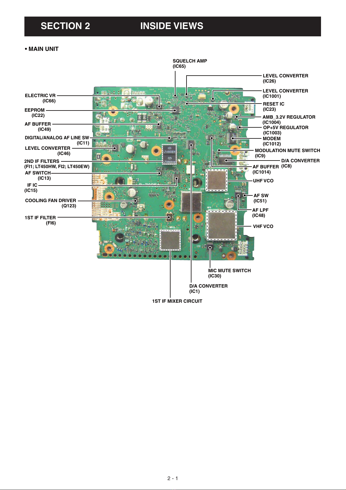
SECTION 4.CIRCUIT DESCRIPTION
LPF
HPF
BPF
RF
AM P
LPF
TX/RX
SW
BPF
BPF
HPF
RF
AM P
TX/RX
SW
RF
AM P
RX
SW
BPF
BPF
RX
SW
RX
SW
RF
AM P
RF
AM P
RX
SW
BPF
BPF
D59,68,75,77
From VHF TX circuit
From UHF TX circuit
To the 1st IF mixer (Q124)
To the 1st IF mixer (Q125)
<- To the 1st IF mixer (IC64)
D30,53,61,62,177
LIMITER
D78,D79
D41,D44,D60
Q19
Q33
<- 810-999 MHz
Q28
<- 420-550 MHz
<- 230-420 MHz
Q35
VHFLPF
UHFLPF
D16
D13
D12,14,23
D56
D57,58
D45,D51
Q34
D36
D18,D20
D9
<- 118-174 MHz
BPF1,2,3
BPF1,2,3
BPF2,3
BPF2,3
BPF1
BPF1
4-1 RECEIVE CIRCUITS
RF CIRCUITS
144 MHz BAND (118–174 MHz)
The RX signals (118–174 MHz) from the antenna are
passed through two LPFs and TX/RX SW for VHF band (D59,
68, 75, 77), and applied to the RF circuit.
The RX signals are passed through the limiter (D78, 79) and
BPF, and amplified by the RF AMP (Q33). The amplified RX
signals are filtered by tuned BPF (D41, 44, 60) to remove
unwanted signals, then applied to the 1st mixer (Q124).
The passband frequency of the tuned BPF (D41, 44, 60) is
tuned by the tuning voltage from the D/A converter controlled
by the CPU (IC25).
300 MHz BAND (230–420 MHz)
The RX signals (230–420 MHz) from the antenna are
passed through the LPF, HPF and TX/RX SW for UHF band
(D30, 53, 61, 62, 177), and applied to the RF circuit.
The RX signals are passed through the RX SW (D56) and
filtered by the tuned BPF (D57, 58) to remove unwanted
signals, then applied to the RF AMP (Q35).
The amplified RX signals are filtered by another tuned BPF
(D45, 51) to remove unwanted signals, and amplified by
another RF AMP (Q34). The RF AMP (Q34) improves the
isolation between the 1st mixer (IC64) and the tuned BPF.
The amplified RX signals are applied to the 1st mixer (IC64).
The pass-band frequencies of the tuned BPFs (D57, 58:
D45, 51) are tuned by the tuning voltage from the D/A
converter controlled by the CPU (IC25).
440 MHz BAND (420–550 MHz)
The RX signals (420–550 MHz) from the antenna are
passed through the LPF, HPF and TX/RX SW for UHF band
(D30, 53, 61, 62, 177), and applied to the RF circuit.
The RX signals are passed through the RX SW (D16) and
tuned BPF (D13) to remove unwanted signals, and applied
to the RF AMP (Q19). The amplified RX signals are filtered
by another tuned BPF (D12, 14, 23) to remove unwanted
signals, then applied to the 1st mixer (Q125).
The pass-band frequencies of tuned BPFs (D13: D12,
14, 23) are controlled by the tuning voltage from the D/A
converter controlled by the CPU (IC25).
800 M Hz BAND (810–999 MHz)
The RX signals (810–999 MHz) from the antenna are
passed through the HPF, and applied to the RF AMP (Q28).
The amplified RX signals are filtered by the tuned BPF (D18,
20) to remove unwanted signals, then applied to the 1st
mixer (IC64) via the RX SW (D9).
The pass-band frequency of tuned BPF (D18, 20) is tuned
by the tuning voltage from the D/A converter controlled by
the CPU (IC25).

4 - 2
• 2ND IF CIRCUITS
X3
BPF
CERAMIC
X2
PLL
IC BPF
CERAMIC
Q52
IC14 FI2
WIDE/NARROW
SELECTOR
IC15
IF IC
(For narrow)
450 kHz 2nd IF filter
(For wide)
FI1
DETECT
SIGNAL
SELECTOR
TCXO
15.3 MHz
X5
IC13
2nd LO
Pin 11(FM/DV mode)
Pin 14(AM mode)
45.9 MHz
From the 1st IF circuits
To the AF filter circuits
(FM/AM mode)
To the digital demodulator circuits
(DV mode)
IF
AM P BPF
XTAL
140_LO
440_LO
UHF_L O
Q66
46.35MHz
FI6
From the 140 MHz band
RF circuit
From the 440 MHz band
RF circuit
To the 2nd IF
circuits
From the 300 MHz and
800 MHz bands RF circuit
D88
LIMIT
Q124
Q125
LIMIT
D1009
IC64
2nd IF AND DEMODULATOR (for FM and AM) CIRCUITS
The 1st IF signal from the 1st IF circuits is applied to the
IF IC (IC15, pin 20). IC15 contains 2nd mixer, limiter AMP,
noise AMP, quadrature detector, RSSI circuit and AM
detector in its package.
The applied 1st IF signal is converted into the 450 kHz 2nd
IF signal by being mixed with tripled reference frequency
signal (45.9 MHz) from the PLL IC (IC14) via the tripler (Q52).
The converted 2nd IF signal is output from pin 3, and passed
through the ceramic filter (FI1 for FM narrow and AM modes,
FI2 for FM and DV modes) to remove sideband noise, then
applied to the IF IC (from pin 7; FM/DV mode/ from pin 5; AM
mode) again.
1st IF CIRCUITS
144 MHz BAND (118–174 MHz)
The RX signals (118–174 MHz) from the RF circuit are
applied to the G1 terminal of Q124 (1st IF mixer), and the
1st LO signals "140_LO" are applied to the G2 terminal of it.
These input signals are mixed to be converted into the
46.350 MHz 1st IF signal.
300 MHz (230–420 MHz) AND 800 MHz (810–999 MHz) BANDS
The RX signals (230–420 MHz and 810–999 MHz) from the
RF circuit are applied to the RX input terminal of IC64 (1st IF
mixer), and the 1st LO signals "UHF_LO" are applied to the
LO input terminal of it.
These input signals are mixed to be converted into the
46.350 MHz 1st IF signal.
440MHz BAND (420–550MHz)
The RX signals (420–550MHz) from the RF circuit are
applied to the G1 terminal of Q125 (1st IF mixer), and the
1st LO signals "440_LO" are applied to the G2 terminal of it.
These input signals are mixed to be converted into the
46.350 MHz 1st IF signal.
The 1st IF signal converted by the 1st mixer is passed
through the 1st IF filter (FI6) to remove unwanted signals.
FI6 is a 4-pole crystal filter contains two filters, and has
adequate selectivity to extract wanted signal.
The filtered 1st IF signal is applied to the 1st IF AMP (Q66)
via the limiter (D1009), and the amplified 1st IF signal is
applied to the IF IC (IC15) via another limiter (D88).
• 1ST IF CIRCUITS

• DIGITAL (DV) DEMODULATOR CIRCUITS
• AF FILTER CIRCUITS AND AF POWER AMPLIFIER
4 - 3
BUFF BUFF
IC49b
To the AF filter circuits
(DV mode)
From the FM demodulator
circuits (DV mode)
CNV. CODEC
LEVEL
IC1014
LINEAR
IC1013
IC1006
MODEM
IC1012
CODEC
DSP
IC1000,1001,1002 AF
AM P
SP1
Internal speaker
J8
[EXTERNAL SPEAKER JACK]
Volume
control
IC38 Q102 IC66
MUTE
SP
SELECT
DIGI/AN
AF
FILTER
AF
FILTER
IC11Q47IC49a
From the FM/AM demodulator circuits
(FM/AM mode)
From the digital demodulator circuits
(DV mode)
AF_VOL_DATA
AF_VOL_CK
AFFIL_SEL
FM DEMODULATOR CIRCUITS
In the FM mode, the filtered 2nd IF signal input from
pin 7 is amplified by the internal limiter amplifier, and FM-
demodulated at the internal quadrature detector. The
demodulated AF signals are then output from pin 11 and
applied to the AF circuits via the AF switch (IC13).
AM DEMODULATOR CIRCUITS
In the AM mode, the filtered 2nd IF signal input from
pin 5 is amplified by the internal limiter amplifier, and AM-
demodulated at the internal AM detector. The demodulated
AF signals are output from pin 14 and applied to the AF filter
circuits via the AF switch (IC13).
DIGITAL (DV) DEMODULATOR CIRCUITS
In the DV mode, the filtered 2nd IF signal input from
pin 7 is amplified by the internal limiter amplifier, and
FM-demodulated at the internal quadrature detector.
The demodulated AF signals are applied to the digital
demodulator circuits via the AF switch (IC13).
The FM-demodulated AF signals from the AF switch (IC13)
are applied to the modem (IC1012) via the two buffers (IC49b;
pins 6, 7 and IC1014), and converted into the digital signal.
The converted digital signal is applied to the DSP CODEC
(IC1) via the level converter (IC1000, 1001, 1002), to be
decoded into the AMBE signal. The decoded AMBE signal is
then applied to the liner CODEC IC (IC1006) to be converted
into the analog audio signal. The converted AF signals are
applied to the RX AF circuits.
AF FILTER CIRCUITS
The demodulated AF signals are applied to the AF filter
(Q47) via the digital/analog signal selector (IC11), to obtain
suitable audio response the for receive mode (FM, AM or
DV).
The frequency response of the filter is controlled by “AFFIL_
SEL” signal from the CPU (IC25).
The filtered AF signals are applied to the variable pass-band
frequency audio filter circuit (IC49a; pins 3, 1). The circuit
reduces audible noises included in the demodulated AF
signals.
The filtered AF signals are applied to the electric volume IC
(IC66) which adjusts the loudness by “AF_VOL_DATA” and
“AF_VOL_CK” signals from the CPU (IC25).
The level-adjusted AF signals are applied to the AF power
AMP (IC38) via the AF mute SW (Q102).
AF POWER AMPLIFIER
The AF signals from the AF mute SW (Q102) are applied to
the AF power AMP (IC38), and amplified to obtain AF output
power. The power-amplified AF signals are applied to the
internal speaker (CHASSIS; SP1) via J8.
If an external speaker is connected to the external speaker
jack (J8), the power-amplified AF signals from the AF power
AMP (IC38) are applied to the connected speaker via J8.

4 - 4
LO
AMP
D/A
BUFF
BUFF
AMP
VCO
SW
VCO
SW
MUTE
Q109
Q111
D145-148
Q73
D87,91,92
Q76
From the TX AF
circuits (FM mode)
From the digital converter
circuits (DV mode)
IC48c
MOD
MOD
MOD
MUTE
Q64
MUTE
IC9
IC8
IC45
To the TX amplifer
circuits
D102
Q113
D160,D175
VHF VCO
UHF VCO
Digi/Ana
line SW
IC34
From the TX AF
circuits
To the modulation circuits
BUFF CNV.
CODEC LEVEL
IC1014
BUFF
IC1015
LINEAR
IC1012
IC1006
MODEM
IC1013
CODEC
DSP
IC1000,1001,1002
MIC
MUT E
Pre-emphasis
and IDC
SPLATTER
MIC
AM P
J2
1
2
3
4
5
6
7
8
ALC
AM P
HPF
MIC
IC48d
SW
MIC GAIN
SWITCH
DA_SEL
AF
IC51
IC32
AF
SW
IC28 IC30
AF
IC29 IC52
SW
Q88 IC48b
Q87
From the microphone
To the modulation circuits
(FM mode)
To the digital converter circuits
(DV mode)
Level
ADJ.
IC48a
4-2 TRANSMITTER CIRCUITS
TX AF CIRCUITS
MIC signals from the connected microphone are passed
through the HPF (Q87), and amplified by the MIC AMP
(IC28). The amplified MIC signals are passed through the
MIC gain SW (Q88) which selects the MIC sensitivity from
“High” or “Low,” and the MIC mute SW (IC30), then passed
through or bypassed the ALC AMP (IC32) via the AF SWs
(IC29 and IC52).
In the DV mode, the MIC signals are applied to the ALC
AMP (IC32) which automatically adjusts the level of MIC
signals for digital processing,
The MIC signals from the AF SW (IC52) are passed through
the pre-emphasis and IDC (for amplitude-limitting) circuits
(IC48b), MIC level adjustment circuit (IC48a) and the
splatter circuit (IC48d) which cuts off the 3 kHz and higher
audio signals. The filtered MIC signals are applied to the
modulation circuits via the AF SW (IC51; pins 1, 7).
In the DV mode, the filtered MIC signals are applied to
the digital converter circuits before being applied to the
modulation circuits via the AF SW (IC51; pins 1, 6).
DIGITAL CONVERTER CIRCUITS
The MIC signals from the TX AF circuits are applied to
the liner CODEC IC (IC1013) via the buffer (IC1014), and
encoded into the digital audio signal. The encoded digital
audio signal is then applied to the DSP CODEC IC (IC1006)
and converted into the AMBE signal. The AMBE signal
is applied to the modem (IC1012) via the level converter
(IC1000, 1001,1002). The modem IC converts the AMBE
signal into the analog signal, and output to the modulation
circuits via the buffer (IC1015) and the digital/analog line SW
(IC34).
MODULATION CIRCUITS
The AF signals from the TX AF circuits (in FM mode) or
digital converter circuits (in DV mode) are applied to the AF
AMP (IC48c). The amplified modulation signals are passed
through the D/A converter (IC8) to be adjusted its level
(=deviation), then applied to the VCO (VHF VCO: Q111,
D145–148/UHF VCO: Q73, D87, 91, 92) via the modulation
mute SWs (IC9, VHF; Q109/UHF; Q64) as the modulation
signals.
The modulated VCO oscillating signal is passed through the
buffer (VHF; Q113/UHF; Q76) and applied to the LO AMP
(IC45) via the VCO SW (VHF; D160, 175/UHF; D102).
The amplified VCO output signals are applied to the TX
amplifier circuits.
• TX AF CIRCUITS
• MODULATION CIRCUITS
• DIGITAL CONVERTER CIRCUITS

• TX AMPLIFIER AND APC CIRCUITS
4 - 5
PWR
DET
LPF
APC
CTRL
HPF
PWR
AM P
ATT
ATTLPF LPF
TX/RX
SW
DRIVE
AMP
HPFLPF
DRIVE
AMP
PWR
DET
LPF
TX/RX
SW
PWR
AM P
DRIVE
PRE
Q25
D59,68,75,77
D42,52,1006
LIMITER
T
LIMITER
D39,D47,D1005
Q22 D25
IC4
D30,53,61,62,177
To UHF RX circuitsTo VHF RX circuits
IC3
Q26
PCON_U PCON_V
D29
IC2
From the frequency synthesizer
circuits
D155
LO SW
LO SW
D103
VHF band TX signal ->
UHF TX signal ->
TX AMPLIFIER CIRCUITS (VHF BAND)
The output signal of VHF VCO (Q111, D145–148) is passed
through the LO SW (D155), LPF and ATT, then applied to
the drive AMP (Q25) via the limiter (D29), to obtain adequate
input level for the power AMP (power MOS-FET module;
IC3).
The amplified TX signal is power-amplified to 50 W (approx.;
25 W for [TPE] ver.) of output power (max.) by the power
AMP (IC3).
The power-amplified TX signal is passed through the LPF
which attenuates harmonic components to prescribed level,
then applied to the antenna connector via the power detector
(D39, 47, 1005), TX/RX SW (D59, 68, 75, 77) and two LPFs.
APC CIRCUITS (VHF BAND)
A portion of the TX signal from IC3 is rectified at the power
detector (D39, 47, 1005), and converted into the DC voltage
which is in proportion to the RF power, and applied to the
operational amplifier (IC4, pin 6). IC4 is an APC amplifier for
both of V/UHF bands. The TX power setting voltage “PCON_
V” from the D/A converter (IC1) is applied to the pin 5 as
a reference. IC4 is rolled as a differential amplifier which
outputs voltage in inverse proportion to rectified one.
When the TX power increased, the rectified voltage also
increased, that causes the decrease of output voltage of
differential amplifier. The decrease of output voltage of
differential amplifier causes the drop of the gate voltage of
IC3, Thus the TX power maintained to keep stable level.
TX AMPLIFIERS (UHF BAND)
The output signal of UHF VCO (Q73, D87, 91, 92) is passed
through the LO SW (D103), HPF and ATT, then applied to
the pre-drive AMP (Q22). The amplified TX signal is applied
to the drive AMP (Q26) via the limiter (D25) and amplified to
obtain adequate input level for the power AMP (power MOS-
FET module; IC2).
The amplified TX signal is power-amplified to 50 W (approx.;
25 W for [TPE] ver.) of output power by the power AMP (IC2).
The power-amplified TX signal is passed through the LPF
which attenuates harmonic components to prescribed level,
then applied to the antenna connector via the power detector
(D42, 52, 1006), TX/RX SW (D30, 53, 61, 62, 177), HPF and
LPF.
APC CIRCUITS (UHF BAND)
A portion of the TX signal from IC2 is rectified at the power
detector (D42, 52, 1006), and converted into the DC voltage
which is in proportion to the RF power, and applied to the
operational amplifier (IC4, pin 2). IC4 is an APC amplifier for
both of V/UHF bands. The TX power setting voltage “PCON_
U” from the D/A converter (IC1) is applied to the pin 3 as
a reference. IC4 is rolled as a differential amplifier which
outputs voltage in inverse proportion to rectified one.
When the TX power increased, the rectified voltage also
increased, that causes the decrease of output voltage of
differential amplifier. The decrease of output voltage of
differential amplifi er causes the drop of the gate voltage of
IC2, Thus the TX power maintained to keep stable level.

4 - 6
X3
(HPF)
LO
AMP
LPF
PLL
IC
LPF
LPF
X2
FIL
LOOP
BUFF
BUFF
VCO
SW
VCO
SW
FIL
LOOP
ATT
LPFATT
ATT
BUFF
ATT
-> RX LO signals for 300 MHz band (230-420 MHz) ->
-> RX LO signals for 800MHz band (810-999 MHz) ->
-> RX LO signals for 440 MHz band (420-550 MHz) ->
-> RX LO signals for 140 MHz band (118-174 MHz) ->
140 MHz band
1st IF MIXER
440 MHz band
1st IF MIXER
800 MHz and
300 MHz bands
1st IF MIXER
Q110,111
D145-148
Q73
D87,91,92
Q52
Q76
Q61,62
IC14
IC15
IF IC
TCXO
15.3MHz
PLLSTB
PLLDATA
PLLCK
X5
45.9 MHz
RF
SW
Q79
IC45
D155
LO SW
D102
D101
LO SW
LO SW
D103
LO SW
LO SW
D170
D104
Q124
To VHF TX Aamplifier
To UHF TX Aamplifier
LO SW
D179
LO SW
D181
D180
Q125
Q113 D160,D175
Q 1015
LO SW
VHF VCO
UHF VCO
IC64
SELECT
VCO
IC1018
4-3 FREQUENCY SYNTHESIZER
VCOs
VHF VCO
The VHF VCO is composed by the oscillator circuit (Q111,
D145, 146, 147) and buffer AMP (Q113), and generates
both of 1st LO signals and TX signal for VHF band.
The VCO oscillating signals are buffer-amplified by Q113,
amplified by the LO AMP (IC45) to obtain adequate LO level,
then applied to the TX amplifiers or 1st IF mixer via the LO
SW, ATT and filter.
While transmitting;
The VCO output signals from the LO AMP (IC45) are applied
to the TX amplifiers via the LO SW (D155) as the TX signal.
While receiving;
The VCO output signals from the LO AMP (IC45) are passed
through the LO SW (D170), ATT and the LPF, then applied to
the 1st IF mixer (Q124), as the 1st LO signals for 140 MHz
band.
The VCO output signals from the LO AMP (IC45) are passed
through the LO SW (D104), ATT, RF SW and LPF, then
applied to the 1st IF mixer (Q125), as the 1st LO signals for
300 MHz band.
UHF VCO
The UHF VCO is composed by the oscillator circuit (Q73,
D87, 91, 92) and buffer AMP (Q76), and generates both of
1st LO signals and TX signal for UHF band.
The VCO oscillating signals are buffer-amplified by Q76,
amplified by the LO AMP (IC45) to obtain adequate LO level,
then applied to the TX amplifiers or 1st IF mixer via the LO
SW, ATT and filter.
While transmitting;
The VCO output signals from the LO AMP (IC45) are applied
to the TX amplifiers via the LO SW (D103) as the TX signal.
While receiving;
The VCO output signals from the LO AMP (IC45) are passed
through the LO SW (D101), ATT, doubler (HPF) and LPF,
then applied to the 1st IF mixer (IC64), as the 1st LO signals
for 800 MHz band.
The VCO output signals from the LO AMP (IC45) are passed
through the LO SW (D179), ATT and the LPF, then applied to
the 1st IF mixer (IC64), as the 1st LO signals for 440 MHz band.
PLL
The PLL circuit provides stable oscillation of the transmit
frequency and receive 1st LO frequency. The PLL output
frequency is controlled by control signals including divide
ratio (“PLLCK,”"PLLDATA”and "PLLSTB") from the CPU
(IC25).
PLL (VHF VCO)
A portion of VHF VCO output signals from the buffer
(Q113) are applied to the PLL IC (IC14) via the VCO switch
(D175). The applied signals are divided at the prescaler and
programmable counter.
The divided signal is phase-compared with the 15.3 MHz
reference frequency signal from the reference frequency
oscillator (X5), at the phase detector.
The phase difference is output from pin 5 as a pulse type
signal after being passed through the internal charge pump.
The output signal is converted into the DC voltage (lock
voltage) by passing through the loop filter (R694-698, C759-
763). The lock voltage is applied to the variable capacitors
(D145, 146), and locked to keep the VCO frequency
constant.
PLL (UHF VCO)
A portion of VHF VCO output signals from the buffer (Q76)
are applied to the PLL IC (IC14) via the VCO switch (Q1015).
The applied signals are divided at the prescaler and
programmable counter.
The divided signal is phase-compared with the 15.3 MHz
reference frequency signal from the reference frequency
oscillator (X5), at the phase detector.
The phase difference is output from pins 15 and 16, and
passed through the external charge pump (Q61, 62) to be
converted into the pulse type signal.
The output signal is converted into the DC voltage (lock
voltage) by passing through the loop filter (R355, 362, 365,
369, 378, C451, 456, 473). The lock voltage is applied to the
variable capacitors (D91, 92), and locked to keep the VCO
frequency constant.
• FREQUENCY SYNTHESIZER CIRCUITS

4 - 7
4-4 CPU (MAIN UNIT; IC25) PORT ALLOCATION
PIN
No.
LINE NAME
DESCRIPTION I/O
3
AN
Audio response select signal.
"H"=FM mode.
"L"=DV mode.
O
4
DA_SEL
Cut-off frequency shifting signal to the
HPF (IC48). O
5
MM_MUTE
MIC mute signal to the MIC mute switch
(IC30).
"H"=MIC mute.
O
6
DCONT
ALC amplifier control signal to the AF
switches (IC29 and IC52).
"H"=ALC amplifier ON.
O
8
1200_
9600SEL
Baud rate select signal to the packet
modulation select switch (IC30). O
9
P_PTT
Packet PTT detect signal. I
10
P_SQL
Packet squelch control signal. O
11
MIC_SENC
Microphone sensitivity select signal.
"H"=High sensitivity. O
16
DADJSEL
Modulation mute signal to the digital
modulation switch (IC34).
17
MOD_DA
Modulation line switching signal to the
MOD mute switches (IC9 and IC67).
"H"=Modulation enable.
O
22
PLLSTB
Strobe signal to the PLL IC ( IC14). O
23
AMC
AM-demodulator circuit control signal.
"L"=While receiving in AM mode (AM-
modulator and AGC circuits are
activated).
O
24
DTCS_SEL
Tone filter switching signal to the
LPF (Q100).
"H"=DTCS mode.
"L"=CTCSS mode.
O
25
R5C
RX circuits control signal.
"H"=RX circuits is activated. O
26
WN_SEL
2nd IF filter (Wide/Narrow) toggling
signal.
"H"=Narrow.
"L"=Wide.
O
28
UTX_C
Transmitting control signal to the UT8 line
regulator (Q13, 17).
"H"=While transmitting in UHF band.
O
29
VCO_SHIFT
VCO oscillating frequency shift signal to
the VHF VCO switch (Q110). O
32
PLLCK
Clock signal to the PLL IC (IC14). O
33
PLLDATA
Data to the PLL IC (IC14). O
34
UNLOCK
PLL unlock signal from the PLL IC ( IC41). I
35
MMUTE
Modulation mute signal to the MOD mute
switch (Q64).
"H"=Modulation muted.
O
36
VTX_C
Transmitting control signal to the VT8 line
regulator (Q12, 15).
"H"=While transmitting in VHF band.
O
37
PLLSW
Lock-up time control signal to the loop
filter.
"H"=Fast lock-up time.
O
38
UVCO_SEL
VCO power control signal to the VCO
select switch (Q65, 68).
"L"=UHF VCO is activated.
O
39
VVCO_SEL
VCO power control signal to the VCO
select switch (Right band VHF; Q65, 68).
"H"=VHF VCO is activated.
O
48
D5VC
Power control signal for the digital
converter circuits. O
52
AFFIL_SEL
Switching signal to the AF filter (Q47).
"H"=FM
"L"=AM/DV
O
55
DTCS
DTCS and CTCS signals. O
PIN
No.
LINE NAME
DESCRIPTION I/O
56
DTMF
Beep, DTMF and european tone (E880
only) signals. O
57
MIC_SEL
Connected microphone detect signal. I
62
MICUD
[UP]/[DWN] key input from connected
microphone (HM-154). I
63
AMRSSI
Inputs RSSI signal (for AM mode) from
the AGC line controller (Q44). I
64
RSSI
While receiving; inputs RSSI signal from
the IF IC (IC15). I
65
IDET
Current level from the current detector
(IC55, D163). I
66
HVin
Divided voltage of the HV line. I
69
WXALT
Demodulated Weather alert signal from
the AF filter. ([USA] only) I
70
DTCS_IN
Demodulated CTCSS and DTCS signals
from the CTCSS filter (Q41). I
71
TEMP
Transceiver's internal temparature from
the thermal detector circuit (R509). I
76
SCL
I/O port for clock signal to the EEPROM
(IC22). I/O
77
AF_VOL_CK
Serial clock signal to the electric volume
IC (IC66). O
78
AF_VOL_
DATA
Data signal to the electric volume IC
(IC66). O
80
PWR
Power control signal to the PWR controller
(Q82).
"H"=While the transceiver power is ON.
O
82
SDA
Data signal to the EEPROM (IC22). I/O
85
MIC_PTT
Input port for [PTT] key on the connected
microphone. I
101
SQL
Noise signal from the IF IC (IC15). I
103
CL_SFT1
Clock frequency shift signal. O
107
ACQ
ACQ signal to the modem IC (IC1012). O
108
98_DATA
Communication signal to the connected
microphone (HM-133). I/O
109
TXDT
TX data (DV) to the modem IC (IC1012). O
110
TXCK
TX clock signal (DV) to the modem IC
(IC1012). O
111
RXDT
RX data (DV) to the modem IC (IC1012). I
112
RXCK
RX clock signal (DV) to the modem IC
(IC1012). I
113
AMBERES
Reset signal to the DSP CODEC (IC1006). O
114
AMBECLK
Clock signal to the DSP CODEC (IC1006). O
115
AMBEEPR
EPR (Encode Packet Ready) signal to the
DSP CODEC (IC1006). O
116
AMBESTB
Strobe signal to the DSP CODEC (IC1006).
O
122
RX_DATA
Data lines for the control unit. I
123
TX_DATA
Data lines for the control unit. O
127
TX232
Data bus for RS-232C communication. O
128
RX232
Data bus for RS-232C communication. I
129
DA_CK
Serial clock signal to the D/A converter. O
130
DA_DATA
Serial data to the D/A converter. O
131
AMBETXD
AMBE RX signal. I
132
AMBETRD
AMBE TX signal. O
134
DA_STB
Strobe signal to the D/A converter. O
142
MOD_MUTE
Packet modulation mute signal. O
143
FIL1(143pin)
AF filter circuits control signals. O
144
FIL2(144Pin)

4 - 8
4-5 VOLTAGE BLOCK DIAGRAM
Voltage from the power supply is routed to the whole of the transceiver via regulators and switches.
PWR
CTRL
+8
REG
IC21
Q81
PWR
CPU5V
NOISE
FIL
FILTER
NOISE
CURRENT
DETECT
IDET
HV HV
TX power
amplifiers (IC2, IC3)
MAIN UNIT CONTROL UNIT
CPU (IC25)
(for current monitoring)
CPU (IC25),
EEPROM (IC22),
Reset IC (IC23), etc.
PLL IC (IC14),
D/A converter (IC8),
ALC IC (IC32), etc.
VCC
5VS
L5V
8V
IC24
D119
Q83,
Q84,
D120
IC55,
5VS
REG
REG
5VS
5V
5V
REG
D164
Q82
VCC
REG
DTMF decoder (IC56),
Electric volume (IC33),
AF mixer (IC59), etc.
Limitter (D165−D168), etc.
AF filter (Q47, Q50),
MIC amplifier (IC28),
APC controller (IC4), etc.
AF power amplifier (IC38)
IC3
+3
REG
CPU (IC13),
Regulator (Q14, Q15),
Protector/Buffer (IC12), etc.
Reset IC (IC9),
LCD module, etc.
5V
+5
REG
+3.2V

¤ REQUIRED INSTRUMENTS
INSTRUMENTS SPECIFIDATION INSTRUMENTS SPECIFIDATION
DC Cable (Supplied with transceiver) JIG cable
(See the illust below)
Power Supply
Output voltages : 13.8 V DC
and 12.0 V DC
Current capacity : More than 15 A
Multimeter Input impedance : 50 kΩ
Measuring range : 0.1–20V/0.01–5 A
RF Power Meter
(terminated type)
Measuring range : 0.1–60 W
Except [TPE]
0.1–30 W [TPE]
Frequency range : 100–600 MHz
Impedance : 50
Ω
SWR : Less than 1.2 : 1
Standard Signal
Generator (SSG)
Frequency range : 0.1–1200 MHz
Output level : 0.04 µV to 32 mV
(–28 dBu to 90 dBu)
Terminator Impedance : 50
Ω
Frequency counter
Frequency range : 0.1–600 MHz
Frequency accuracy :
±0.1 ppm or better
Input level : Less than 1 mW
AC Millivoltmeter Measuring range : 10 mV to 10 V
Attenuator Power attenuation : 40 dB
Capacity : More than 100 W
Modulation
Analyzer
Frequency range : 30–600 MHz
Measuring range : 0 to ±10 kHz Audio generator Frequency range : 300–3000 Hz
Output level : 1–500 mV
MJIG CABLE
8-pin modular jack
q
iuytrew
q
w
e
r
t
y
u
i
8V
MICU/D
EXTMIC
PTT
MICE
MIC
GND
MICIN
y(MIC)
w(MICU/D)
u(GND)
r(PTT)
u(GND)
t(MICE)
AUDIO GENERATOR
(300–3000 Hz/1–500 mV)
+−
22 kΩ
+−
AC MILLIVOLTMETER
(10 mV to 10 V)
PTT
To [ MICROPHONE CONNECTOR]
SECTION 5.ADJUSTMENT PROCEDURE
5 - 1
5-1 PREPARATION

5 - 2
(See the page 5-1)
JIG CABLE
Modulation analyzer
(DC measurable)
Attenuator
40 dB or 50 dB
to the antenna connector
to DC cable
[ANT]
[DC13.8V]
Standard signal generator
–127 to –17 dBm
(0.1 V to 32 mV)
CAUTION:
DO NOT transmit while
SSG is connected to
the antenna connector.
RF power meter
60 W Except [TPE]
30 W [TPE]
DC power supply
13.8 V / 15 A
(For “CURRENT PROTECT
REFERENCE”)
Frequency
counter
to DC cable
DC power supply
12.0 V / 15 A
Oscilloscope
Terminator
(50 Ω)
To [ MICROPHONE CONNECTOR]
MENTERING ADJUSTMENT MODE
qTurn the transceiver power OFF.
wConnect
JIG cable
(See the page 5-1)
to the [MICROPHONE CONNECTOR].
ePush and hold [MONI] and [BAND], turn the transceiver power ON.
Entering adjustment mode, the function display shows the adjustment item and conditions as below.
MQUITTING ADJUSTMENT MODE
• Disconnect the JIG cable, then turn the transceiver power OFF.
MCONNECTION
VFO/MHz
BAND
MODE
VOL
SQL
M/CALL CSDR LOW
MONI
S
.
M
W
M
W
M
E
N
U
Adjustment frequency, mode and TX power
Selects next adjustment item.
Selects previous adjustment item.
<Rotating>
Adjusts the value for the item manually. Connects the JIG cable
(See the page 5-1)
Adjustment item
<Pushing>
• Store the set value.
• Adjusts the value for
the item automatically.
ATTENTION: NEVER change the value of the
adjustment items that are not described in this
ADJUSTMENT PROCEDURES. Otherwise, the
transceiver may not work properly.

5-2 FREQUENCY AND TRANSMIT AMPLIFIER ADJUSTMENT
Select an adjustment item using [VFO/MHz] / [M/CALL], then set the adjustment value as specified using [DIAL].
ADJUSTMENT
ADJUSTMENT
ITEM OPERATION VALUE
REFERENCE
FREQUENCY
[REF]
1 1) Connect an RF power meter to the antenna connector.
2) Loose couple a frequency counter to the antenna
connector.
3) While transmitting, adjust the TX frequency using [DIAL],
then push [BAND] to store the adjustment value.
435.0000 MHz1)
440.0000 MHz2)
VHF BAND
TRANSMIT POWER
[PHL]
1•Connect an RF power meter to the antenna connector. –
[Hi power]
(BAND LOW)
2•While transmitting, adjust the TX power using [DIAL], then
push [BAND] to store the adjustment value.
50 W
(Except [TPE])
25 W ([TPE])
(BAND HIGH) [PHH]
[Mid power]
(BAND LOW) [PML] 3
15 W
(BAND HIGH) [PMH]
[Low power]
(BAND LOW) [PLL] 4
5 W
(BAND HIGH) [PLH]
VHF BAND
CURRENT PROTECT
REFERENCE
[PHL]
1 1) Set the power supply voltage to 12.0 V.
2) Connect an RF power meter to the antenna connector. –
[BAND LOW] 2•While transmitting, push [BAND] to store the adjustment
value.
(Automatic
adjustment)
[BAND HIGH] [PHH] 3
UHF BAND
TRANSMIT POWER [PHL]
1•Connect an RF power meter to the antenna connector. –
[Hi power]
(BAND LOW)
2•While transmitting, adjust the TX power using [DIAL], then
push [BAND] to store the adjustment value.
50 W
(Except [TPE])
25 W ([TPE])
(BAND HIGH) [PHH]
[Mid power]
(BAND LOW) [PML] 3
15 W
(BAND HIGH]) [PMH]
[Low power]
(BAND LOW) [PLL] 4
5 W
(BAND HIGH) [PLH]
UHF BAND
CURRENT PROTECT
REFERENCE
[PHL]
1 1) Set the power supply voltage to 12.0 V.
2) Connect an RF power meter to the antenna connector. –
(BAND LOW) 2•While transmitting, push [BAND] to store the adjustment
value.
(Automatic
adjustment)
(BAND HIGH) [PHH] 3
1)Except [USA], [AUS], [CHN], [EXP]
2)[USA], [AUS], [CHN], [EXP]
5 - 3

5 - 4
5-3 ANALOG DEVIATION ADJUSTMENTS (VHF BAND)
Select an adjustment item using [VFO/MHz] / [M/CALL], then set the adjustment value as specified using [DIAL].
ADJUSTMENT
ADJUSTMENT
ITEM
OPERATION VALUE
VHF BAND
FM DEVIATION
[FMS]
1 1) Connect a modulation analyzer to the antenna connector
through an attenuator, and set is as;
HPF : OFF
LPF : 20 kHz
De-emphasis : OFF
Detector : (P-P)/2
2) Connect an audio generator and an AC millivoltmeter to
the JIG cable
(See the page 5-1)
.
–
[BAND LOW] (FM) 2 1) Set the audio generator as;
Frequency : 1 kHz
Level : 80 mVrms [USA]
: 20 mVrms Except [USA]
2) While transmitting, adjust the deviation using [DIAL], then
push [BAND] to store the adjustment value.
±4.2 kHz
[BAND LOW] (FMN) 3 ±2.1 kHz
[BAND HIGH] (FM)
4 ±4.2 kHz
[BAND HIGH] (FMN) 5±2.1 kHz
VHF BAND
MODULATION
BALANCE
[FMB]
1 1) No audio signals are applied.
2) Connect an oscilloscope to the modulation analyzer. –
[BAND LOW] (FM) 2•While transmitting, adjust the waveform using [DIAL], then
push [BAND] to store the adjustment value.
Set to square
waves
[BAND LOW] (FMN) 3
[BAND HIGH] (FM)
4
[BAND HIGH] (FMN) 5
DTCS DEVIATION
[MDT]
1 1) Connect a modulation analyzer to the antenna connector
through an attenuator, and set is as;
HPF : OFF
LPF : 20 kHz
De-emphasis : OFF
Detector : (P-P)/2
2) No audio signals are applied.
–
[VHF BAND] (FM) 2•While transmitting, adjust the deviation using [DIAL], then
push [BAND] to store the adjustment value. ±0.80 kHz
[VHF BAND] (FMN) 3•Push [VFO/MHz] to skip this item. –
CTCSS DEVIATION
[MCT]
1 1) Connect a modulation analyzer to the antenna connector
through an attenuator, and set is as;
HPF : OFF
LPF : 20 kHz
De-emphasis : OFF
Detector : (P-P)/2
2) No audio signals are applied.
–
[VHF BAND] (FM) 2•While transmitting, adjust the deviation using [DIAL], then
push [BAND] to store the adjustment value. ±0.75 kHz
[VHF BAND] (FMN) 3•Push [VFO/MHz] to skip this item. –

5-4 ANALOG DEVIATION ADJUSTMENTS (UHF BAND)
Select an adjustment item using [VFO/MHz] / [M/CALL], then set the adjustment value as specified using [DIAL].
ADJUSTMENT
ADJUSTMENT
ITEM
OPERATION VALUE
UHF BAND
FM DEVIATION
[FMS]
1 1) Connect a modulation analyzer to the antenna connector
through an attenuator, and set is as;
HPF : OFF
LPF : 20 kHz
De-emphasis : OFF
Detector : (P-P)/2
2) Connect an audio generator and an AC millivoltmeter to
the JIG cable
(See the page 5-1)
.
–
[BAND LOW] (FM) 2 1) Set the audio generator as;
Frequency : 1 kHz
Level : 80 mVrms [USA]
: 20 mVrms Except [USA]
2) While transmitting, adjust the deviation using [DIAL], then
push [BAND] to store the adjustment value.
±4.2 kHz
[BAND LOW] (FMN) 3 ±2.1 kHz
[BAND HIGH] (FM)
4 ±4.2 kHz
[BAND HIGH] (FMN) 5±2.1 kHz
VHF BAND
MODULATION
BALANCE
[FMB]
1 1) No audio signals are applied.
2) Connect an oscilloscope to the modulation analyzer. –
[BAND LOW] (FM) 2•While transmitting, adjust the waveform using [DIAL], then
push [BAND] to store the adjustment value.
Set to square wave
[BAND LOW] (FMN) 3
[BAND HIGH] (FM)
4
[BAND HIGH] (FMN) 5
DTCS DEVIATION
[MDT]
1 1) Connect a modulation analyzer to the antenna connector
through an attenuator, and set is as;
HPF : OFF
LPF : 20 kHz
De-emphasis : OFF
Detector : (P-P)/2
2) No audio signals are applied.
–
[UHF BAND] (FM) 4•While transmitting, adjust the deviation using [DIAL], then
push [BAND] to store the adjustment value. ±0.80 kHz
[UHF BAND] (FMN) 5•Push [VFO/MHz] to skip this item. –
CTCSS DEVIATION
[MCT]
1 1) Connect a modulation analyzer to the antenna connector
through an attenuator, and set is as;
HPF : OFF
LPF : 20 kHz
De-emphasis : OFF
Detector : (P-P)/2
2) No audio signals are applied.
–
[UHF BAND] (FM) 4•While transmitting, adjust the deviation using [DIAL], then
push [BAND] to store the adjustment value. ±0.75 kHz
[UHF BAND] (FMN) 5•Push [VFO/MHz] to skip this item. –
5 - 5
Other manuals for ID-880H
3
This manual suits for next models
1
Table of contents
Other Icom Transceiver manuals