KS-FX202
1-9
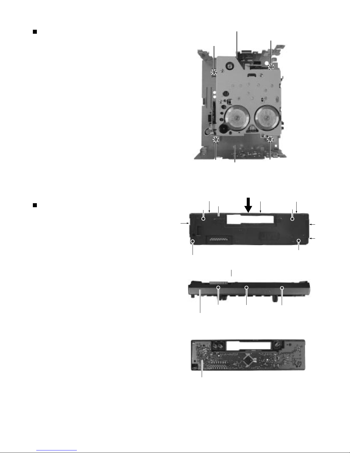
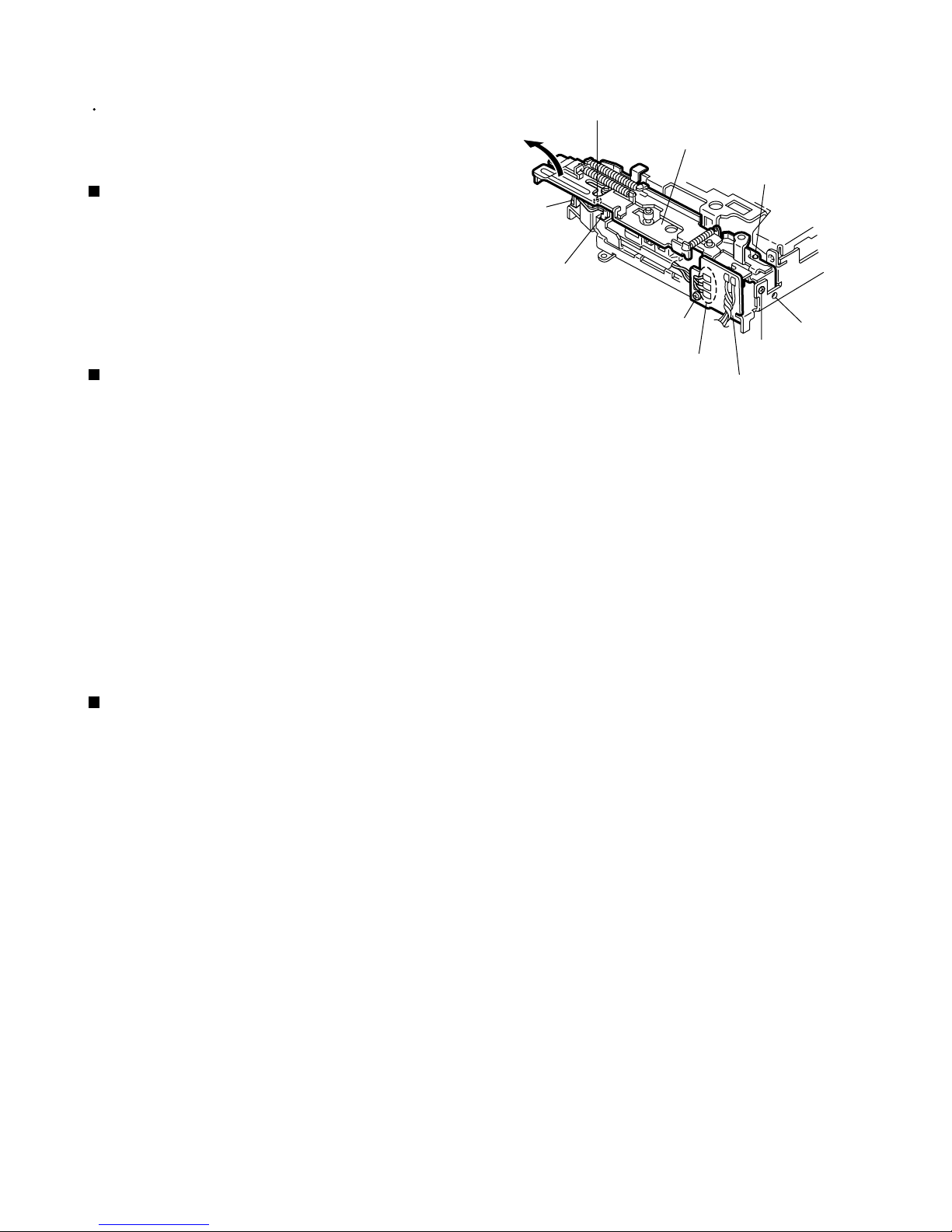
Prior to performing the following procedure, remove
the FF / REW lever assembly.
From the rear of the unit, bend the two tabs f
outwards and disengage the two joints gin the
direction of the arrow.
Push the eject lever and remove the cassette holder
from the playback head. Disengage the two joints h
of the cassette hanger / cassette holder and the eject
lever in the direction of the arrow.
Lift the cassette hanger / cassette holder and disengage
the joint iof the return link and the eject lever.
1.
2.
3.
Removing the cassette hanger / cassette
holder (See Fig.3)
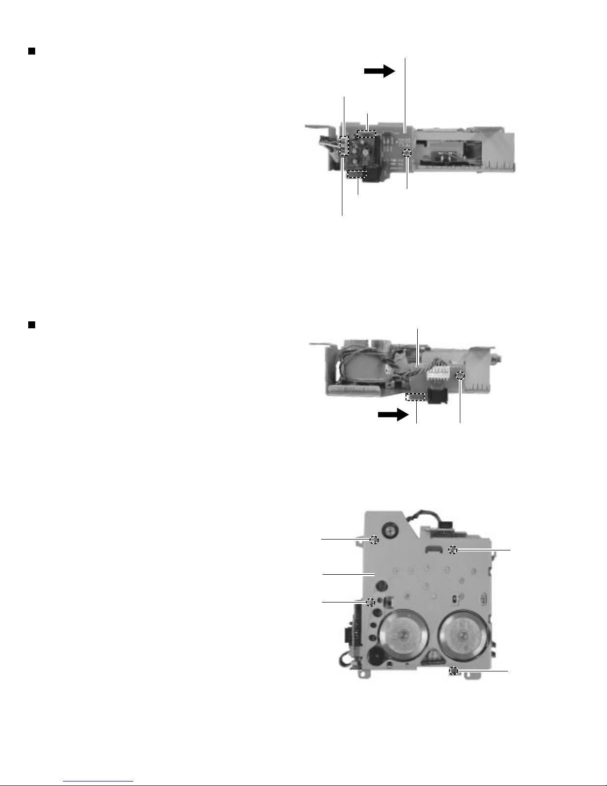
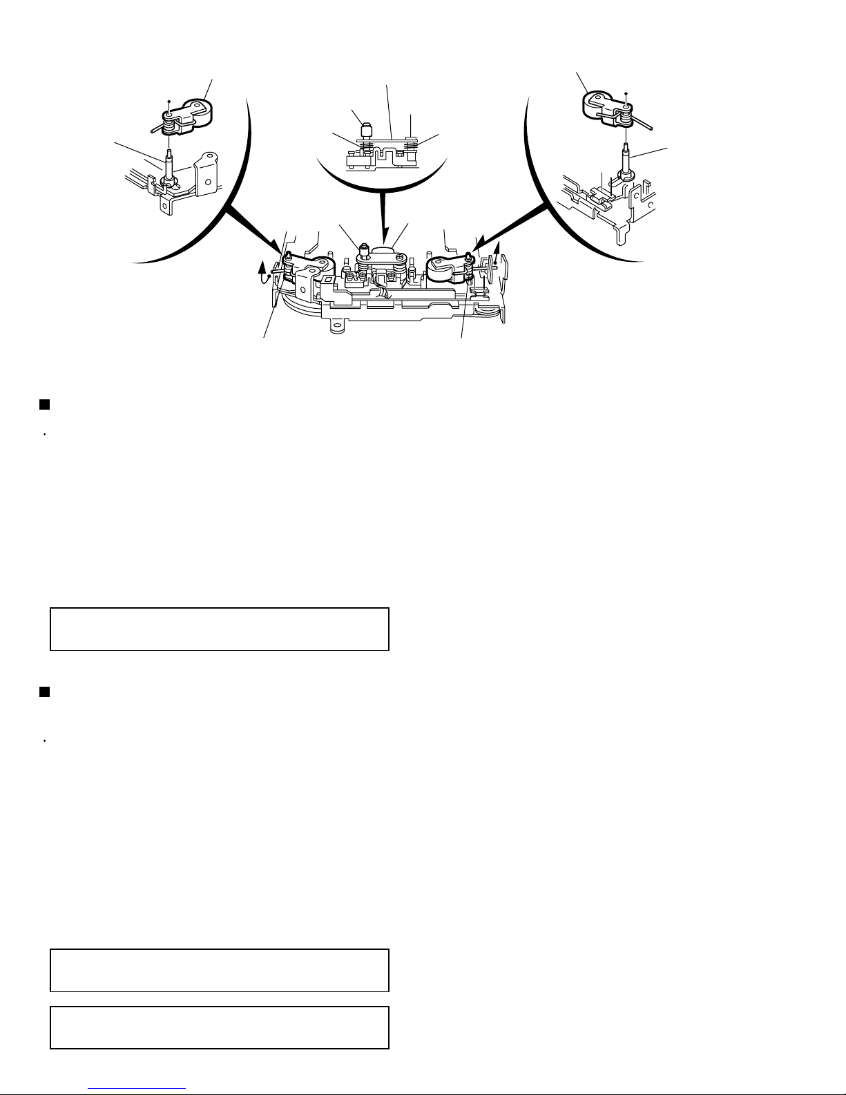
Unsolder the two wires jon the motor assembly.
1.
Turn over the cassette mechanism assembly and
remove the main belt and the sub-belt from the
motor pulley.
2.
Remove the two screws Gattaching the motor
assembly.
3.
Removing the motor assembly
(See Fig.5)
To replace the sub-belt, remove the
main belt and the sub-belt from the
motor pulley. Then remove the three
screws Eand one screw F. Replace
with a new sub-belt while lifting the reel
base assembly slightly.
ATTENTION:
Prior to performing the following procedure, remove
the FF / REW lever assembly and the cassette
hanger / cassette holder.
Remove the C washer and pull out reel disc assembly.
1.
Removing the reel disc assembly
(See Fig.4)
Replace with a new C washer when
reattaching.
ATTENTION:
The main belt can now be removed.
ATTENTION:
Cassette holder
Cassette hanger
Return link
Joint i
Eject lever
Joint h
Joint h
Joint g
Joint g Tab f
Tab f
Reel disc assembly
Flywheel (BF)
Flywheel (BR)
E
E
E
F
G
G
Main-belt
Reel base assembly
Sub-belt
Motor assembly
Motor pulley
Soldering j
Fig.3
Fig.4
Fig.5
C washer
C washer
Chassis