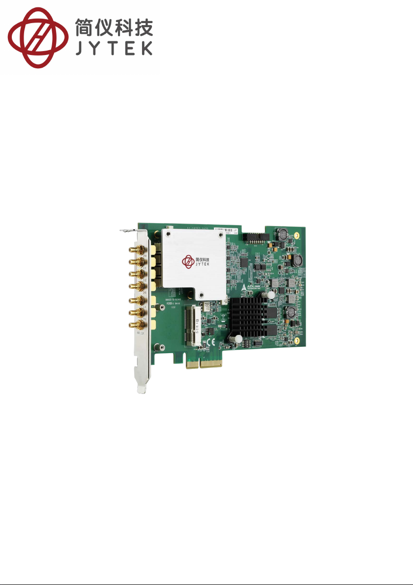
JYTEK PCIe-69834 User manual

PCIe-69834
4CH 16-bit 80MS/s Digitizer
PCIe-69834/PCIe-69834P
User’s Manual
Manual Rev.: 2.00
Revision Date: June 3, 2016
Part No: 50-11263-1000

ii
Revision History
Revision Release Date Description of Change(s)
2.00 June 3. 2016 Initial Release

Preface iii
Preface
Copyright 2016 JYTEK Technology, Inc.
This document contains proprietary information protected by copy-
right. All rights are reserved. No part of this manual may be repro-
duced by any mechanical, electronic, or other means in any form
without prior written permission of the manufacturer.
Disclaimer
The information in this document is subject to change without prior
notice in order to improve reliability, design, and function and does
not represent a commitment on the part of the manufacturer.
In no event will the manufacturer be liable for direct, indirect,
special, incidental, or consequential damages arising out of the
use or inability to use the product or documentation, even if
advised of the possibility of such damages.
Environmental Responsibility
JYTEK is committed to fulfill its social responsibility to global
environmental preservation through compliance with the Euro-
pean Union's Restriction of Hazardous Substances (RoHS) direc-
tive and Waste Electrical and Electronic Equipment (WEEE)
directive. Environmental protection is a top priority for JYTEK.
We have enforced measures to ensure that our products, manu-
facturing processes, components, and raw materials have as little
impact on the environment as possible. When products are at their
end of life, our customers are encouraged to dispose of them in
accordance with the product disposal and/or recovery programs
prescribed by their nation or company.
Conventions
Take note of the following conventions used throughout this
manual to make sure that users perform certain tasks and
instructions properly.
iv Preface
NOTE:
NOTE:
Additional information, aids, and tips that help users perform
tasks.
CAUTION:
Information to prevent minor physical injury, component dam-
age, data loss, and/or program corruption when trying to com-
plete a task.
Information to prevent serious physical injury, component
damage, data loss, and/or program corruption when trying to
complete a specific task.

Table of Contents v
Table of Contents
Preface .................................................................................... iii
List of Figures ....................................................................... vii
List of Tables.......................................................................... ix
1 Introduction ........................................................................ 1
1.1 Features............................................................................... 1
1.2 Applications ......................................................................... 2
1.3 Specifications....................................................................... 2
1.3.1 Analog Input ............................................................... 2
1.3.2 Timebase.................................................................... 4
1.3.3 Triggers ...................................................................... 4
1.3.4 General Specifications................................................ 5
1.4 Software Support ................................................................. 5
1.4.1 WD-DASK................................................................... 6
1.5 Device Layout and I/O Array................................................ 7
2 Getting Started ................................................................. 11
2.1 Installation Environment .................................................... 11
2.2 Installing the Module.......................................................... 12
3 Operations ........................................................................ 13
3.1 Functional Block Diagram.................................................. 13
3.2 Analog Input Channel ........................................................ 13
3.2.1 Analog Input Front-End Configuration ...................... 13
3.2.2 Input Range and Data Format .................................. 14
3.2.3 DMA Data Transfer................................................... 15
3.3 Trigger Source and Trigger Modes.................................... 17
3.3.1 Software Trigger ....................................................... 17

vi Table of Contents
3.3.2 External Digital Trigger ............................................. 17
3.3.3 Analog Trigger .......................................................... 18
3.4 Trigger Modes.................................................................... 18
3.4.1 Post Trigger Mode .................................................... 18
3.4.2 Delayed Trigger Mode .............................................. 19
3.4.3 Pre-Trigger Mode...................................................... 19
3.4.4 Middle Trigger Mode.................................................20
3.4.5 Acquisition with Re-Triggering .................................. 20
3.5 Timebase .............................................................................21
3.5.1 Internal Sampling Clock........................................... 22
3.5.2 External Reference Clock(PCIe-69834P only) .........22
3.6 ADC Timing Control ........................................................... 23
3.6.1 Timebase Architecture.............................................. 23
3.6.2 Basic Acquisition Timing...........................................23
3.7 Synchronizing Multiple Modules ........................................ 25
3.7.2 SSI_TRIG ................................................................. 28
3.8 Multi-boot ........................................................................... 28
3.9 Measurement Function API ............................................... 29
A Appendix: Calibration....................................................... 35
A.1 Calibration Constant .......................................................... 35
A.2 Auto-Calibration ................................................................. 35
Important Safety Instructions.............................................. 39

List of Figures vii
List of Figures
Figure 1-1: Analog Input Channel Bandwidth ............................... 3
Figure 1-2: PCIe-69834 Schematic............................................... 7
Figure 1-3: PCIe-69834 I/O Array ................................................. 8
Figure 3-1: Analog Input Architecture ......................................... 13
Figure 3-2: Linked List of PCI Address DMA Descriptors ........... 16
Figure 3-3: Trigger Architecture .................................................. 17
Figure 3-4: External Digital Trigger ............................................. 18
Figure 3-5: Post-Trigger Acquisition ........................................... 19
Figure 3-6: Delayed Trigger Mode Acquisition............................ 19
Figure 3-7: Pre-Trigger Mode Acquisition ................................... 20
Figure 3-8: Middle Trigger Mode Acquisition .............................. 20
Figure 3-9: Re-Trigger Mode Acquisition .................................... 21
Figure 3-10: PCIe-69834 Clock Architecture ................................ 21
Figure 3-11: Timebase Architecture.............................................. 23
Figure 3-12: Basic Digitizer Acquisition Timing............................. 24
Figure 3-13: Varying Sampling Rates by Adjusting Scan
Interval Counter ........................................................ 24
Figure 3-14: Card Number Configuration Switch .......................... 27
Figure 3-15: Flash Memory Configuration Switch......................... 29
Figure 3-16: Waveform Transition ................................................ 30
Figure A-1: Auto-Calibration Block Diagram ............................... 36
Figure A-2: Auto-Calibration Flow ............................................... 37

viii List of Figures
This page intentionally left blank.

List of Tables ix
List of Tables
Table 1-1: Channel Characteristics................................................... 3
Table 1-2: PCIe-69834 I/O Array Legend ......................................... 9
Table 3-1: Input Range and Data Format ....................................... 14
Table 3-2: Input Range FSR and –FSR Values.............................. 14
Table 3-3: Input Range Midscale Values........................................ 15
Table 3-4: Counter Parameters and Description ............................ 25
Table 3-5: SSI Signal Location and Pin Definition .......................... 26
Table 3-6: Card Number Configuration Settings............................. 28
Table 3-7: Measurement Parameters ............................................. 33

x List of Tables
This page intentionally left blank.

Introduction 1
1 Introduction
The JYTEK PCIe-69834 is a 4-channel, 16-bit, 80MS/s PCI
Express digitizer providing speedy, high quality data acquisition.
Each of the four input channels supports up to 80MS/s sampling,
with16-bit resolution A/D converter. 40MHz bandwidth analog
input with 50Ωimpedance receives ±0.5V, ±1V, ±5V, and ±10V
high speed signals, and a simplified front end and highly stable
onboard reference provide both highly accurate measurement
results and high dynamic performance.
The PCIe-69834, based on x4 lane slot PCI Express
technology, can be used in any standard PCI Express slot, x4, x8,
or x16. With a PCI Express bus interface and extremely large
onboard memory (up to 1GB), the PCIe-69834 easily manages
simultaneous 4-CH data streaming even at the highest sampling
rates.
The PCIe-69834 is auto-calibrated with an onboard reference
cir-cuit calibrating offset and acquiring analog input errors.
Following auto-calibration, the calibration constant is stored in
EEPROM, such that these values can be loaded and used as
needed by the board. There is no requirement to calibrate the
module manually.
1.1 Features
Up to 80MS/s sampling
4 simultaneous analog inputs
High resolution 16-bit ADC
Up to 40 MHz bandwidth for analog input
1GB onboard storage
Programmable input voltage of ±0.5V, ±1V, ±5V, or ±10V
Scatter/gather DMA data transfer for high speed streaming
10 or 20MHz digital onboard filter (FPGA)
PLL module provides precise synch (PCIe-69834P only)
Supports:
One external digital trigger input
One external clock input
Full auto-calibration

2 Introduction
1.2 Applications
Testing/monitoring for Energy Management applications,
including:
Partial discharge
Power line/device monitoring
Non-destructive testing
Radar acquisition
LiDAR
1.3 Specifications
1.3.1 Analog Input
Item Spec Notes
Channels 4 single-ended
Connector
type SMB
Input
coupling DC
ADC
resolution 16-Bit
Input range ±0.5 V, ±1 V, ± 5V, or ± 10V ± 10V only supported
Input impedance 1MΩ
Bandwidth (-
3dB) 40MHz
Overvoltage
±10V sine wave/7Vrms 50Ω, ±0.5V or ±1V or ± 5V
±10V 1MΩ, ±0.5V or ±1V
±30V 1MΩ, ±5V or ±10V
Input
impedance
50Ωor 1MΩ,
software selectable
Digital filter 10MHz or 20MHz,
software selectable
Offset Error
±0.1mV ±0.5V
±0.2mV ±1V
±0.5mV ±5V, or ±10V

Introduction 3
Table 1-1: Channel Characteristics
Figure 1-1: Analog Input Channel Bandwidth
Gain Error ±0.15%
System
Noise (RMS)
0.1mV ±0.5V
0.15mV ±1V
1mV ±5V
1.5 mV ±10 V
Crosstalk -80 dB ±0.5 V
-90 dB ±1 V or ± 5V or ± 10V
SNR 67 dB
THD -78 dB
SFDR 78 dB
Item Spec Notes
-7
-6
-5
-4
-3
-2
-1
0
1
1.00E+05 1.00E+06 1.00E+07 1.00E+08
dB
Frequency (Hz)
CH0 50ȍBandwidth
5V
1V
0.5V

4 Introduction
1.3.2 Timebase
1.3.3 Triggers
Sample Clock Detail Comment
Timebase options
Internal : onboard crystal
oscillator
External : CLK IN (front panel)
Sampling clock
frequency Internal : 80MHz 1.22kS/s to
80MS/s
mpp52±<ycaruccaesabemiT
External reference
clock source
REF_CLK (supported by
PCI-69834P only)
External reference
clock zHM01
External reference
clock input range 3.3V to 5V TTL DC compliant
Trigger Source & Mode
Trigger source Software, external digital trigger, analog trigger, and SSI
(system synchronized interface)
Trigger mode Post trigger, delay trigger, pre-trigger, or middle trigger,
re-trigger for post trigger and delay trigger modes
Digital Trigger Input
Sources Front panel SMB connector
Compatibility 3.3 V TTL, 5 V tolerant
Input high threshold 2.0 V
Input low threshold (VIL) 0.8 V
Maximum input overload -0.5 V to +5.5 V
Trigger polarity Rising or falling edge

Introduction 5
1.3.4 General Specifications
1.4 Software Support
JYTEK provides versatile software drivers and packages to
suit various user approaches to building a system. Aside
from pro-gramming libraries, such as DLLs, for most
Windows-based sys-tems, JYTEK also provides drivers
for other application environments .
Pulse width 20 ns minimum
Specifications
Dimensions 167.64 W x 106.68 H mm (6.53 x 4.16 in)
Bus interface PCI Express Gen 1 x 4
Operating Temperature: 0°C - 50°C
Relative humidity: 5% - 95%, non-condensing
Storage Temperature: -20°C - +80°C
Relative humidity: 5% - 95%, non-condensing
Calibration
Onboard reference +1.8V, +0.9V, and +0.45V
Temperature coefficient 1.0 ppm/°C
Warm-up time 15 minutes
PCIe-69834 PCIe-69834P
Power Rail Standby
Current (mA)
Full Load
(mA)
Standby
Current (mA)
Full Load
(mA)
3.3V 18 18 18.7 21.4
12V 450 470 675 697
Total RMS
Power (W) 5.459 5.699 8.162 8.435
Digital Trigger Input

6 Introduction
All software options are included in the JYTEK All-in-One CD.
Commercial software drivers are protected with licensing codes.
Without the code, you may install and run the demo version for
trial/demonstration purposes for only up to two hours. Contact
your JYTEK dealer to purchase the software license.
1.4.1 WD-DASK
WD-DASK includes device drivers and DLL for Windows XP/7/8/
10. DLL is binary compatible across Windows XP/7/8/10. This
means all applications developed with WD-DASK are compatible
with these Windows operating systems. The development environ-
ment may be VB, VB.NET, VC++, BCB, and Delphi, or any Win-
dows programming language that allows calls to a DLL. The WD-
DASK user and function reference manuals are on the JYTEK
All-in-One CD.

Introduction 7
1.5 Device Layout and I/O Array
Figure 1-2: PCIe-69834 Schematic
The PCIe-69834 I/O array is labeled to indicate connectivity,
as shown.
NOTE:
NOTE:
All dimensions are in mm

8 Introduction
Figure 1-3: PCIe-69834 I/O Array
All I/O connectors are SMB snap-on.

Introduction 9
Table 1-2: PCIe-69834 I/O Array Legend
Input Faceplate
Label Remark
Analog CH0
Analog Input Channel
Analog CH1
Analog CH2
Analog CH3
Ext. Digital
Trigger TRG
External digital trigger input,
receiving trigger signal from
external instrument and initiating
acquisition
Ext. Reference
Clock Input REF_CLK
(PCIe-69834P with PLL module
only)
REF_CLK can be used to receive
an external reference 10MHz clock
to generate ADC timebase. See
Section 3.5.2 External Reference
Clock (PCIe-69834P only)

10 Introduction
This page intentionally left blank.
This manual suits for next models
1
Table of contents
Other JYTEK Measuring Instrument manuals
Popular Measuring Instrument manuals by other brands

Anritsu
Anritsu VectorStar ME7838 4 Series Maintenance manual

Tektronix
Tektronix 6 series Declassification and security instructions

Bosch
Bosch LR40G Operating/safety instructions

Extech Instruments
Extech Instruments MO220 user guide

Hach
Hach TL2300 user manual

Agilent Technologies
Agilent Technologies Seahorse XFe operating manual