Laird AC4868 User manual

Americas : +1-800-492-2320 Option 3
Europe : +44-1628-858-940
Hong Kong : +852-2268-6567 x026
www.lairdtech.com/ramp
AC4868 868 MHz Transceiver
User’s Guide
Version 2.0

AC4868 868 MHz Transceiver
User’s Manual
Americas: +1-800-492-2320 Option 3 2 Laird Technologies
Europe: +44-1628-858-940
Hong Kong: +852 2923 0610
www.lairdtech.com/ramp
REVISION HISTORY
Revision
Date
Description
1.0 29 August 2005 Initial Release Version
1.1 7 October 2005 Added Declaration of Conformity
1.2 29 May 2007 Updated serial interface section.
Corrected EEPROM write command response.
1.3 18 September 2007 Internal Release
1.4 5 September 2008 Updated to Laird Technologies branding. Clarified Duty Cycle
calculations. Updated information on client to client
communications. Corrected Read Temperature Command to a
max of 0x50. Updated Minimum Baud Rate.
2.0 13 November 2013 Updated to new Laird formatting. General edits.

AC4868 868 MHz Transceiver
User’s Manual
Americas: +1-800-492-2320 Option 3 3 Laird Technologies
Europe: +44-1628-858-940
Hong Kong: +852 2923 0610
www.lairdtech.com/ramp
CONTENTS
Revision History............................................................................................................................................ 1
Overview....................................................................................................................................................... 5
Features ........................................................................................................................................................ 5
Networking and Security........................................................................................................................ 5
Easy to Use ............................................................................................................................................ 5
Specifications ............................................................................................................................................... 6
Module Specifications ................................................................................................................................ 6
Electrical Specifications............................................................................................................................... 7
Pin Definitions............................................................................................................................................ 7
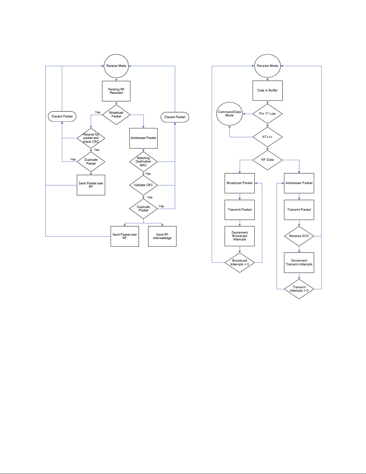
Theory of Operation.................................................................................................................................... 9
RF Architecture........................................................................................................................................... 9
Modes of Operation................................................................................................................................... 9
Transmit Mode ...................................................................................................................................... 9
Receive Mode ........................................................................................................................................ 9
Command Mode ................................................................................................................................... 9
Duty Cycle Limitations ............................................................................................................................... 11
European Regulations .............................................................................................................................. 11
Radio Operation....................................................................................................................................... 11
Transmit Calculations........................................................................................................................... 11
Serial Interface ........................................................................................................................................... 12
Serial Communications............................................................................................................................. 12
Asynchronous Operation ..................................................................................................................... 12
Parity ................................................................................................................................................... 12
OEM Host Data Rate ................................................................................................................................ 13
Serial Interface Baud Rate......................................................................................................................... 13
Interface Timeout / RF Packet Size ............................................................................................................ 13
Flow Control ............................................................................................................................................ 14
Half Duplex / Full Duplex .......................................................................................................................... 14
System Timing and Latency ...................................................................................................................... 15
System Throughput.................................................................................................................................. 15
Software Interface ..................................................................................................................................... 16
Networking .............................................................................................................................................. 16
Range Refresh.......................................................................................................................................... 16
Auto Config Parameters........................................................................................................................... 16
Max Power............................................................................................................................................... 17
Timing Diagrams........................................................................................................................................ 18
AC 4868-250 Timing Diagrams................................................................................................................ 18
Hardware Interface.................................................................................................................................... 20
Pin Definitions.......................................................................................................................................... 20
Generic I/O .......................................................................................................................................... 20
TXD and RXD....................................................................................................................................... 20
Hop Frame........................................................................................................................................... 20
CTS...................................................................................................................................................... 20
GND .................................................................................................................................................... 20
RTS ...................................................................................................................................................... 20
Test / 9600 Baud.................................................................................................................................. 21
UP_Reset ............................................................................................................................................. 21
Command / Data ................................................................................................................................. 21
AD In and DA Out................................................................................................................................ 21
In Range .............................................................................................................................................. 21
Configuring the AC4868-250 .................................................................................................................... 22
AT Commands ......................................................................................................................................... 22

AC4868 868 MHz Transceiver
User’s Manual
Americas: +1-800-492-2320 Option 3 4 Laird Technologies
Europe: +44-1628-858-940
Hong Kong: +852 2923 0610
www.lairdtech.com/ramp
On-the-Fly Control Commands ............................................................................................................ 23
Command Descriptions ............................................................................................................................ 24
Enter AT Command Mode ................................................................................................................... 24
Exit AT Command Mode...................................................................................................................... 24
Status Request ..................................................................................................................................... 24
Change Server / Client ......................................................................................................................... 25
Sleep Walk Power-Down ..................................................................................................................... 25
Sleep Walk Power-Down Wake Up ...................................................................................................... 25
Broadcast Packets ................................................................................................................................ 25
Write Destination Address ................................................................................................................... 26
Read Destination Address .................................................................................................................... 26
Auto Destination.................................................................................................................................. 26
Read Digital Inputs............................................................................................................................... 26
Read ADC............................................................................................................................................ 27
Write Digital Outputs........................................................................................................................... 27
Write DAC ........................................................................................................................................... 27
Set Max Power..................................................................................................................................... 28
Transmit Buffer Empty ......................................................................................................................... 28
Deep Sleep Mode ................................................................................................................................ 28
Read Temperature ............................................................................................................................... 28
EEPROM Byte Read .............................................................................................................................. 28
EEPROM Byte Write ............................................................................................................................. 29
Reset ................................................................................................................................................... 29
EEPROM Parameters .................................................................................................................................. 30
Dimensions ................................................................................................................................................. 33
Mechanical Drawings ............................................................................................................................... 33
Ordering Information................................................................................................................................ 34
Product Part Number Tree ........................................................................................................................ 34
Developer Kit Part Numbers ..................................................................................................................... 34
Compliancy Information............................................................................................................................ 35
Agency Identification Numbers................................................................................................................. 35
Approved Antenna List............................................................................................................................. 35
OEM Equipment Labeling Requirements................................................................................................... 35
Country Restrictions ................................................................................................................................. 36
Country Notification................................................................................................................................. 36
Declaration of Conformity........................................................................................................................ 37
Appendix I: Sample Power Supply............................................................................................................ 38
Bill of Materials ........................................................................................................................................ 38
Schematic ................................................................................................................................................ 39
PCB Layout............................................................................................................................................... 39
Appendix II: 5V to 3.3V Levels .................................................................................................................. 41
Voltage Level Conversion ICs.................................................................................................................... 41
Passive Resistor Voltage Divider ................................................................................................................ 41

AC4868 868 MHz Transceiver
User’s Manual
Americas: +1-800-492-2320 Option 3 5 Laird Technologies
Europe: +44-1628-858-940
Hong Kong: +852 2923 0610
www.lairdtech.com/ramp
OVERVIEW
The compact AC4868-250 868MHz transceiver can replace miles of cable in
harsh industrial environments. Using field-proven technology which needs
no additional CE licensing in Europe, OEMs can easily make existing systems
wireless with little or no RF expertise.
The AC4868-250 is a member of Laird Technologies’s ConnexRF OEM
transceiver family. The AC4868-250 is designed for integration into OEM
systems operating under European ETSI regulations for the 868 - 870 MHz
band.
AC4868-250 transceivers provide an asynchronous TTL/RS-485 level serial
interface for OEM Host communications. Communications include both
system and configuration data. The Host supplies system data for transmission to other Host(s). Configuration
data is stored in the on-board EEPROM. All synchronization and RF system data transmission/reception is
performed by the transceiver.
AC4868-250 transceivers can operate in a Point-to-Point, Point-to-Multipoint, or Peer-to-Peer architecture.
The AC4868-250 utilizes a single channel synchronization allowing all radios to communicate with any radio
in range. Optionally any radio can be configured as a Server to provide a synchronization beacon. This beacon
is used by the Client radios to determine In Range status and for Auto Destination addressing.
This document contains information about the hardware and software interface between a Laird Technologies
AC4868-250 transceiver and an OEM Host. Information includes the theory of operation, specifications,
interface definition, configuration information and mechanical drawings. The OEM is responsible for ensuring
the final product meets all appropriate regulatory agency requirements listed herein before selling any
product.
Note: Unless mentioned specifically by name, the AC4868-250 modules will be referred to as the “radio”
or “transceiver”. Individual naming is used to differentiate product specific features. The host
(PC/Microcontroller/Any device to which the AC4868-250 module is connected) will be referred to
as “OEM Host”.
FEATURES
Networking and Security
Drop-in replacement for AC4490 900
MHz & AC4424 2.4 GHz product
families
Generic I/O digital lines and integrated
DAC/ADC functions
Retries and Acknowledgements
Low latency and high throughput
Easy to Use
Software selectable interface baud rates from 1200 bps
to 57.6 kbps
Low cost, low power and small size ideal for high
volume, portable and battery powered applications
All modules are qualified for Industrial temperatures
(-40°C to 80°C)
Advanced configuration available using AT commands
Server/Client or peer-to-peer communication

AC4868 868 MHz Transceiver
User’s Manual
Americas: +1-800-492-2320 Option 3 6 Laird Technologies
Europe: +44-1628-858-940
Hong Kong: +852 2923 0610
www.lairdtech.com/ramp
SPECIFICATIONS
Module Specifications
Table 1: General Specifications
Parameter
Description
20 Pin Interface Connector Molex 87759-0030, mates with Samtec SMM-110-02-S-D
RF Connector Telegartner J01341C0081, mates with any manufacturer’s MMCX style plug
Antenna AC4868-250: MMCX Connector
Serial Interface Data Rate Baud rates from 1200 bps to 57.6 kbps
Power Consumption
(typical)
10% TX 50% TX 100% TX 100% RX Pwr-Down Deep Sleep
54 mA 138 mA 240 mA 36 mA TBD 24 mA
Channels Single Channel
Security One byte System ID. 56-bit DES encryption key.
Interface Buffer size Input/Output:256 bytes each
Physical Dimensions Transceiver with MMCX Connector: 1.65” x 1.9” x 0.20”
Table 2: Transceiver Specifications
Parameter
Description
Frequency Band Europe 500 mW: 869.4 - 869.65 MHz
RF Data Rate 19.2 kbps or 28.8 kbps dependent on interface baud rate
RF Technology Single Frequency FSK
Output Power Conducted (no antenna) EIRP (2.5 dBi gain antenna)
186 mW typical 250 mW typical
Supply Voltage Pin 10 (uP power): 3.3 – 5.5V ±50mV ripple; draws ~30-50mA. Must be connected.
Pin 11 (PA power): 3.3 ±3%, ±100mV ripple; draws most current. Must be connected.
Sensitivity -103dBm typical @ 28.8kbps RF Data Rate
EEPROM write cycles 20000
Hop period 53 ms
Range, Line of Sight
(2.5dBi gain ant.)
Up to 15 km (9.3 miles)
Table 3: Environmental Specifications
Parameter
Description
Operating Temp -40˚C to +80˚C
Storage Temp -50˚C to +85˚C
Humidity (non-condensing) 10% to 980%

AC4868 868 MHz Transceiver
User’s Manual
Americas: +1-800-492-2320 Option 3 7 Laird Technologies
Europe: +44-1628-858-940
Hong Kong: +852 2923 0610
www.lairdtech.com/ramp
Electrical Specifications
Table 4: Input Voltage Characteristics
Table 5: Output Voltage Characteristics
Signal Name
Module Pin
Type
High Min.
Low Max.
Unit
GO0 1 O 2.5 @ 8mA 0.4 @ 8mA V
TXD 2 O 2.5 @ 2mA 0.4 @ 2mA V
RS485 A/B 2,3 I/O 3.3 @ 1/8 Unit Load N/A V
CTS 7 O 2.5 @ 2mA 0.4 @ 2mA V
GO1 8 O 2.5 @ 2mA 0.4 @ 2mA V
DA_Out 19 O N/A N/A V
In_Range 20 O 2.5 @ 2mA 0.4 @ 2mA V
Pin Definitions
Pin #
Type
Signal Name
Function
1 O GO0 Generic Output pin
2 O TXD Transmitted data out of the transceiver
I/O RS485 A (true) Non-inverted RS-485 representation of serial data
3 I RXD Data input to the transceiver
I/O RS485 B (Invert) Mirror image of RS-485 A
4 I GI0 Generic Input pin
5,16 GND GND Signal Ground
6 N/C This pin has an internal connection and should be left disconnected.
7 O CTS Clear to Send – Active Low when the transceiver is ready to accept data
for transmission.
8 I RTS Request to Send – When enabled in EEPROM, the OEM Host can take
this High when it is not ready to accept data from the transceiver.
Note
: Keeping RTS High for too long can cause data loss.
9 O GO1 Generic Output pin
10 PWR VCC1 3.3 – 5.5V, ±50mV ripple. Powers the radio’s uP. Draws ~30-50mA.
11 PWR VCC2 3.3V, ±50mV ripple. Powers the radio’s power amplifier. Current draw
depends on duty cycle and output power.
Signal Name
High Min.
High Max.
Low Min.
Low Max.
Unit
RS485 A/B N/A 12 -7 N/A V
RXD 2.31 3.3 0 0.99 V
GI0 2.31 3.3 0 0.99 V
RTS 2.31 3.3 0 0.99 V
TEST 2.31 3.3 0 0.99 V
GI1 2.31 3.3 0 0.99 V
UP_Reset 0.8 3.3 0 0.6 V
Command/Data 2.31 3.3 0 0.99 V
AD In N/A 3.3 0 N/A V

AC4868 868 MHz Transceiver
User’s Manual
Americas: +1-800-492-2320 Option 3 8 Laird Technologies
Europe: +44-1628-858-940
Hong Kong: +852 2923 0610
www.lairdtech.com/ramp
12 I Test Test Mode – When pulled logic Low and then applying power or
resetting, the transceiver’s serial interface is forced to a 9600, 8-N-1 rate.
To exit, the transceiver must be reset or power-cycled with Test Mode
logic High.
13 N/C This pin has an internal connection and should be left disconnected.
14 I GI1 Generic Input pin
15 I UP_RESET RESET – Controlled by the AC4868-250 for power-on reset if left
unconnected. After a stable power-on reset, a logic High pulse will reset
the transceiver.
17 I CMD?Data When logic Low, the transceiver interprets OEM Host data as command
data. When logic High, the transceiver interprets OEM Host data as
transmit data.
18 I AD In 10 bit Analog Data Input
19 O DA_Out 10 bit Analog Data Output
20 O In_Range When logic Low, a Client is in range of a Server on same Channel and
System ID. Always low on a Server.

AC4868 868 MHz Transceiver
User’s Manual
Americas: +1-800-492-2320 Option 3 9 Laird Technologies
Europe: +44-1628-858-940
Hong Kong: +852 2923 0610
www.lairdtech.com/ramp
THEORY OF OPERATION
RF Architecture
The AC4868-250 is a single channel radio transceiver. Each unit can be configured as a Server or as a Client.
Servers are responsible for sending out beacons and for allow for radios to be configured very simply in a
point-to-multipoint network. Servers are not required for operation, but if they are used, there should only be
one Server per network. All other radios in the network should be configured as Clients. Clients can
communicate point-to-point or in a mesh with or without a Server.
Modes of Operation
The AC4868-250 has three different operating modes; Receive, Transmit, & Command Mode. If the
transceiver is not communicating with another radio, it will be in Receive Mode actively listening for a beacon
from the Server. If the Client determines that the beacon is from a server operating on the same RF Channel
and System ID, it will respond by asserting In_Range Low. A transceiver will enter Transmit or Command mode
when the OEM Host sends data over the serial interface. The state of the Command/Data pin (Pin 17) or the
data contents determine which of the two modes will be entered.
Transmit Mode
All packets sent over the RF are either Addressed or Broadcast packets. Broadcast and Addressed delivery can
be controlled dynamically with the API Control byte and corresponding on-the-fly commands. To prohibit
transceivers from receiving broadcast packets, Unicast only can be enabled.
Addressed Packets
When sending an addressed packet, the RF packet is sent only to the receiver specified in destination address.
To increase the odds of successful delivery, Transmit retries are utilized. transparent to the OEM Host; the
sending radio will send the RF packet to the intended receiver. If the receiver receives the packet free of errors,
it will return an RF acknowledge within the same 53 ms hop. If a receive acknowledgement is not received, the
radio will use a transmit retry to resend the packet. The radio will continue sending the packet until either (1)
an acknowledgement is received or (2) all transmit retries have been used. The received packet will only be
sent to the OEM Host if and when it is received free of errors.
Broadcast Packets
When sending a broadcast packet, the RF packet is sent out to every eligible transceiver on the network. To
increase the odds of successful delivery, Broadcast attempts are utilized. Transparent to the OEM Host, the
sending radio will send the RF packet to the intended receiver(s). Unlike transmit retries, all broadcast attempts
are used; regardless of when the RF packet is actually received and without RF acknowledgements. If the
packet is received on the first attempt, the receiver will ignore the remaining broadcast attempts. The received
packet will only be sent to the OEM Host if and when it is received free of errors.
Receive Mode
When a transceiver is not in Transmit or Command mode, it will be in Receive Mode listening for data. While
in Receive Mode, subsequent data of up to 80 bytes can be received every hop (53 ms).
Command Mode
A radio will enter Command Mode when data is received over the serial interface from the OEM Host and
either the Command/Data pin (pin 17) is logic Low or the received data contains the “AT+++” (Enter AT

AC4868 868 MHz Transceiver
User’s Manual
Americas: +1-800-492-2320 Option 3 10 Laird Technologies
Europe: +44-1628-858-940
Hong Kong: +852 2923 0610
www.lairdtech.com/ramp
Command Mode) command. Once in Command Mode, all data received by the radio is interpreted as
command data. Command Data can be either EEPROM Configuration or On-The-Fly commands.
Figure 1: Pending RF and Data in Buffer Flow

AC4868 868 MHz Transceiver
User’s Manual
Americas: +1-800-492-2320 Option 3 11 Laird Technologies
Europe: +44-1628-858-940
Hong Kong: +852 2923 0610
www.lairdtech.com/ramp
DUTY CYCLE LIMITATIONS
European Regulations
ETSI requirements as specified in the ETSI EN 300 220-1 define the requirements for the 868-870MHz bands.
For a conducted output of 180mW and radiated outputs up to 500mW, the maximum allowed duty cycle is
<10%. This duty cycle is measured as the amount of TX time on, monitored over one hour and relative to a
one hour period. Thus for the AC4868-250, the maximum “on” time in an hour cannot exceed six minutes.
Radio Operation
The AC4868 will transmit data whenever data is present on the serial UART. Data will be transmitted for
Broadcast packets according to the value of the Broadcast Attempts. For Addressed Packets data will be
transmitted until a successful acknowledgement is received. The OEM is responsible for limiting the
Transmitter’s “on” time to less than the duty cycle regulations.
Transmit Calculations
For a rough estimate the TX Time on is 53ms * the number of retries or attempts. By default this is 212ms. For
servers you need to a 5ms beacon.
The interval time is based on an increment of data equal to or less than the packet size given in Table 6.
Table 6: RF Packet Size
RF Baud Rate
Addressed Mode
RF Packet Size
19200 Addressed 0x24
28800 Addressed 0x50
19200 Broadcast 0x40
28800 Broadcast 0x60
So the total TX On Time is 5ms (For Servers) + Data Size/RF Packet Size * Number of Retries/Attempts.

AC4868 868 MHz Transceiver
User’s Manual
Americas: +1-800-492-2320 Option 3 12 Laird Technologies
Europe: +44-1628-858-940
Hong Kong: +852 2923 0610
www.lairdtech.com/ramp
SERIAL INTERFACE
In order for the OEM Host and a transceiver to communicate over the serial interface they need to have the
same serial data rate. Refer to the following sections to ensure that the OEM Host data rate matches the serial
interface baud rate.
Serial Communications
The AC4868-250 is a TTL device which can be interfaced to a compatible UART (microcontroller) or level
translator to allow connection to serial devices. UART stands for Universal Asynchronous Receiver Transmitter
and its main function is to transmit or receive serial data.
Asynchronous Operation
Since there is no separate clock in asynchronous operation, the receiver needs a method of synchronizing with
the transmitter. This is achieved by having a fixed baud rate and by using START and STOP bits. A typical
asynchronous mode signal is shown below.
Figure 2: Asynchronous Mode Signal
The UART outputs and inputs logic level signals on the TX and RX pins. The signal is high when no data is
being transmitted and goes low when transmission begins.
The signal stays low for the duration of the START bit and is followed by the data bits; LSB first. The STOP bit
follows the last data bit and is always high. After the STOP bit has completed, the START bit of the next
transmission can occur.
Parity
A parity bit is used to provide error checking for a single bit error. When a single bit is used, parity can be
either even or odd. Even parity means that the number of ones in the data and parity sum to an even number
and vice-versa. The ninth data bit can be used as a parity bit if the data format requires eight data bits and a
parity bit as shown below.
Figure 3: Even Parity Bit
Note: Enabling parity cuts throughput and the interface buffer in half.

AC4868 868 MHz Transceiver
User’s Manual
Americas: +1-800-492-2320 Option 3 13 Laird Technologies
Europe: +44-1628-858-940
Hong Kong: +852 2923 0610
www.lairdtech.com/ramp
OEM Host Data Rate
The OEM Host Data Rate is the rate with which the OEM Host and transceiver communicate over the serial
interface. Possible values range from 1200 bps to 57,600 bps.
Note: Enabling Parity cuts throughput in half and the Interface Buffer size in half. Table 7 shows the
supported asynchronous serial data formats.
Table 7: Supported Serial Formats
Data Bits
Parity*
Stop Bits
Transceiver Programming Requirements
8 N 1 Parity Disabled
7 N 2 Parity Disabled
7 E,O,M,S 1 Parity Disabled
9 N 1 Parity Enabled
8 N 2 Parity Enabled
8 E,O,M,S 1 Parity Enabled
7 E,O,M,S 2 Parity Enabled
*Mark (M) corresponds to 1 & Space (S) corresponds to 0
Serial Interface Baud Rate
This two-byte value determines the baud rate used for communicating over the serial interface to a
transceiver. The Table below lists values for some common baud rates. Baud rates below 1200 and above
57600 baud are not supported. For a baud rate to be valid, the calculated baud rate must be within ±3% of
the OEM Host baud rate. If the Test pin (Pin 12) is pulled logic Low at reset, the baud rate is forced to 9600.
Baud
BaudL
(0x42)
BaudH
(0x43)
RF Baud (not
adjustable)
Minimum Interface
Timeout (0x58)
Stop Bit Delay
(0x3F)
57600
1
0xFC 0x00 28800 0x02 0x03
38400 0xFA 0x00 19200 0x02 0x08
28800 0xF8 0x00 28800 0x02 0x0E
19200 0xF4 0x00 19200 0x03 0x19
14400 0xF0 0x00 28800 0x04 0x23
9600 0xE8 0x00 19200 0x05 0x39
1. 57600 is the default baud rate.
Interface Timeout / RF Packet Size
Interface Timeout (EEPROM address 0x58), in conjunction with RF Packet Size (EEPROM address 0x5B),
determines when a buffer of data will be sent out over the RF as a complete RF packet, based on whichever
condition occurs first.
Interface Timeout – Interface Timeout specifies a maximum byte gap between consecutive bytes. When that
byte gap is exceeded, the bytes in the transmit buffer are sent out over the RF as a complete packet. Interface
Timeout is adjustable in 0.5ms increments and has a tolerance of ±0.5ms. Therefore, the Interface Timeout
should be set to a minimum of 2. The default value for Interface Timeout is 0x04 (2ms) and should be adjusted
accordingly when changing the transceiver baud rate.

AC4868 868 MHz Transceiver
User’s Manual
Americas: +1-800-492-2320 Option 3 14 Laird Technologies
Europe: +44-1628-858-940
Hong Kong: +852 2923 0610
www.lairdtech.com/ramp
RF Packet Size – When the number of bytes in the transceiver transmit buffer equals RF Packet Size, those
bytes are sent out as a complete RF packet. It is much more efficient to send a few large packets rather than
several short packets as every packet the transceiver sends over the RF contains extra header bytes which are
not included in the RF Packet Size. However, if the RF Packet Size is set too large, the transceiver will not be
able to send any packets because the AC4868 requires the entire RF packet to be sent in the same hop period
(53 ms). The RF packet size if programmed in EEPROM automatically when Auto Config is enabled. It is
strongly recommended that Auto Config be left enabled to maximize the efficiency of the transceiver. RF
Packet Size must be set to a minimum of 6 in order to send the Enter AT command.
Flow Control
Flow control refers to the control of data flow between transceivers. It is the method used to handle data in
the transmit/receive buffer and determines how data flow between the transceivers is started and stopped.
Often, one transceiver is capable of sending data much faster than the other can receive and flow control
allows the slower device to tell the faster device when to pause and resume data transmission.
Engineer’s Tip: Can I implement a design using just Txd, Rxd and Gnd (Three-wire Interface)?
Yes. However, it is strongly recommended that your hardware monitor the CTS pin of the
radio. CTS is taken High by the radio when its interface buffer is getting full. Your hardware
should stop sending at this point to avoid a buffer overrun (and subsequent loss of data).
You can perform a successful design without monitoring CTS. However, you need to take
into account the amount of latency the radio adds to the system, any additional latency
caused by Transmit Retries or Broadcast Attempts, how often you send data, non-delivery
network timeouts and interface data rate. Polled type networks, where the Server host
requests data from the Client host and the Client host responds, are good candidates for
avoiding the use of CTS. This is because no one transceiver can monopolize the RF link.
Asynchronous type networks, where any radio can send to another radio at any point in
time, are much more difficult to implement without the use of CTS.
Half Duplex / Full Duplex
When Half Duplex communication is chosen, the AC4868-250 will send a packet out over the RF whenever it
can. This can cause packets sent by multiple transceivers at the same time to collide with each other over the
RF. To prevent this, Full Duplex communication can be chosen. Full Duplex shares the bandwidth intelligently
to enable two-way collision-free communication without any collision. This is done by calculating the amount
of time until the next hop to ensure that it has time to send the packet; if there is enough time, it will send the
packet and if not, it will wait until its next appropriate hop. The Server transmits during the even hops while
the Client(s) will transmit during the odd hops. Although there is technically only one frequency bin, the Server
still maintains a bin count for the purpose of handling Full Duplex mode. While the RF hardware is still
technically half duplex, the bandwidth sharing it makes the transceiver seem full duplex. Enabling Full Duplex
can cause overall throughputs to be cut in half.

AC4868 868 MHz Transceiver
User’s Manual
Americas: +1-800-492-2320 Option 3 15 Laird Technologies
Europe: +44-1628-858-940
Hong Kong: +852 2923 0610
www.lairdtech.com/ramp
System Timing and Latency
Care should be taken when selecting transceiver architecture, as it can have serious effects on data rates,
latency, and overall system throughput. The importance of these three characteristics will vary from system to
system and should be a strong consideration when designing the system.
Engineer’s Tip: In High-density applications, what amount of latency should be expected?
It is not easy to predict the exact amount of latency in high-density applications. There are
many variables that affect system latency. The three variables that most affect the latency
are the network load, the distance between transceivers, and whether the transceivers are
operating in a broadcast or addressed mode. There is no fixed answer as to how much
latency will be introduced in the system when considering high-density applications. In
these cases we can just offer qualitative analysis of the latency in high-density applications.
As the network load increases, then the number of collisions that will occur increases. As
the number of collisions increase, then the system latency increases. As the distance
between the transceivers increases, so to does the system latency. Finally, when
transceivers operate in addressed mode they will retry sending a packet up to the number
of time specified in the transmit retry parameter specified in the EEPROM. As the number
of retries increases, the system latency will increase also.
System Throughput
When operating as shown below, an AC4868-250 transceiver is capable of achieving the listed throughput.
However, in the presence of interference or at longer ranges, the transceiver may be unable to meet the
specified throughput.
Table 8: Maximum system throughput
RF Mode
RF Baud (determined by
interface baud)
Half Duplex Throughput
(bps)
Full Duplex Throughput
(bps) each way
Addressed 28800 15k 7.5k
Addressed 19200 6.8k 3.4k
Addressed 28800 18k 9k
Addressed 19200 12k 6k

AC4868 868 MHz Transceiver
User’s Manual
Americas: +1-800-492-2320 Option 3 16 Laird Technologies
Europe: +44-1628-858-940
Hong Kong: +852 2923 0610
www.lairdtech.com/ramp
SOFTWARE INTERFACE
Networking
System ID - System ID (EEPROM address 0x76) is similar to a password character or network number and
makes network eavesdropping more difficult. A transceiver will not establish a Session or communicate with a
transceiver operating on a different System ID or Channel Number.
RF Channel Number – See Table 9.
Table 9: RF Channel Number Settings
RF Channel Number
Range (0x40)
Frequency Details & Regulatory requirements
Countries
0x38 869.4 - 869.65 MHz (Single Frequency. Up to 500 mW
EIRP @ 10% maximum transmit vs. receive duty cycle
Europe
DES (Data Encryption Standard) - DES (Data Encryption Standard) – Encryption is the process of encoding an
information bit stream to secure the data content. The DES algorithm is a common, simple and
well-established encryption routine. An encryption key of 56 bits is used to encrypt the packet. The receiver
must use the exact same key to decrypt the packet; otherwise garbled data will be produced.
To enable DES, EEPROM Byte 0x45, bit 6 must be set to a value of 1. To disable DES, set bit 6 to a value of 0.
The 7 byte (56 bits) Encryption/Decryption Key is located in EEPROM Bytes 0xD0 – 0xD6.
Note: It is highly recommended that this Key be changed from the default.
Range Refresh
Range Refresh - Range Refresh specifies the maximum amount of time a Client reports in range without
having heard a beacon from the Server. Each time the Client hears a beacon, it resets its Range Refresh timer.
If the timer reaches zero, the Client will go out of range, take its In_Range pin High and enter acquisition
mode attempting to find the Server once again. The range refresh is equal to the hop period (53 ms) x Range
refresh value.
Note: Range Refresh should not be set to 0x00.
Auto Config Parameters
The AC4868-250 has several variables that vary by RF mode and architecture. By default, Auto Config is
enabled and bypasses the values stored in EEPROM and uses predetermined values for the given operating
mode. Below is a list of the variables controlled by Auto Config and their respective predetermined values. If
Auto Config is disabled, these values must be programmed in the transceiver EEPROM for the corresponding
mode of operation.
Table 10: Auto COnfig Parameters
Parameter
EEPROM Address
Default
RF Baud = 19200
RF Baud = 28800
Addressed
Broadcast
Addressed
Broadcast
RF Packet Size 0x5B 0x24 0x24 0x40 0x50 0x60

AC4868 868 MHz Transceiver
User’s Manual
Americas: +1-800-492-2320 Option 3 17 Laird Technologies
Europe: +44-1628-858-940
Hong Kong: +852 2923 0610
www.lairdtech.com/ramp
Max Power
Max Power provides a means for controlling the RF output power of the AC4868. Output power and current
consumption can vary by as much as ±10% per transceiver for a particular Max Power setting. Contact Laird
Technologies for assistance in adjusting Max Power.
Engineer’s Tip: The max power is set during Production and may vary slightly from one transceiver to
another. The max power can be set as low as desired but should not be set above the original
factory setting. A backup of the original power setting is stored in EEPROM address 0x8E.

AC4868 868 MHz Transceiver
User’s Manual
Americas: +1-800-492-2320 Option 3 18 Laird Technologies
Europe: +44-1628-858-940
Hong Kong: +852 2923 0610
www.lairdtech.com/ramp
TIMING DIAGRAMS
AC 4868-250 Timing Diagrams
Figure 4: Addressed Mode with Timeout
Figure 5: Addressed Mode with Fixed Packet Length
Figure 6: Broadcast Mode with Timeout

AC4868 868 MHz Transceiver
User’s Manual
Americas: +1-800-492-2320 Option 3 19 Laird Technologies
Europe: +44-1628-858-940
Hong Kong: +852 2923 0610
www.lairdtech.com/ramp
Figure 7: Broadcast mode with Fixed Packet Length

AC4868 868 MHz Transceiver
User’s Manual
Americas: +1-800-492-2320 Option 3 20 Laird Technologies
Europe: +44-1628-858-940
Hong Kong: +852 2923 0610
www.lairdtech.com/ramp
HARDWARE INTERFACE
Below is a description of all hardware pins used to control the AC4868-250.
Pin Definitions
Generic I/O
Both GIn pins serve as generic input pins and both GOn pins server as generic output pins. Reading and
writing of these pins can be performed using CC Commands.
TXD and RXD
Serial TTL
The AC4868-250 accepts 3.3VDC TTL level asynchronous serial data on the RXD pin and interprets that data
as either Command Data or Transmit Data. Data is sent from the transceiver, at 3.3V levels, to the OEM Host
via the TXD pin.
RS-485
When equipped with an onboard RS-485 interface chip, TXD and RXD become the half duplex RS-485 pins.
The transceiver interface will be in Receive Mode except when it has data to send to the OEM Host. TXD is the
noninverted representation of the data (RS485A) and RXD is a mirror image of TXD (RS485B). The transceiver
will still use RTS (if enabled).
Hop Frame
Transitions logic Low at the start of a hop and transitions logic High at the completion of a hop. The OEM Host
is not required to monitor Hop Frame. The AC4868 is a single frequency radio that uses fictitious hops, though
it generates a Hop Frame signal every time it transmits a timing beacon.
CTS
The AC4868-250 has an interface buffer size of 256 bytes. If the buffer fills up and more bytes are sent to the
transceiver before the buffer can be emptied, data loss will occur. The transceiver prevents this loss by
asserting CTS High as the buffer fills up and taking CTS Low as the buffer is emptied. CTS On and CTS Off
control the operation of CTS. CTS On specifies the amount of bytes that must be in the buffer for CTS to be
disabled (logic High). Even while CTS is disabled, the OEM Host can still send data to the transceiver, but it
should do so carefully.
Note: The CTS On/Off bytes of the EEPROM can be set to 1, in which case CTS will go high as data is sent
in and low when buffer is empty.
GND
Signal Ground. Pins are internally connected.
RTS
With RTS disabled, the transceiver will send any received data to the OEM Host as soon as it is received.
However, some OEM Hosts are not able to accept data from the transceiver all of the time. With RTS enabled,
This manual suits for next models
1
Table of contents
Other Laird Transceiver manuals

Laird
Laird CL4490 Quick setup guide

Laird
Laird SDC-EC25N Quick setup guide

Laird
Laird ConnexLink CL2510 User manual

Laird
Laird CL4790 Quick setup guide

Laird
Laird AC4868-250 User manual

Laird
Laird CL4490 User manual

Laird
Laird CL024 User manual

Laird
Laird CL4790 User manual

Laird
Laird AC4490 User manual

Laird
Laird AC4490 Quick setup guide