Leader LAG-55 User manual

MODEL LAG-55
AUDIO GENERATOR
‘
SINE SQUARE
OPERATING INSTRUCTIONS
'Vr-
LEADER ELECTRONICS CORP.

AUDIO GENERATOR SINE SQUARE
MODEL LAG-55
GENERAL
The LEADER Model LAG-55 Audio Generator is adependable high quality instrument
designed as asource for measurements in the frequency range from 20 to 200,000 cps.
Avery stable Wien bridge oscillator circuit is utilized. The frequency range is covered in
four decade bands and indicated on aclear easy-to-read dial.
Three different waveforms are available, (1) sine waves of low distortion, (2)clean cut square
waves and (3) complex or mixed, which are useful in audio testing, servicing and maintenance.
The complex wave is amixture of the power line and an internal high frequency in a4:1
ratio, used for the intermodulation, or IM, distortion measurements with the built-in high pass
filter and an external scope.
Avery constant output level is maintained due to the use of athermistor in the negative
feedback circuit.
FEATURES
A. Sine, square and complex waveforms available for all types of audio testing in labora-
tories, plants and service shops.
B. Stable operation due to the use of printed circuitry.
C. IM distortion tests with the internal high pass filter and an external scope.
D. Rugged construction suited for plant and field use.
E. Minimum pull-in at the line frequency and its harmonics.
F. Mounted in asteel cabinet, with an attractive two-tone panel.
G. Designed for the maximum ease and troublefree operation.
SPECIFICATIONS
Frequency Range
(Direct reading)
Frequency Accuracy
Frequency Stability
Output Impedance
Waveform Output
:
Sine Wave
Response
Output Voltage
20 to 200,000 cps on four ranges
A20 to 200 cps
B200 to 2000 cps
C2to 20 Kc
D20 to 200 Kc
within (2% 4*2 cps)
1% for 5% line voltage change
over 1.5 KQ at maximum output
20 to 200,000 cps
within 0.5 dB referred to 1Kc
over 5volts rms (High Zload)
1

Distortion
Square Wave
Response
Output Voltage
Complex Wave
High Frequency
Low Frequency
Amplitude Ratio
Output Voltage
High Pass Filter
Tube Complement
Power Supply
Size and Weight
less than 1%to 20 Kc
20 to 20,000 cps
within 0.5 dB referred to 1Kc
25 volts peak-to-peak (High Zload)
above 4Kc
Line frequency, 50 or 60 cps
4:1(low Fto high F)
25 volts peak-to-peak (High Zload)
effective above 4Kc
1-6AV6 2-6AR5 1-12AT7 1-6X4
AC 50/60 cps, volts; 28 VA
6?4^xl2f^"x8j4"; 11 lb
(17x32x21.5 cm ;5kg)
DESCRIPTION
The LAG“”55 Audio Generator is aconvenient source of signals for general audio
measurements. Due to the wide frequency range and achoice of waveforms, it will find many
uses in the laboratories, service shops and manufacturing plants.
It is made up of the following circuits
:
1. Astable Wien bridge typs capacitance tuned oscillator
2. Awave clipper for generating the square waves
3. Amixing circuit for forming the complex wave
4. Cathode follower and output controls
5. High pass filter for IM distortion measurements
6. Power supply
These are shown in the block diagram, Fig. 1.
IN EOUT
Fig. 1BLOCK DIAGRAM OF LEADER LAG-55
Fhe oscillator uses the familiar bridge type circuit for stability and excellent waveform. A
thermistor (temperature sensitive resistor) is used for stabilizing the feedback and also the output
2

level. Ahigher degree of stabilization is obtainable as compared with the lamps which are
frequently used for the same purpose.
The frequency range from 20 to 200,000 cps is covered in four decades which are calibrated
directly on the dial. The sine wave output has very low distortion which makes it suitable for
detecting overloads, distortion, etc., in hi-fi amplifiers by observation on ascope.
The square waves are generated by feeding the sine waves from the oscillator into aclipping
stage. Square wave testing of amplifiers and circuit networks up to 20 Kc cao be achieved due
to the sharp rise characteristics.
The complex waveform is produced by mixing the output of the oscillator and the line
frequency voltage in the ratio of 4to 1, the generally accepted ratio for the IM distortion
measurements. It is possible to evaluate the non-linearity of the circuit elements under operating
conditions.
The output of the three waveforms are selected and impressed on the cathode follower tube.
The generator outputs is taken from the cathode circuit and is adjustable by afine and astepped
control.
The high pass filter used for the IM distortion measurements is an independent unit contained
in the cabinet. It is athree section network whose characteristic is shown in Fig. 2. Frequencies
above about 4Kc are passed without appreciable loss.
The power supply consists of the heater and well-filtered plate sources for the tubes.
The internal design of the LAG-55 is such that the power supply and the oscillator sections
have been well isolated for the best performance. Particular attention has been given to the
shielding and the circuit arrangement so that the annoying pull-in effect of the line frequency
on the oscillator at or near the line frequency and its related harmonics has been minimized.
Printed circuitry has been utilized to its best advantage for stability and dependability in the
operation of the LAG-55.
3

PANEL CONTROLS
FREQUENCY RANGE :One of the four frequency ranges are selected by this switch The
ranges are marked A, B, Cand Dand the desired frequency is adjusted by turning the large
center knob. The four ranges are clearly marked on the respective scales on the dial.
WAVEFORM ;The desired waveform for the tests is selected by this switch. It also controls
the AC power to the ,LAG-55.
OUTPUT ADJUST :The output voltage is continuously adjustable by this control.
OUTPUT MULTIPLIER :A5-step divider is used to attenuate the output voltage. Each step
reduces the output by 1/10.
OUTPUT TERMINALvS :The generator output is taken from these terminals.
HP FILTER :The three terminals mounted vertically at the right of the panel are for the high
pass filter to be used for the IM distortion measurements.
OPERATION
The LAG-55 is designed for the specified line voltage. It is recommended that this be used
for the best results. However a±8% variation is permissible.
The connections from the generator to the amplifier or the apparatus under test should be as
short as possible, If ashielded cable is used, it must have low capacitance, especially when the
measurements are to be made at the higher frequencies.
It is good practice to warm up the LAG-55 for about 15 minutes before use for stabilization
of the circuits.
APPLICATIONS
*Frequency Response Measurements
In measuring the amplifier characteristics for the frequency and power responses, etc., the
equipment is set up as shown in Fig. 3.
Fig. 3SET UP FOR AMPLIFIER MEASUREMENTS
The load resistor should match the amplifier output impedance and have apower dissipation
rating of at least twice that of the normal output. The output level is indicated on the VTVM.
An oscilloscope is used to observe the output waveforms.
For the preliminary adjustments, set the LAG-55 to afrequency between 400 and 1000 cps
on the SINE wave position. The generator output will depend upon the amplifier under test.
In general, for the complete amplifier including the preamplifier, or the preamplifier only, set
the OUTPUT MULTIPLIER to X100 or X10, and for the power amplifier only, set to X1K
or X10 K. The OUTPUT ADJUSTER is used for the fine voltage control.
4

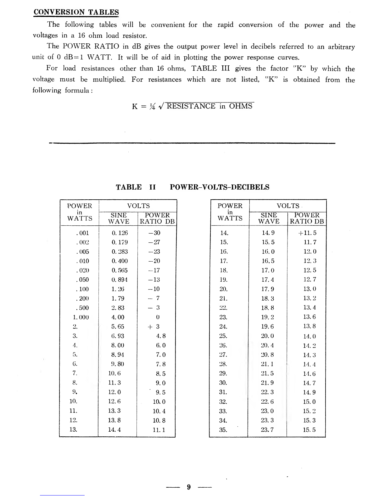
The power output of the amplifier is calculated by the following formula
WATTS output =(Voltage across LOAD RESISTOR)
2
LOAD RESISTOR in OHMS
In measuring the preamplifier response, the output voltage measurements are taken as the
basis in determining the characteristics.
As the input to the amplifier is increased, the power or the voltage readings will increase
linearly to acertain point, after which it will flatten out, indicating overload and consequent
distortion. There will be noticeable distortion when the waveform as observed on the scope just
begins to flatten at both peaks in anormal pushpull amplifier, or one peak in asingle ended
type.
The frequency response of the amplifier is measured by varying the frequency over the
desired range at aconstant input voltage. The output of the LAG-55 is very constant and
usually very slight or no change of the level setting is required as the ranges are changed.
The measurement of the gain and the sensitivity requires the use of aVTVM in the
millivolt range to measure the actual input voltage for aspecified output voltage or power.
In all measurements, excepting the input/output characteristics, care should be taken that
the amplifier is not overloaded by observing the waveforms on the scope.
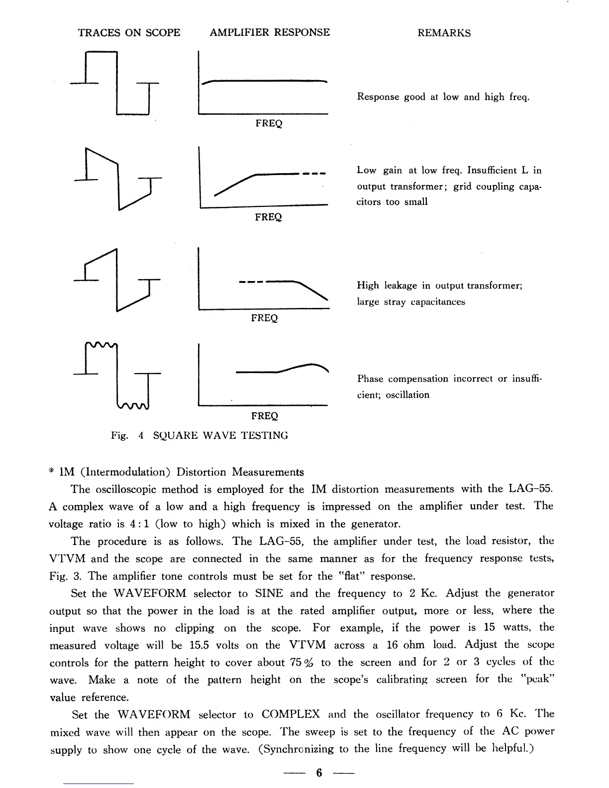
^Square Wave Testing
The testing of the amplifiers by the square waves will reveal many characteristics which
cannot be detected on the response curves.
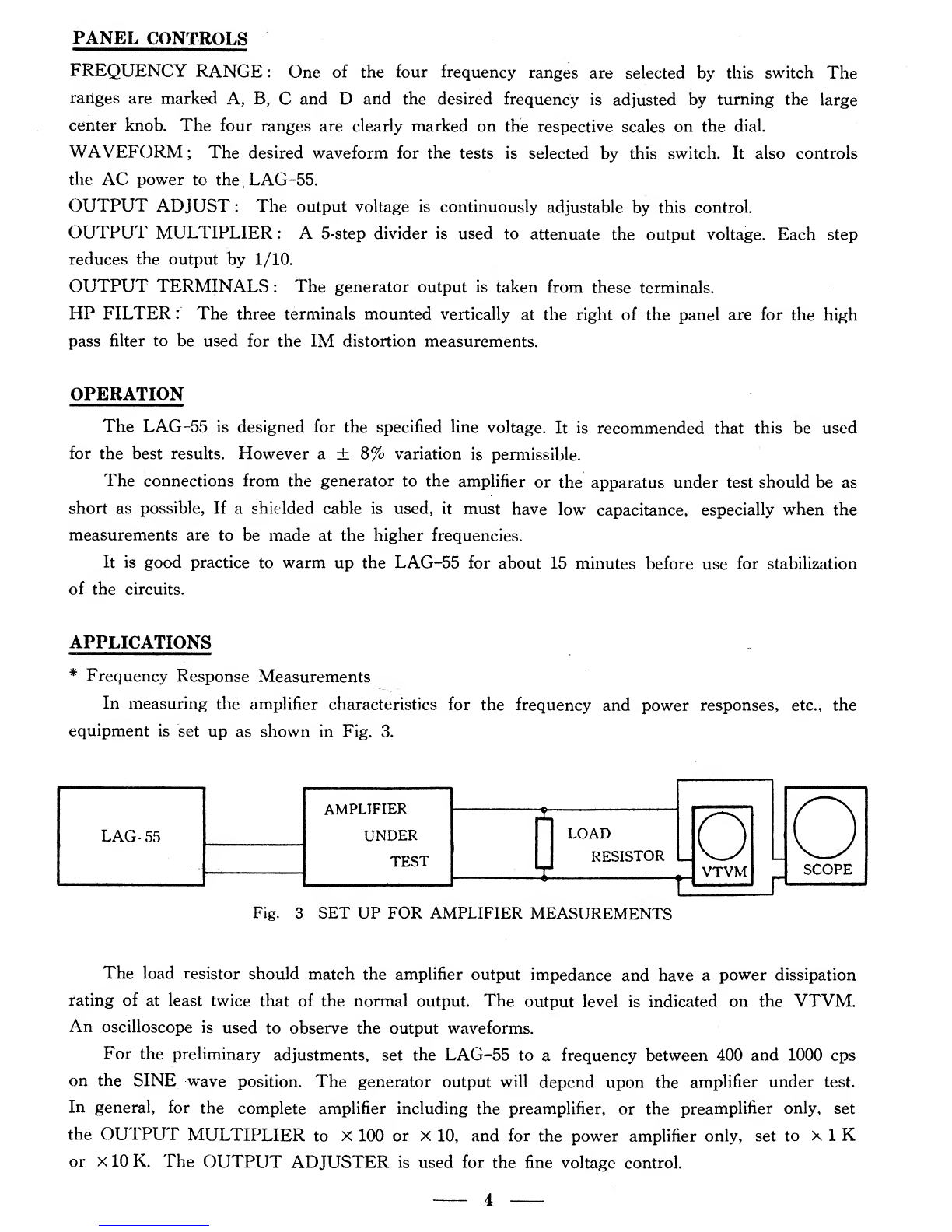
The testing set up is the same as shown in Fig. 3. The LAG-55 is set for the SQUARE
WAVE output, and the frequency is varied from 20 to about 15,000 cps.
In an excellent amplifier, the outp’it waveform will be square without distortion over a
wide range. If there is any fault or defect in its design, the choice of components, etc., the
various wave shapes will give an indication. Some of these waveforms are shown in Fig. 4.
Rapid checking of the frequency response is possible by observing the wave shapes on
the scope. If the low frequency response is poor, there will be adrooping effect. If the high
frequency response is poor, there will be arounding off of the leading edge.
An amplifier with good response will pass square waves over aconsiderable range of fre-
quencies. At the higher frequencies, note the generator frequency where the shape departs from
the square. It is generally accepted that this change will occur at about the ninth or the
eleventh harmonic of the fundamental frequency, or where the \plifier response will start to
fall in a"'flat” amplifier. It the fundamental is say, 2.2 kc then ..le amplifier is "'good” to the
range between about 19 Kc to 24 Kc. The square wave is composed of alarge number of only
the odd-numbered harmonics and this must be borne in mind when testing.
The UvSe of the square waves in the design work will be helpful in checking the performance
of the intermediate amplifier stages, Alow capacitance probe is used for the scope input to
check the various grid, plate and feedback circuits.
It should be noted that tiie square wave input voltage mu.st be kept below the overload
point since the amplifier itself will produce such waves when overloaded.
5

TRACES ON SCOPE AMPLIFIER RESPONSE REMARKS
Response good at low and high freq.
Low gain at low freq. Insufficient Lin
output transformer; grid coupling capa-
citors too small
High leakage in output transformer;
large stray capacitances
Phase compensation incorrect or insuffi-
cient; oscillation
IM (Intermodulation) Distortion Measurements
The oscilloscopic method is employed for the IM distortion measurements with the LAG-55.
Acomplex wave of alow and ahigh frequency is impressed on the amplifier under test. The
voltage ratio is 4:1(low to high) which is mixed in the generator.
The procedure is as follows. The LAG-55, the amplifier under test, the load resistor, the
VTVM and the scope are connected in the same manner as for the frequency response tests,
Fig. 3. The amplifier tone controls must be set for the "flat” response.
Set the WAVEFORM selector to SINE and the frequency to 2Kc. Adjust the generator
output so that the power in the load is at the rated amplifier output, more or less, where the
input wave shows no clipping on the scope. For example, if the power is 15 watts, the
measured voltage will be 15.5 volts on the VTVM across a16 ohm load. Adjust the scope
controls for the pattern height to cover about 75^ to the screen and for 2or 3cycles of the
wave. Make anote of the pattern height oh the scope’s calibrating screen for the "peak”
value reference.
Set the WAVEFORM selector to COMPLEX and the oscillator frequency to 6Kc. The
mixed wave will then appear on the scope. The sweep is set to the frequency of the AC power
supply to show one cycle of the wave. (Synchronizing to the line frequency will be helpful.)
FREQ
6

The generator output is adjusted so that the height of the peaks of this pattern is the same
as the sine wave reference. This step is necessary to equalize the peak outputs for both wave-
forms.
The vertical input lead to the scope is disconnected, from the resistor and connected to
the OUT terminal of the high pass filter. The IN and the Eterminals of the filter are connected
respectively to the high and the low potential terminals of the resistor. See Fig. 5.
Fig. 5IM DISTORTION TEST SET-UP
Adjust the Vertical gain of the scope for the pattern to cover about 50 to 75% of the
screen diameter. DO NOT TOUCH THE AMPLIFIER GAIN CONTROL.
The presence of the IM distortion will be indicated by the notches in the pattern as shown
in Fig. 6. on the right. The depth of the notch is ameasure of the IM distortion. It is calcu-
lated from the formula
Per Cent IM Distortion =—;—rX100
a+b
where aand bare measured on the scope screen.
LOW OR NO IM DISTORTION IM DISTORTION PRESENT
Fig. 6IM DISTORTION PATTERNS
7

APPENDIX
DECIBEL TABLES
The amplifier response/frequency characteristics are plotted on the semi-log section paper.
The output voltage at 400 cps (or IKc) is taken as the reference value. This voltage should
be about 50% of that which produces the rated power or the voltage output. The output
voltage should be recorded for each frequency. The voltage ratio for each reading is computed
by referring to the 400 cps value.
The following table gives the various voltage ratios in decibels. The reader is referred to
the handbooks or texts for more detailed tabulations.
The gain ratio from 1to 10 corresponds to 0to -f20 db, and the loss ratio from 1to 0,1
correspond to 0to —20 dB. The minus sign should not be omitted in the loss measurements.
TABLE IVOLTAGE RATIO-DECIBELS
VOLT RATIO
for LOSS dB
-1-
VOLT RATIO
for GAIN
0. 333 9. 54 3.0
0. 286 10.9 3.5
0. 250 12.0 4.0
0.222 13.0 4.5
0.200 14.0 5.0
0. 182 14.8 5.5
0. 167 15.6 6.0
0. 154 16.2 6.5
0. 143 16.9 7.0
0. 133 17.5 7.5
0. 125 18.0 8.0
0.117 18.6 8.5
0.111 19.1 9.0
0. 105 19.5 9.5
0. 100 20,0 10.0
VOLT RATIO
for LOSS dB
~+
VOLT RATIO
for GAIN
1.00 0, 1.0
0.909 0.828 1,1
0. 833 1.58 1.2
0. 769 2. 28 1.3
0. 714 2. 92 1.4
0.666 3. 52 1.5
0. 625 4.08 1.6
0. 588 4. 61 1.7
0. 555 5. 10 1.8
0. 526 5. 57 1.9
0.500 6, 02 2.0
0. 454 6.85 2.2
0.417 7. 60 2.4
0. 384 8.30 2.6
0.357 8.94 2.8
GAIN RATIO ADD
11 to 100 20 dB
FOR 110 to 1000 40 dB
VOLTAGE 1100 to 10000 60 dB
11000 to 100000 80 dB
RATIOS
OUTSIDE LOSS RATIO ADD
ABOUE RANGE 0. 091 to 0. 01 -20 dB
0. 0091 to 0. 001 ~40 dB
0. 00091 to 0. 0001 -60 dB
0. 000091 to 0. 00001 -80 dB
8

CONVERSION TABLES
The following tables will be convenient for the rapid conversion of the power and the
voltages in a 16 ohm load resistor.
The POWER RATIO in dB gives the output power level in decibels referred to an arbitrary
unit of 0dB —1WATT. It will be of aid in plotting the power response curves.
For load resistances other than 16 ohms, TABLE III gives the factor ''K” by which the
voltage must be multiplied. For resistances which are not listed, is obtained from the
following formula :
K=VRESISTANCE in OHMS“
TABLE II POWER-VOLTS-DECIBELS
POWER
in
WATTS
VOLTS POWER
in
WATTS
VOLTS
SINE
WAVE POWER
RATIO DB SINE
WAVE POWER
RATIO DB
.001 0. 126 1COo14. 14.9 +11.5
.002 0. 179 -27 15. 15.5 11.7
.005 0. 283 -23 16. 16.0 12.0
.010 0. 400 -20 17. 16.5 12. 3
.020 0. 565 -17 18. 17.0 12.5
.050 0. 894 -13 19. 17.4 12.7
.100 1.26 -10 20. 17.9
.200 1.79 -721. 18.3 13.2
.500 2. 83 -322. 18.8 13.4
1. 000 4. 00 023. 19. 213.6
25. 65 +324. 19.6 13.8
3. 6. 93 4.8 25. 20.0 14.0
4.8. 00 6.0 26. 20.4 14.2
5. 8. 94 7.0 27. 20.8 14.3
(3. 9. 80 7.8 28. 21. 114.4
7. 10. 68.5 29. 21.5 14.6
8. 11.3 9.0 30. 21.9 14,7
9. 12.0 9.5 31. 22,3 14.9
10. 12.6 10.. 032. 22.6 15.0
11. 13.3 10.4 33. 23.0 15. 2
12. 13.8 10.8 34. 23.3 15.3
13. 14.4 11.1 35. 23.7 15.5
9

TABLE III VOLTAGE MULTIPLIER
LOAD RESISTOR
in OHMS
~
MUL'ITPLIER
3.2 0. 447
4. 0.500
8. 0.707
12. 0. 865
20. 1. 12
32. 1.42
50. 1.77
100. 2.50
250. 3. 95
600. 6. 13
KXK). 7. 90
2000. 11.2
5000. 17,7
10

LEADER ELECTRONICS CORP.
HEAD OFFICE NO. 850, TSUNASHIMA-CHO, KOHOKU-KU,
YOKOHAMA, JAPAN.
BRANCH OFFICE NO. 4-73, NIHONBASHI-SUJI, NANIWA-KU,
OSAKA, JAPAN.
1966. 8. 500 ®) Printed in Japan.
Table of contents
Other Leader Inverter manuals