LG MG230 User manual

Service Manual Model : MG230/MG235
Service Manual
MG230/MG235
Date: May, 2007 / Issue 1.0
Internal Use Only
Z3X-BOX.COM

LGE Internal Use Only
Copyright © 2007 LG Electronics. Inc. All right reserved.
Only for training and service purposes
- 1 -
* The information in this manual is subject to change without notice and should not be construed as a
commitment by LGE Inc. Furthermore, LGE Inc. reserves the right, without notice, to make changes
to equipment design as advances in engineering and manufacturing methods warrant.
* This manual provides the information necessary to install, program, operate and maintain the
MG230/MG235.
REVISED HISTORY
Editor Date Issue Contents of Changes S/W Version
Y. S. Jeong 2007/01/05 A INITIAL RELEASE
J.M. CHUNG 2007/01/07 A.1
Z3X-BOX.COM

- 2 -
LGE Internal Use Only
Copyright © 2007 LG Electronics. Inc. All right reserved.
Only for training and service purposes
Z3X-BOX.COM

- 3 -
1. INTRODUCTION ...............................5
1.1 Purpose .................................................. 5
1.2 Regulatory Information............................ 5
2. SYSTEM SPECIFICATION................7
3. TECHNICAL BRIEF ..........................8
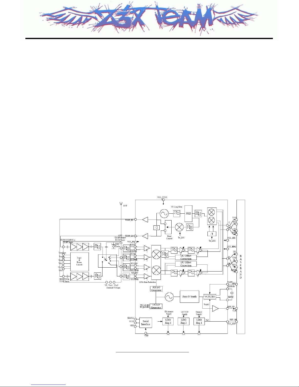
3.1 MG230/MG235 Block diagram.................8
3.2 RF Part Introduction.................................9
3.2.1 Receiver Part ....................................9
3.2.2 Transmitter Part ..............................11
3.2.3 The Crystal Reference System.......13
3.2.4 Power Management........................14
3.3 Baseband Introduction ...........................15
3.3.1 Baseband Processor ......................15
3.3.2 Interconnection with
external devices..............................16
3.3.3 Battery Charging Block ...................19
3.3.4 Display and Interface ......................20
3.3.5 Keypad Switches and Scanning .....22
3.3.6 Microphone .....................................23
3.3.7 Soft-midi and Main Speaker ...........23
3.3.8 Headset Interface ...........................25
3.3.9 Key Back-light Illumination..............26
3.3.10 LCD Back-light Illumination...........27
3.3.11 VIBRATOR ...................................28
4. TROUBLE SHOOTING ...................29
4.1 RF components......................................29
4.2 RX Trouble.............................................30
4.3 TX Trouble .............................................36
4.4 Power On Trouble..................................44
4.5 Charging Trouble ...................................46
4.6 LCD Trouble...........................................48
4.7 Receiver Trouble....................................51
4.8 Speaker Trouble ....................................53
4.9 MIC Trouble ...........................................55
4.10 Earphone Trouble ................................57
4.11 KEYPAD Backlight LEDS Trouble .......61
4.12 SIM Trouble .........................................62
4.13 Vibration Trouble..................................64
5. DOWNLOAD.......................................66
5.1 Download ...............................................66
6. Circuit Diagram ..............................69
7. pcb layout .......................................78
8. ENGINEERING MODE ....................83
8.1 BB Test [MENU 1]..................................82
8.2 RF Test [MENU 2]..................................86
8.3 MF mode [MENU 3] ...............................86
8.4 Trace option [MENU 4] ..........................87
8.5 Call timer [MENU 5] ...............................87
8.6 Fact. Reset [MENU 6] ............................87
8.7 S/W version............................................87
9. STAND ALONE TEST .....................88
9.1 Introduction ............................................88
9.2 Setting Method.......................................88
10. Calibration ....................................91
10.1 Calibration with Hotkimchi....................91
12. EXPLODED VIEW &
REPLACEMENT PART LIST ....... 99
12.1 Exploded View .................................... 99
12.2 Replacement Parts ............................101
12.3 Accessory ......................................... 116
Table Of Contents
LGE Internal Use Only
Copyright © 2007 LG Electronics. Inc. All right reserved.
Only for training and service purposes
Z3X-BOX.COM

- 4 -
LGE Internal Use Only
Copyright © 2007 LG Electronics. Inc. All right reserved.
Only for training and service purposes
Z3X-BOX.COM

- 5 -
1. INTRODUCTION
1.1 Purpose
This manual provides the information necessary to repair, calibration, description and download the
features of the MG230/MG235.
1.2 Regulatory Information
A. Security
Toll fraud, the unauthorized use of telecommunications system by an unauthorized part (for example,
persons other than your company’s employees, agents, subcontractors, or person working on your
company’s behalf) can result in substantial additional charges you’re your telecommunications
services. System users are responsible for the security of own system.
There are may be risks of toll fraud associated with your telecommunications system. System users
are responsible for programming and configuring the equipment to prevent unauthorized use. LGE
does not warrant that this product is immune from the above case but will prevent unauthorized use of
common-carrier telecommunication service of facilities accessed through or connected to it. LGE will
not be responsible for any charges that result from such unauthorized use.
B. Changes in Service
A local telephone company may make changes in its communications facilities or procedure. If these
changes could reasonably be expected to affect the use of the MG230/MG235 or compatibility with the
network, the telephone company is required to give advanced written notice to the user, allowing the
user to take appropriate steps to maintain telephone service.
C. Maintenance Limitations
Maintenance limitations on the MG230/MG235 must be performed only at the LGE or its authorized
agents. The user may not make any changes and/or repairs expect as specifically noted in this
manual. Therefore, note that unauthorized alternations or repair may affect the regulatory status of the
system and may void any remaining warranty.
D. Notice of Radiated Emissions
The MG230/MG235 complies with rules regarding radiation and radio frequency emission as defined
by local regulatory agencies. In accordance with these agencies, you may be required to provide
information such as the following to the end user.
1. INTRODUCTION
LGE Internal Use Only
Copyright © 2007 LG Electronics. Inc. All right reserved.
Only for training and service purposes
Z3X-BOX.COM

- 6 -
1. INTRODUCTION
E. Pictures
The pictures in this manual are for illustrative purposes only; your actual hardware may look slightly
different.
F. Interference and Attenuation
An MG230/MG235 may interfere with sensitive laboratory equipment, medical equipment, etc.
Interference from unsuppressed engines or electric motors may cause problems.
G. Electrostatic Sensitive Devices
ATTENTION
Boards, which contain Electrostatic Sensitive Device (ESD), are indicated by thesign.
Following information is ESD handling:
• Service personnel should ground themselves by using a wrist strap when exchange system boards.
• When repairs are made to a system board, they should spread the floor with anti-static mat which is
also grounded.
• Use a suitable, grounded soldering iron.
• Keep sensitive parts in these protective packages until these are used.
• When returning system boards or parts like EEPROM to the factory, use the protective package as
described.
LGE Internal Use Only
Copyright © 2007 LG Electronics. Inc. All right reserved.
Only for training and service purposes
Z3X-BOX.COM

- 7 -
2. SYSTEM SPECIFICATION
LGE Internal Use Only
Copyright © 2007 LG Electronics. Inc. All right reserved.
Only for training and service purposes
Item Feature Comment
Standard Battery Li-ion, 830mAh
AVG TCVR Current 260 mA typ GSM850@PL5
Standby Current 3.0 mA typ @PP9
Talk time 150 min (GSM850 TX Level 5)
Standby time 200 hours (Paging Period:9, RSSI: -85dBm)
Charging time Under 3 hours
RX Sensitivity GSM850: -105dBm, DCS/PCS : -105dBm
TX Output Power
GSM850: 33dBm (@PL 5)
DCS/PCS: 30dBm (@PL 0)
GPRS compatibility Class 10
SIM card type Yes (SIM Block Type) 3V
Display
Main : 1.51” 128*128 TFT Type
Sub : 96*64 Mono STN
Soft icons, OK, Navigation Key, 0 ~ 9, #,
Status Indicator *,SEND, CLEAR, END/PWR, Volume Up,
Volume Down
ANT Built in antenna
EAR Phone Jack Yes / Jack
PC Synchronization Yes
Speech coding HR/EFR/FR/AMR
Data and Fax Yes
Vibrator Yes
Buzzer No
Voice Recoding Yes
C-Mic Yes
Receiver Yes
Travel Adapter Yes
Options No
Item Feature Comment
Z3X-BOX.COM

- 8 -
3. TECHNICAL BRIEF
3. TECHNICAL BRIEF
LGE Internal Use Only
Copyright © 2007 LG Electronics. Inc. All right reserved.
Only for training and service purposes
3.1 MG230/MG235 Block diagram.
MG230/MG235 is composed with 3 different PCB part such as main PCB, Key FPCB and LCD FPCB.
The functional component arrangement is mentioned below diagram.
Figure 3-1 MG230/MG235 Hardware architecture
Figure 3-2 MG230/MG235 Functional block diagram
Z3X-BOX.COM

- 9 -
3. TECHNICAL BRIEF
3.2. RF Part Introduction
The RF parts consists of a transmitter part, a receiver part, a voltage supply part, the crystal reference
system. And the main RF Chipset AD6548 is a highly integrated direct conversion radio solution that
combines, on a single chip, Quad Band Radio GSM850,E-GSM,DCS1800 and PCS1900 and power
management functions necessary to build the most compact GSM radio solution possible. This quad-
band GSM transmit module integrates a PA, a low-pass filter, a linear Tx / Rx switch along with PA
and switch control combined with ESD protection circuitry in one module,
3.2.1. Receiver Part
The Receiver part in AD6548 contains all active circuits completely, full receiver chain with the
exception of discrete front-end RF SAW filters. The AD6548 uses direct conversion receiver
architecture of the OthelloTM family. For Quad band applicationsthe front end features four fully
integrated programmable gain differential LNAs. The RF is then downconverted by quadrature mixers
and then fed to the baseband programmable-gain amplifiers and active filters for channel selection.
The Receiver output pins can be directly connected to the baseband analog processor.
The Receive path features automatic calibration and tracking to remove DC offsets. The RF Receiver
block is shown as below.
LGE Internal Use Only
Copyright © 2007 LG Electronics. Inc. All right reserved.
Only for training and service purposes
Figure 3-3 The RF Receiver Block
Z3X-BOX.COM

- 10 -
3. TECHNICAL BRIEF
A. Low Noise Amplifiers
The AD6548 includes four fully integrated Low Noise Amplifiers (LNAs), to support quad band
applications without further external active components. The LNAs have differential inputs which
minimize the effect of unwanted interferers. The inputs are easily matched to industry standard FEMs
or discrete Rx SAW filters. The outputs of the LNAs are directly coupled to the down-converting
mixers. The voltage gain of the LNAs are typically 24 dB. Each LNA can be switch to a low gain mode
when receiving large input signals as part of the AGC system.
B. Down-Converting Mixers
Two quadrature mixers are used to mix down the signals from the LNAs, one for the high bands (1800
and 1900 MHz) and one for the low bands (850 and 900 MHz). The outputs of the mixers are
connected to the baseband section through an integrated single pole filter with nominal cut-off
frequency of 800kHz. This acts as a “roofing filter” for the largest blocking signals (i.e. those _ 3MHz)
and prevents the baseband amplifiers from being overloaded.
C. Baseband Amplifiers / Low Pass Filters
The baseband amplifiers provide the majority of the analog receiver gain. The filtering is provided by
an integrated 5th order Chebyshev filter giving the necessary adjacent channel and blocking filtering, it
is also acting as an anti-alias filtering for Baseband IC’s converters. A final low pass pole is possible at
each of the baseband outputs via internal series resistor along with an external shunt capacitor. The
external capacitor is not required with ADI baseband ICs. The on chip filter has an auto calibration
feature ensuring that the filters are tuned for optimum performance. The baseband amplifiers have
programmable gain for system AGC. A total of 57 dB of gain control is provided in 3dB steps
programmable over the serial interface. This together with the LNA gain control gives a total of 77dB of
gain control range. The receive baseband outputs are routed to the common Rx/Tx I/Q ports for
connection with the baseband converters.
D. Baseband Output D.C. Offset Correction
In order to minimize D.C. offsets inherent in the receiver and maximize dynamic range a D.C offset
correction circuit is integrated. This correction is triggered over the serial bus and then an offset
tracking loop is enabled to minimize residual offsets under all conditions. The tracking loop is fully
hardware integrated, requiring no software intervention.
E. Receiver Local Oscillator (LO) Generator
The Rx LO generator is used to avoid DC offset problems associated with LO leakage into the receiver
RF path. By operating the VCO at a frequency other than the desired receive frequencies, any leakage
of the VCO (e.g. via package) will fall out of band. The LO generator is used to convert the offset
synthesized VCO output to the on-frequency quadrature LO required by the chipset. The LO generator
is implemented as a regenerative frequency divider, performing a 2/3 multiplication of the VCO output
for the high band (DCS1800/PCS1900) and a 1/3 multiplication for low band (E-GSM/GSM850).
LGE Internal Use Only
Copyright © 2007 LG Electronics. Inc. All right reserved.
Only for training and service purposes
Z3X-BOX.COM

- 11 -
3. TECHNICAL BRIEF
3.2.2 Transmitter Part
The Transmitter part contains AD6548 active parts and PAM .The transmit section of the AD6548
radio implements a translation loop modulator. This consists of a quadrature modulator, high speed
phase-frequency detector (PFD) with charge pump output, loop filter, TX VCO and a feedback down
converting mixer. The VCO output (divided by 2 for low band) is fed to the power amplifier with a
portion internally fed back into the down-converting feedback mixer to close the feedback loop.
A. Power Amplifier Module
The advanced quad-band Transmit Module designed for mobile handset applications provides full RF
transmit functionality.The GSM850/900 and DCS/PCS power amplifier blocks including power control
are combined with the low insertion loss quad-band pHEMT switch, Tx harmonics filtering, integrated
switch decoder, four receive ports, and full ESD protection. This architecture eliminates the need for
any PA-to-switch design effort for phone designers. All four Rx ports are frequency independent and
allow flexible routing to the transceiver. Fabricated in high-reliability InGaP HBT / pHEMT technology,
the module supports GPRS class 12 operation and provides 50 Ohms input and output impedances at
all RF input and output ports. The module control inputs are CMOS compatible and has no need for an
external reference voltage. With its excellent efficiency performance in all 4 bands, the power amplifier
and switch module contributes to the overall talk-time targets of next generation mobile handset
designs.
B. Quadrature Modulator
The Quadrature modulator takes the baseband I & Q signals and translates these into a GMSK signal
at the Transmit Intermediate Frequency (TX IF). After band-pass filtering and limiting the TX IF signal
is used as the reference input to the Phase Frequency Detector (PFD) of the transmit PLL.
C. Phase Frequency Detector (PFD)
The PFD ensures that the transmitted signal contains the required modulation and is accurately locked
to the desired GSM channel. The downconverted feedback signal from the TXVCO and the
Quadrature Modulator output are phase compared by the PFD. The PFD charge pump generates a
current pulse proportional to the difference in phase which is applied to the loop filter.
D. Loop filter
To minimize complexity of the external PCB layout the TX loop filter is fully integrated into the IC. At
power up the filter is automatically calibrated as part of the baseband filter cal, eliminating process
tolerances. The calibration is fully integrated and requires no extra programming.
E. TX VCO
The Transmit Voltage Controlled Oscillator (TX VCO) and tank components are a fully integrated
subsystem. The subsystem includes PA drivers so the outputs are used to directly drive the external
PAs. The low noise oscillator design and internal filtering mean that external TX SAW filters are not
required. In Low band operation the TX VCO output is divided by two and filtered. The TX VCO is
automatically calibrated to ensure optimum performance over its operating frequency of 1648 to 1910
MHz.
LGE Internal Use Only
Copyright © 2007 LG Electronics. Inc. All right reserved.
Only for training and service purposes
Z3X-BOX.COM

- 12 -
3. TECHNICAL BRIEF
F. Feedback Down-Converting Mixer
The feedback down converting mixer is used to translate the TX VCO output frequency to the TX IF.
An integrated band pass filter exists between the mixer and the PFD to filter the mixers unwanted side
band and higher order mixing products.
G. Transmit Frequency Plan
Unlike many other translation loop modulators the AD6548 uses only a single VCO source to derive
the local oscillator signal for both the Feedback Down-Converting Mixer and the Quadrature
modulator. Therefore there is a fixed relationship between the Tx IF frequency and the LO VCO
frequency .This ratio was chosen to minimize VCO tuning range, TX IF frequency variation and ensure
excellent transmit spectral mask performance. The Feedback-Down Converting Mixer operates low
side injection for the high bands and high side injection for the low bands. The final relationship
between the transmitted TX frequency and the LO VCO frequency is different between the two bands.
These relationships are taken account of in the synthesizer architecture and programming.
H. Main Frequency Synthesizer
The AD6548/9 has a single fast-locking fractional synthesizer used for VCO control in both receive and
transmit mode. The entire system including VCO, tank, fractional N dividers, sigma delta
compensation, charge pump and loop filters are fully integrated. The only external component is a low
cost crystal for the reference. The synthesizer is controlled via the serial interface. The VCO is fed into
the respective dividers to generate the appropriate LO frequencies for the RX and TX bands.
I. Fractional N Dividers
The fractional N divider allows the PLL system to have a smaller step size than the comparison
frequency which is set by the external reference to 26 MHz. This feature allows all the GSM frequency
band rasters to be achieved, with fast lock times and good phase noise characteristics. The divider
section consists of a dual modulus 8/9 pre-scaler, integer M & A dividers, and fractional N system
based on sigma-delta modulation to generate the required fractional divide ratio. The Denominator of
the fractional divider can be set to 3 different values, (1040, 1170,1235), depending on the mode of
operation. For example a denominator of 1040 with an input fraction F maintains an average value of
F/1040 allowing 25 kHz steps when operated at a reference of 26 MHz.
J. Phase Frequency Detector/Charge Pump
A Phase Frequency Detector (PFD) is used for the PLL phase detector. The charge pump is designed
such that good matching of up and down currents is achieved over a wide output operating range. The
charge pump output is internally routed to the integrated synthesizer loop filter.
K. Synthesizer Loop filter
To minimize complexity of the external PCB layout the Main Synthesizer loop filter is also fully
integrated into the IC. No external components or adjustments are required.
LGE Internal Use Only
Copyright © 2007 LG Electronics. Inc. All right reserved.
Only for training and service purposes
Z3X-BOX.COM

- 13 -
3. TECHNICAL BRIEF
L. Voltage Controlled Oscillator
The integrated voltage controlled oscillator (VCO) is a complete self-calibrating subsystem. This
employs a fully automated digital self-calibration function to ensure optimum phase noise performance
over the entire frequency range. The VCO generates frequencies between 2520MHz and 2985MHz as
required to operate in the four bands for RX and TX.
3.2.3 The Crystal Reference System
The AD6548 requires only an external low cost crystal as the frequency reference. The circuitry to
oscillate the crystal and tune its frequency is fully integrated. The Oscillator is a balanced
implementation requiring the crystal to be connected across 2 pins. There is a programmable capacitor
array included for coarse tuning of fixed offsets (e.g. crystal manufacturing tolerance), and an
integrated varactor for dynamic control. The oscillator is designed for use with a 26MHz crystal. The
crystal is connected as shown in figure.
Dedicated control software ensures excellent frequency stability under all circumstances.
LGE Internal Use Only
Copyright © 2007 LG Electronics. Inc. All right reserved.
Only for training and service purposes
Figure 3-4 The Crystal Reference System
Z3X-BOX.COM

- 14 -
3. TECHNICAL BRIEF
3.2.4 Power Management
For direct battery supply connect, and to reduce external circuitry complexity the AD6548/9 features
three Low Drop Out Regulators (LDOs). The three LDOs provide isolation of the oscillators and
sensitive circuits from unwanted power supply and cross coupled noise. They also ensure the IC
operation is robust over a wide range of power supply voltages. For power management the LDOs are
independently controlled via the 3 wire serial bus.
A.LDO Usage
The following table describes the LDO usage:
The LDO outputs require external connection to the respective pins described in table 3, and each
requires decoupling capacitors.The LDOs are designed to be unconditionally stable regardless of the
capacitor’s ESR.
LDO1 derives its input references from the crystal supply voltage (VCC_REF). It is therefore expected
that VCC_REF be supplied from a external LDO of nominal supply voltage 2.75V (e.g. ADP3330 or
Analog Baseband IC: Vout=2.75V_1.4%)
LGE Internal Use Only
Copyright © 2007 LG Electronics. Inc. All right reserved.
Only for training and service purposes
LDO OP Extemal Connection
VLDO1 VCC_FE, VCC_BBI, VCC_BBQ
VLDO2 No external Connections, except for decoupling
VLDO3 No external Connections, except for decoupling
Table 3-2 LDO Connections
Table 3-1 Intended LDO Use
LDO1 LDO2 LDO3
Rx and Tx baseband Main VCO Tx VCO
sections
Z3X-BOX.COM

- 15 -
3. TECHNICAL BRIEF
3.3 Baseband Introduction
3.3.1 Baseband Processor (AD6720 , U101)
• AD6720 is an ADI designed processor
• AD6720 consists of
1. Control Processor Subsystem including:
• 32-bit MCU ARM7TDMI Control Processor
• 39 MHz operation at 1.8V
• 1Mb of on-chip System SRAM Memory
2.DSP Subsystem including:
• 16-bit Fixed Point DSP Processor
• 91 MIPS at 1.8V
• Data and Program SRAM
• Program Instruction Cache
• Full Rate, Enhanced Full Rate and Half Rate
• Speech Encoding/Decoding
• Capable of Supporting AMR & PDC Speech Algorithms
3.Peripheral Functions
• Parallel and Serial Display Interface
• Keypad Interface
• Flash Memory Interface
• Page-Mode Flash Support
• 1.8V and 3.0V, 64 kbps SIM Interface
• Universal System Connector Interface
• Data Services Interface
• Battery Interface (e.g. Dallas)
4. Other
• Supports 13 MHz and 26 MHz Input Clocks
• 1.8V Typical Core Operating Voltages
• 289-Ball Package (12x12mm) , 0.65mm Ball pitch
5. The AD6720 baseband transmit section supports the following
• mobile station GMSK modulation power classes:
• GSM 900/850 power classes 4 and 5,
• DCS 1800 power classes 1 and 2, and
• PCS 1900 power classes 1 and 2
LGE Internal Use Only
Copyright © 2007 LG Electronics. Inc. All right reserved.
Only for training and service purposes
Z3X-BOX.COM

- 16 -
3. TECHNICAL BRIEF
3.3.2 Interconnection with external devices
A. RTC block interface
Countered by external X-TAL
The X-TAL oscillates 32.768KHz
B. LCD module interface
The backlight of LCD module is controlled by AD6720 via AAT3120(U400). The control signals related
to Backlight LED are given bellow.
LGE Internal Use Only
Copyright © 2007 LG Electronics. Inc. All right reserved.
Only for training and service purposes
Signals Description
L_MAIN_LCD_CS MAIN LCD driver chip enable.
L_SUB_LCD_CS SUB LCD driver chip enable.
LCD_RESET This pin resets LCD module.
LCD_WR Enable writing to LCD Driver.
LCD_RS This pin determines whether the data to LCD module data or control data.
LCD_DATA(0-15) LCD data
Table 3-3 LCD Pin Description
Table 3-4 Description Of LCD Backlight LED Control
Signals Description
LCD_DIM_CTL Control LCD backlight level
MLED1,2 Current source for backlight LED
Z3X-BOX.COM

- 17 -
3. TECHNICAL BRIEF
C. RF interface
The AD6720 control RF parts through PA_BAND, TX_RAMP, PA_EN, S_EN, S_DATA, S_CLK,
ANT_SW1, ANT_SW2
D. SIM interface
The AD6720 provides SIM Interface Module. The AD6720 checks status periodically during
established call mode whether SIM card is inserted or not, but it doesn't check during deep Sleep
mode. In order to communicate with SIM card, 3 signals SIM_DATA, SIM_CLK, SIM_RST are
required. The descriptions about the signals are given by bellow Table 3-6 in detail.
LGE Internal Use Only
Copyright © 2007 LG Electronics. Inc. All right reserved.
Only for training and service purposes
Signals Description
PA_BAND PAM Band Select
ANT_SW1, 2 Antenna switch Band Select
TX_RAMP TX RAMP Control
PA_EN PAM Enable/Disable
IQ IQ data(IN, IP, QN, QP)
S_EN PLL Enable/Disable
S_DATA Serial Data to PLL
S_CLK Clock to PLL
Signals Description
SIM_DATA This pin receives and sends data to SIM card. This model can support only
3.0 volt interface SIM card.
SIM_CLK Clock 3.25MHz frequency.
SIM_RST Reset SIM block
Table 3-5 RF Control Signals Description
Table 3-6 SIM Control Signals Description
Z3X-BOX.COM

- 18 -
3. TECHNICAL BRIEF
E. LDO Block
There are 8 LDOs in the AD6720.
- VCORE : supplies Digital base band Processor core and AD6720 digital core
- VMEM : supplies external memory and the interface to the external memory on the digital base band
processor (1,8V or 2.8V, 150mA)
- VEXT : supplies Radio digital interface and high voltage interface (2.8V, 170mA)
- VSIM : supplies the SIM interface circuitry on the digital processor and SIM card(2.85V, 20mA)
- VRTC : supplies the Real-Time Clock module (1.8 V, 20µA)
- VABB : supplies the analog portions of the AD6720
- VMIC : supplies the microphone interface circuitry (2.5 V, 1 mA)
- VVCXO : supplies the voltage controlled crystal oscillator ( 2.75 V, 10 mA)
LGE Internal Use Only
Copyright © 2007 LG Electronics. Inc. All right reserved.
Only for training and service purposes
SIM CONNECTOR
R118
20K
NA
C151
2V85_VSIM
1000p
C150
RST
2
1VCC 5
VPP
ENSY0016601
HSSC-6p-25
J100
3CLK
GND1 4
7GND2
GND3
89
GND4
GND5 10
IO 6
C145
220n
2V85_VSIM
NA
C152
SIM_DATA
SIM_RST
SIM_CLK
Figure 3-5 SIM Interface of AD6720
Z3X-BOX.COM

- 19 -
3. TECHNICAL BRIEF
3.3.3 Battery Charging Block
1. It can be used to charge Lithium Ion batteries.
Charger initialization, trickle charging, and Li-Ion charging control are implemented in hardware.
2. Charging Process
- Check charger is inserted or not
- If AD6720 detects that Charger is inserted, the CC-CV charging starts.
- Exception : When battery voltage is lower than 3.2V, the precharge(low current charge mode)
starts firstly.
- And the battery voltage reach to 3.2V the CC-CV charging starts.
3. Pins used for charging
- VCHG : charger supply.
- GATEDRIVE : charge DAC output
- ISENSE : charge current sense input
- VBATSENSE : battery voltage sense input.
- BATTYPE : battery type identification input
- REFCHG : voltage reference output
4. TA (Travel Adaptor)
- Input voltage: AC 100V ~ 240V, 50~60Hz
- Output voltage: DC 4.8V
- Output current: Max 800mA
5. Battery
- Li-ion battery (Max 4.2V, Nom 3.7V)
- Standard battery: Capacity - 830mAh
LGE Internal Use Only
Copyright © 2007 LG Electronics. Inc. All right reserved.
Only for training and service purposes
CHARGE
(2012,10V) (1608,4V)
VBAT
1uC134
330R120
C137
10u
VCHARGE
0.2
ERHY0001102
R119
EDSY0012101
D101
CUS02
0.1u
R126
C158
82K
T12 VMEMSEL
T13 VRTC
N6 USC5
USC6
N5
B13 VBATSENSE
C12 VCHG
TEMP1
C14
TEMP2
A13
M5 USC0
L3 USC1
M7 USC2
L2 USC3
USC4
M3
D17 REF
REFCHG
F17
REFOUT
C15
U17 KEYON
T16 KEYOUT
LIGHT2
LIGHT3
J15
P8 GPO_22
R5 GPO_23
C13 ISENSE
F4 JTAGEN
GPIO_18
F5
GPIO_20
F6
GPIO_21_TDI
G3
GPIO19_TMS
F2
GATEDRIVE
A12
A14 AUXADC1
AUXADC2
B14
BATTYPE
B12
N11 AGND06
AGND31
F10
AGND04
N9
1
D1
2
D2
D3
36
D4
7
D5
8
D6
4
G
5
S
TPCF8102-TE85L-F
Q102
EQFP0004201
C139
10u
4.7u
R117
C138
C140
2.2K
1u
C136 1u
1V8_VRTC
LCD_DIM_CTL
KEY_BACKLIGHT
TMS
TCK
TDI
TDO1
JTAGEN
USC4
BATT_TEMP
FM_32K
USC0
USC1
USC2
USC3
USC5
KEY_ROW0
POWERKEY
Z3X-BOX.COM
This manual suits for next models
1
Table of contents
Other LG Cell Phone manuals