TABLE
OF
CONTENTS
Section
Title
Page
Tec
PWEBOAR
DS
+:
403
cere.
dn
Geek
FP
gene
41ehs
Glew
wis.
deh
ob
&
ON
OES
ee
Se
ea
ed
ph
Re
ee
4
2.
TEST
EQUIPMENT
FOR
SERVICING...
2.0...
ee
eee
ree
een
ee
beeen
nee
5
3.
AMALIGNMENT
PROCEDURES
..........
0.0...
ccc
cece
een
cence
eee
een
ene
teen
en
eeee
5
S21)
AM
AF
Alignments
«6
63
cies
he
deh
coeds
oe.
wat
when
tteronns
lode
ace
Stet
dk
Shani
et
OMe
te,
Rakha
ee
bie
weed
5
3.2
AM
Frequency
Range
and
Tracking
Alignment...
.
2...
0.0.0
0c
ce
ee
eee
ee
ee
eee
ene
eee
eee
5
3.3
AM
Signal
Strength
Display
Adjustment
......
0.0.0.0
0...
cee
eee
ee
eee
eee
eee
eee
eee
e
een
ees
5
4.
FM
ALIGNMENT
PROCEDURES
...........
0...
ccc
cee
ccc
eee
ence
eee eee
ee
eee
nee
ene
e
enn
5
4.1
IF
Frequency
Range
and
Tracking
Alignment
...
2.2.0.2...
ccc
ce
ee
tee
ee
eee
eee
eee
nee
5
4.2
Stereo
Separation
Alignment
.....
2.0...
0.0.
ee
ee
ce
ee ee
ee
eee
ee
nen
e
eee
ease
eens
.
6
4.3
Muting
Circuit
Alignment...
0...
ec
ee
ee
ee
eee eee
eevee
een
tebe
nba
eeneus
.
6
4.4
Dolby
FM
Tape
QutputSetting
2.0...
ee
ee
ee
ne
eee
en
eee
nee
ene eee
nes
.
6
5.
AUDIO
ADJUSTMENT
2050598
ed
Sain
ehh
ald
etiove
wis ake
ow
dhe
we
eae
ea
dp
see
alah sale
ek
bali
owes
.
6
6.
SCOPE
DISPLAY
ADJUSTMENT...
1.0.0...
.
ec
ee
ee
ee
eee
nee
eee
e
eee
eben
eens
_7
6.1
AM
Tuning
Display
Adjustment
...................0006
adaliaets
ce
We
teht
(pi
ray
Ota
alg
ohies
ant
ne
tee
le
4
She
anes
Ouehe:
bra
ores
.
7
6.2
FM
Tuning
Display
Adjustment
.......0..0.
00.
cece
eee
ec
eee
ee
eee
eee
eee
ene
n
nnn
aenas
od
6.3
FM
Multipath
Display
Adjustment...
0.0.0.0...
00...
cece
ee
ee ee
eee
eee
een
eee
eee
nen
eens
_7
7.
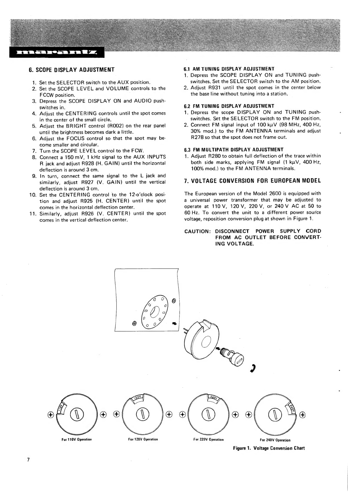
VOLTAGE
CONVERSION
FOR
EUROPEAN
MODEL
........
0...
0.0
ccc
ccc
eee
eee
eee
eee
eens
ae
|
8.
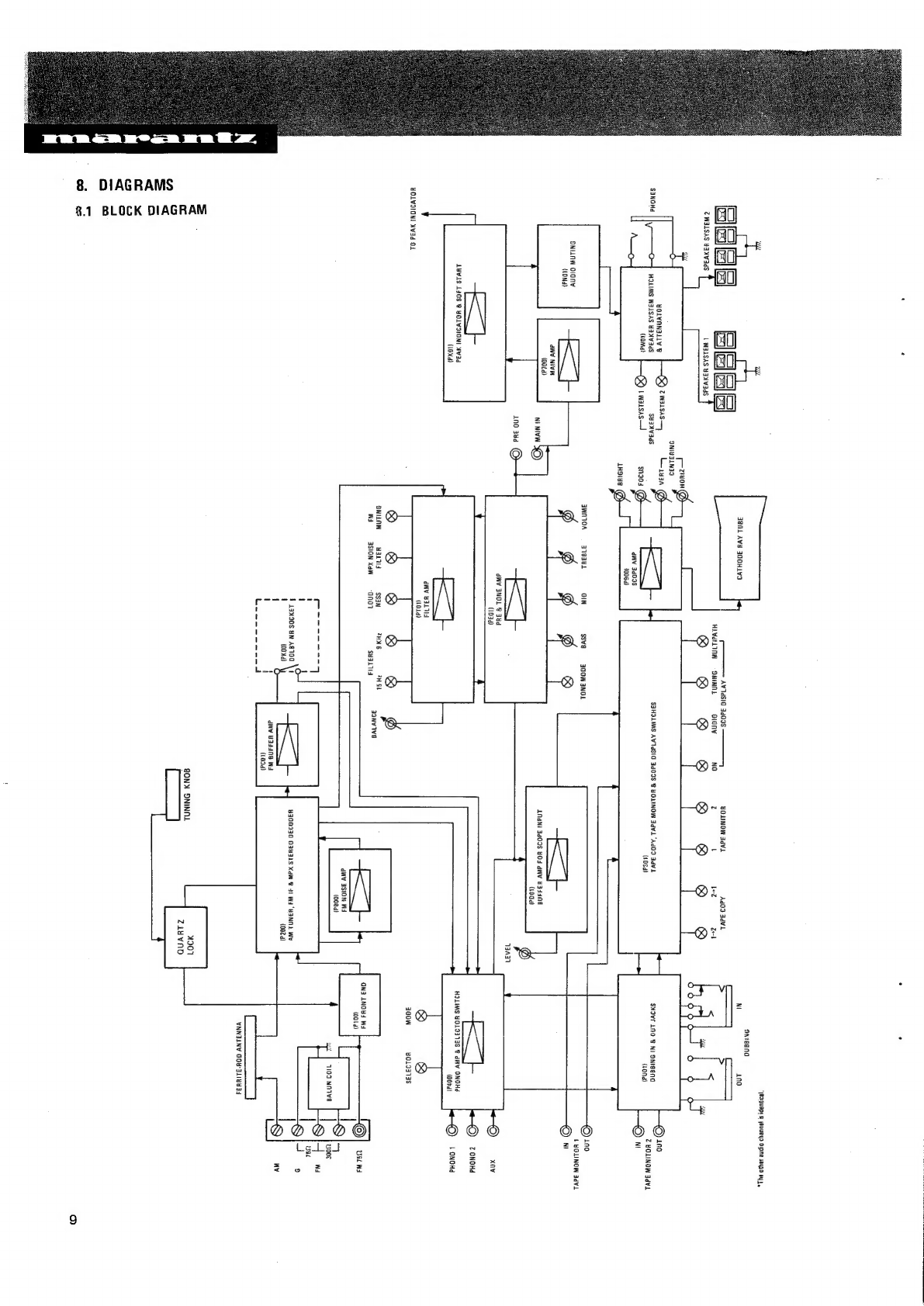
DIAGRAMS
...........
0.
cece
eee
eee
essed
octet
ta
ae
ah
haa
BCetGns
fopton
Sula
ton
Selaawer
eta
mended
¢
Slave
a
aloha
.
9
8.1)
Block:
Diagram.
so
0:0)
2
Raho
cae
e
Wie
Bale
aes,
acho
EG,
wo
Suetee
See
SHS
sarees
bf
iotavtns
b
bled
ow
Male
wel
elated
.
9
8.2
FM
Front
End
Board
Schematic
Diagram
and
Component
Locations-P100..........
0.0.00
eee
eee
uence
eeas
.
10
8.3
AM
Tuner/FM
IF/MPX
Stereo
Decoder
Board
Schematic
Diagram
and
Component
Locations-P200
...............05.
11
8.4
FM
Noise
Amp
Board
Schematic
Diagram
and
Component
Locations-PBOO0
............
0.00
eee
ee
eee
eens
.
14
8.5
FM
Buffer
Amp
Board
Schematic
Diagram
and
Component
Locations-PCO1............
000 cee
eee eee
ees
.14
8.6
Phono
Amp/Selector
Switch
Board
Schematic
Diagram
and
Component
Locations-P400..............-.0-ee008-
.
15
8.7
Power
Supply
Board
Schematic
Diagram
and
Component
Locations
-
P800-U.S.A.&
Canada...
2.20...
ee
ee
ee
.
16
8.8
Power
Supply
Board
Schematic
Diagram
and
Component
Locations
-P800-Europe.............00
eee eee
eens
.17
8.9
Main
Amp
Board
Schematie
Diagram
and
Component
Locations-P700
..
2...
0.00.00.
cee
ee
ee
ee
ee
ees
.
18
8.10
Pre/Tone
Amp
Board
Schematic
Diagram
and
Component
Locations-PEQ1..........-...
000 cee
eee
eee
ees
.
20
8.11
Dolby
NR
Socket
Board
Schematic
Diagram
and
Component
Locations
-
PKO1-
U.S.A.
&
Canada.
...........-..205
.
22
8.12
Audio
Muting
Board
Schematic
Diagram
and
Component
Locations-PNO1..............0.e000e
Spee
e
Yavianiee
anaes
.
22
8.13
Buffer
Amp
for
Scope
Input
Board
Schematic
Diagram
and
Component
Locations-PD01
...............-e.e0008:
-
22
8.14
Tape
Copy/Tape
Monitor/Scope
Display
Switches
Board
Schematic
Diagram
and
Component
Locations-PSO1
...........
-
23
8.15
Dubbing
In/Out
Jacks
Board
Schematic
Diagram
and
Component
Locations-PU01
.........-.-...0c0eeeeaeees
-
23
8.16
Filter
Amp
Board
Schematic
Diagram
and
Component
Locations-PTO1..............-0
cece
cee
eee
neueeens
-
24
8.17
Speaker
System
Switches
/
Attenuator
Board
Schematic
Diagram
and
Component
Locations-PWO1
................
-
25
8.18
Function
Indicator
Board
Schematic
Diagram
and
Component
Locations-PYO01
..............0000e
cee
eeeeeey
-
25
8.19
Dial
Lamp
Board
Schematic
Diagram
and
Component
Locations-PZ01
...
2.0.0.0...
0...
c
ce
eee
eee
cece
ewes
-
25
8.20
Buffer
Amp
Board
Schematic
Diagram
and
Component
Locations-PR50
..
2...
0.00...
00.
cee
eee
ee
ey
-
26
8.21
Scope
Amp
Board
Schematic
Diagram
and
Component
Locations-P900............
0.0000
cee
eee
ee
eee
ees
-
26
8.22
Power
Transistor
Connection
Board
Schematic
Diagram
and
Component
Locations-PM01...........-.-...2-00000,
~
26
8.23
Peak
Indicator/Soft
Start
Board
Schematic
Diagram
and
Component
Locations-PX01
............
0.000
eee
eee
.
27
8.24
Quartz
Lock
Board
Schematic
Diagram
and
Component
Locations-PC50
...........0.-00
2
cee
eee
ee
eee
eee,
-
28
8.25
Touch
Senser
Board
Schematic
Diagram
and
Component
Locations-PK51
..........
0...
e
eee
cece
eee
neces,
-
28
§.
EXPLODED
VIEWS
AND
PARTS
LIST...
.
2.0.0...
0c
ccc
cece
ee
ee
eee
eee
eee
tenn
nee
n
nee,
-
29
9.4:
(C01-99]:
Front:
Panels:
o-oo
ecaresd
te
hace
«bee
teeorg
te
wey
Sta
wee
See
a
wh
pes
ng
obs
SS
Esa
Sees
eked
Sha
an
eles
ha
_
29
9:2:-(C02-99)
Lid:
(Wop:
Cover)
«25.53
eave
cSeas
wd
naa
pees
Aah
My
See
aval
gy
Sen
Wuaa
temeae
elon
euoth
vee
wee
eee
_
30
9.3
[CO3-99]
Rear
Panel...
2...
Lc
ee
eee
cence
eee
te
nee
eben
teenies
-
3i
9.4
[P01-99]
Front
Chassis
and
General
Parts
22...
2.0...
cee
ee
eee
eee
enna
tees
Biles
ten
seit
ot
ea
.
33
9.5
[P02-99]
Assembled
P.W.
Boards
and
Other
Parts...
2.2...
0.
cee
eee
eee
cece
eee
eee
eens,
_
34
9.6
[P03-99]
Power
Transistor
and
Heatsink
2.0...
ce
cee
eee
eee eee
n
eet
nnnes,
_
35