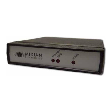
Midian Electronics BTD-1A User manual

1
BTD-1A
Burst Tone Decoder – 1200-2600 Hz
BTD-1B
Burst Tone Decoder – 700-3000 Hz
Manual Revision: 2012-10-19

2
SPECIFICATIONS
Operating Voltage +5.5-15 VDC
Operating Current 3 mA
Operating Temperature -30 - +60 C
Dimensions 1.87” L x 1.0” W x 0.34” H
BTD-1A - Frequency Range 1200-2600 Hz
BTD-1B - Frequency Range 700-3000 Hz
Band Width 0.5%
Input Level 10 mV-2.0 V RMS
Input Impedance 100 k
Momentary/Latched Output Current 200 mA
Ringing Output 2400 Hz
Detect/Release Time 20 ms-1/5 sec
GENERAL INFORMATION
Midian’s BTD-1 product is a burst tone decoder that can decode a burst tone or continuous tone. Decades ago
before CTCSS and DCS, burst tone was the common method of granting access to repeaters. Nowadays, the
BTD-1 is largely used as a continuous tone decoder for 2175 Hz or other tones.

3
HARDWARE INSTALLATION
Be certain to follow standard anti-static procedures when handling any of Midian’s products.
P1-1 – Green – Transpond Out – Provides a low output (200mA) approximately 2 seconds after the horn output.
P1-2 – Red - +5.5 – 15 VDC – Connect to switched B+ in the radio.
P1-3 – Brown – Repeater Output: Provides a low output when decode occurs. This output floats when carrier is
removed. See P1-7 positive and negative squelch inputs.
P1-4 – Black – Ground – Connect to the nearest ground point.
P1-5 – Blue – Alert Tone Output (Lo Z) – Provides a tone output (2400Hz) for approximately 2 seconds upon
decoding.
P1-6 – Orange – Audio Input – Connect to an unsquelched audio point in the receiver. Usually the discriminator
or volume control high. Note: The input audio level is adjusted by changing the value of R4. See gain chart on
schematic.
P1-7 – Yellow – Positive or Negative Squelch Input – With JU5 installed, connect to a point in the receiver
squelch circuit that is high when a carrier is present and low when the carrier is missing. With JU6 installed,
connect to a point in the receiver that is low when a carrier is present and high when the carrier is missing.
Repeater knock down will occur when the carrier is removed.
P1-8 – Green/White – Squelch Output – Connect to the radio squelch circuit to mute the radio until decode
occurs. Provides a high output until decode, then a float is present with JU3 installed. With JU4 installed a low
output is provided via D9 from U2C Pin 14.
P1-9 – White – Call Light Output – Provides a latched low output (200mA).
P1-10 – Gray/White – Horn Output – Provides a low (200mA) output for approximately 4 seconds after decode.
P1-11 – Gray – Monitor 2 Input – Remove JU2. Connect grey/white lead to a point in the radio that is normally
low and goes high or to a float when PTT is pressed. A return to a low when PTT is released will reset the
squelch outputs.
P1-12 – Orange/White – Monitor 1 Input – Connect to a point in the radio that goes high when PTT is pressed.
The squelch outputs will not be reset when the PTT is released.
P1-13 – Violet – Alert Tone Output (Hi Z) – Provides a tone output (2400Hz) for approximately 2 seconds upon
decoding.

4
HARDWARE ALIGNMENT
The frequency of the BTD-1 is set using one of two methods:
Method 1
Install JU1 and, while monitoring Pin 7 of U1C with a frequency counter, adjust R15 to the desired frequency.
Remove JU1.
Method 2
Inject an audio signal, at the proper amplitude, on the desired burst tone frequency into the orange lead. While
observing Pin 7 of U1C with a scope, adjust R15 for a peak in amplitude.
The Bandwidth is set by injecting the signal into the orange lead, as above, except set the frequency .25% away
from the desired burst tone frequency. While monitoring Pin 7 of U2B, adjust R25 until Pin 7 goes high.
R34 adjusts the tone decode time before actuation of any of the BTD-1 outputs. (This delay is used to prevent
falsing due to short duration audio signals entering the decoder.)
R11 adjusts the amount of negative or positive squelch input voltage that is required to disable the repeater
output lead when the carrier is no longer present. Most newer radios use TTL 5 volt logic levels but a lot of older
radios may only change a few tenths of a volt. Set R11 for your particular circumstance.
U3F with R19 and C6 acts as a hang timer after the loss of carrier signal on Pin 7 yellow squelch lead. When this
timer times out it causes U3 to generate a reset pulse on U2C turning off the repeater output.
Continuous Decode
The BTD-1 has the trace IC2 pin 14 to R37 cut with a jumper from IC2 pin 7 to R37 installed. As long as the BTD-
1 receives a continuously programmed tone the unit will turn on the Repeater Out transistor causing its output to
go low (brown wire).

5
CIRCUIT DESCRIPTION
The single tone is input on the orange lead and passes through C1 to the input of U1A, which amplifies the input
tone. R4 may be adjusted to change the sensitivity of the unit. The tone then passes through R5 to the active
filter circuit of U1B, U1C, and U1D. The output on Pin 7 of U1C is passed through R22 to detector U2A. The
output of U2A passes through D4 and R30 to the input of comparator U2B. The comparator's window is set by
adjusting R25 (bandwidth) to produce the proper trigger voltage on U2B, Pin 6.
R34, when adjusted, provides a variable delay from the moment of decode to the time the various outputs are
activated. The output of U2B, Pin 7 goes high when the proper burst tone is detected, and D3A is then back
biased. C13 then charges, triggering U3A. The output of U3A goes low, producing a pulse through C14, turning
off U3B for four seconds, and producing a high on its output.
The high output on U3B turns on Q1 for four seconds, causing a low output on the grey/white Pin 10 horn output
wire. When U3A triggers, a 2400 Hz alert tone is produced on the blue lead, Pin 5, and violet lead, Pin 13, and
after 2 seconds, a low transpond output is produced on the green lead, Pin 1, for approximately 2 seconds.
The high output of U3B is also passed to the input of latch U2C. U2C turns on, producing a high output that turns
on Q3, which creates a low call light output on the white lead, Pin 9, & back biases D8, producing a float output on
the normally high green/white lead positive squelch output via JU3.
A high input on the orange/white monitor 1 input lead, Pin 12, latches U2C. The monitor 2 input on the grey lead,
Pin 11, is normally grounded, through JU2. If JU2 (ground) is removed, a transition from a low to a high or float
on the monitor 2 input lead produces monitoring. When the input returns to low, the white call light lead, Pin 9,
the brown repeater out lead, Pin 3, and the green/white radio squelch lead, Pin 8, are reset.
The negative and positive squelch inputs are used if the BTD-1 is to be used in a radio repeater. The transition
from a low on the yellow lead, Pin 7, via JU6 for the negative squelch input or a high on the yellow lead via JU5
for the positive squelch polarity, or a float, will turn off Q4, and the brown repeater output lead, Pin 3, will float.
The white call light lead, Pin 9, and the green/white squelch output lead, Pin 8, will also reset.
MIDIAN CONTACT INFORMATION
MIDIAN ELECTRONICS, INC.
2302 East 22nd Street
Tucson, Arizona 85713 USA
Toll-Free: 1-800-MIDIANS
Main: 520-884-7981
E-mail: sales@midians.com
Web: www.midians.com
- This page intentionally left blank-

1
1
2
2
3
3
4
4
5
5
6
6
D D
C C
B B
A A
-
+
2
3
1
U2:1
-
+
6
5
7
U2:2
-
+
9
10
8
U2:3
-
+
13
12
14
U2:4
-
+
13
12
14
U1:1 -
+
2
3
1
U1:2
-
+
6
5
7
U1:3
-
+
9
10
8
U1:4
200K
R1
240K
R2
240K
R3
18K
R4
820K
R5
100K
R6
.01u
C1
VAN
VAN
2.4K
R7
7.5K
R16
100K1%
R17
240K
R18
5.6K
R20
VAN
560p
C5
VAN
.001u
C4
100K1%
R21
47K
R22
47K
R29
2.7K
R50
100K
R28
100K
R27
10K
R26
43K
R30
VAN
.001u
C10
VAN
2 1
A6
D4:1
+5V
.1u
C11
GND
+5V
1.8M
R31
11
33
22
10K
R25
GND
10K
R36
10K
R35
AKK
A7
D3:1
A AK
A7
D3:2
11 33
22
1M
R34
+5V
+
4.7u
C13
GND
1 2
U3:1
3 4
U3:2
5 6
U3:3
9 8
U3:4
11 10
U3:5
13 12
U3:6
+
.47u
C14
+5V
820M
R39
+5V
47K
R38
D25
Q1
2 3
A6
D6:1
GND GND
K AK
A6
D2:1
AAK
A6
D2:2
A4
32
D1:1
A4
13
D1:2
100K
R23
+5V
.01u
C9
.1u
C8
GND
GND
A4
2 3
D7:2
A4
3 1
D7:1
+
.47u
C15
+5V
4.7M
R41
GND
10K
R40
B25
Q2
.01u
C16
+
.1u
C17
220K
R42
47K
R43
GRAY/WHT
P1:1
TRANSPOND OUT
RED
P1:2
+VIN +5.5 - 15V
BROWN
P1:3
REPEATER OUT
BLACK
P1:4
GROUND
BLUE
P1:5
LO Z
ORG
P1:6
TONE IN
YEL
P1:7
SQUELCH IN
GRN/WHT
P1:8
+/- SQUELCH OUT
WHITE
P1:9
CALL OUT
GRAY/WHT
P1:10
HORN OUT
GRAY
P1:11
MONITOR 2
ORG/WHT
P1:12
MONITOR 1
VIOLET
P1:13
HI Z
GND
VAN
+
.1u
C2
+
.1u
C3
*
R8
10K
R10
10K
R12
330K
R14
11
33
22
10K
R11
GND
GND
GND
+5V
+5V
2 3
A6
D13:1
2 1
A6
D13:2
+
4.7u
C6
820K
R19
GND GND
.1u
C7
.01u
C12
1M
R24
100K
R33
2.4K
R45
100K
R32
1M
R48
2 3
A6
D12:1
2 1
A6
D12:2
A4
32
D11:1
A4
1 3
D11:2
GND GND
+5V
B25
Q3
A4
32
D9:1
A4
1 3
D9:2
100K
R44
+VIN
GND
47K
R37
D25
Q4
GND
2 3
A6
D10:1
1 3
A6
D10:2
GND
23
A6
D8:1
13
A6
D8:2
LP2951
VR1
+VIN
.022u
C18
GND
GND
+5V
10K
R46
10K
R47
GND GND GND
VAN
+5V
21
JU1
21
JU2
21
JU3
21
JU4
21
JU5
21
JU6
2 3
A6
D4:2
+
.47u
C19
+
.47u
C20
1 3
A6
D6:2
A4
13
D5:2 A4
3 1
D5:1
11 33
22
10K
4R15
VAN
CP
K.K.
1986-10-28 DML
2012-04-13
B-4
1 of 1 7232
MIDIAN ELECTRONICS, INC.
DATE:
DESIGN:
DWN BY:
REV:
APPR
COPYRIGHT © 2012
REV
SHEET PROJECT NUMBER
DOCUMENT NAME
SCHEMATIC
BTD-1-A
NOTES
A B
R16
R20
7.5K 1.8K
5.6K 2.7K
10-50mV RMS
50-500mV RMS
500-1000mV RMS
TONE IN LEVEL R4 GAIN ADJ
1K
22K
OMIT R4

- This page intentionally left blank-


1
1
2
2
3
3
4
4
5
5
6
6
D D
C C
B B
A A
-
+
2
3
1
U2:1
-
+
6
5
7
U2:2
-
+
9
10
8
U2:3
-
+
13
12
14
U2:4
-
+
13
12
14
U1:1 -
+
2
3
1
U1:2
-
+
6
5
7
U1:3
-
+
9
10
8
U1:4
200K
R1
240K
R2
240K
R3
18K
R4
820K
R5
100K
R6
.01u
C1
VAN
VAN
2.4K
R7
1.8K
R16
100K1%
R17
240K
R18
2.7K
R20
VAN
560p
C5
VAN
.001u
C4
100K1%
R21
47K
R22
47K
R29
2.7K
R50
100K
R28
100K
R27
10K
R26
43K
R30
VAN
.001u
C10
VAN
2 1
A6
D4:1
+5V
.1u
C11
GND
+5V
1.8M
R31
11
33
22
10K
R25
GND
10K
R36
10K
R35
AKK
A7
D3:1
A AK
A7
D3:2
11 33
22
1M
R34
+5V
+
4.7u
C13
GND
1 2
U3:1
3 4
U3:2
5 6
U3:3
9 8
U3:4
11 10
U3:5
13 12
U3:6
+
.47u
C14
+5V
820M
R39
+5V
47K
R38
D25
Q1
2 3
A6
D6:1
GND GND
K AK
A6
D2:1
AAK
A6
D2:2
A4
32
D1:1
A4
13
D1:2
100K
R23
+5V
.01u
C9
.1u
C8
GND
GND
A4
2 3
D7:2
A4
3 1
D7:1
+
.47u
C15
+5V
4.7M
R41
GND
10K
R40
B25
Q2
.01u
C16
+
.1u
C17
220K
R42
47K
R43
GRAY/WHT
P1:1
TRANSPOND OUT
RED
P1:2
+VIN +5.5 - 15V
BROWN
P1:3
REPEATER OUT
BLACK
P1:4
GROUND
BLUE
P1:5
LO Z
ORG
P1:6
TONE IN
YEL
P1:7
SQUELCH IN
GRN/WHT
P1:8
+/- SQUELCH OUT
WHITE
P1:9
CALL OUT
GRAY/WHT
P1:10
HORN OUT
GRAY
P1:11
MONITOR 2
ORG/WHT
P1:12
MONITOR 1
VIOLET
P1:13
HI Z
GND
VAN
+
.1u
C2
+
.1u
C3
*
R8
10K
R10
10K
R12
330K
R14
11
33
22
10K
R11
GND
GND
GND
+5V
+5V
2 3
A6
D13:1
2 1
A6
D13:2
+
4.7u
C6
820K
R19
GND GND
.1u
C7
.01u
C12
1M
R24
100K
R33
2.4K
R45
100K
R32
1M
R48
2 3
A6
D12:1
2 1
A6
D12:2
A4
32
D11:1
A4
1 3
D11:2
GND GND
+5V
B25
Q3
A4
32
D9:1
A4
1 3
D9:2
100K
R44
+VIN
GND
47K
R37
D25
Q4
GND
2 3
A6
D10:1
1 3
A6
D10:2
GND
23
A6
D8:1
13
A6
D8:2
LP2951
VR1
+VIN
.022u
C18
GND
GND
+5V
10K
R46
10K
R47
GND GND GND
VAN
+5V
21
JU1
21
JU2
21
JU3
21
JU4
21
JU5
21
JU6
2 3
A6
D4:2
+
.47u
C19
+
.47u
C20
1 3
A6
D6:2
A4
13
D5:2 A4
3 1
D5:1
11 33
22
10K
4R15
VAN
CP
K.K.
1986-10-28 DML
2012-04-13
B-4
1 of 1 7232
MIDIAN ELECTRONICS, INC.
DATE:
DESIGN:
DWN BY:
REV:
APPR
COPYRIGHT © 2012
REV
SHEET PROJECT NUMBER
DOCUMENT NAME
SCHEMATIC
BTD-1-B
NOTES
A B
R16
R20
7.5K 1.8K
5.6K 2.7K
10-50mV RMS
50-500mV RMS
500-1000mV RMS
TONE IN LEVEL R4 GAIN ADJ
1K
22K
OMIT R4

- This page intentionally left blank-


This manual suits for next models
1
Table of contents
Other Midian Electronics Media Converter manuals

Midian Electronics
Midian Electronics VTE-1 User manual

Midian Electronics
Midian Electronics TS-120-VX1 User manual

Midian Electronics
Midian Electronics TTD-5 User manual

Midian Electronics
Midian Electronics MTSD-3 User manual

Midian Electronics
Midian Electronics ANI-F Maxon User manual

Midian Electronics
Midian Electronics ANI-F User manual

Midian Electronics
Midian Electronics TRE-2 User manual