manuals.online logo
Brands
  1. Home
  2. •
  3. Brands
  4. •
  5. Murata
  6. •
  7. Industrial Electrical
  8. •
  9. Murata GRM31CC80G157ME11 Series User manual

Murata GRM31CC80G157ME11 Series User manual

This manual suits for next models

9

Other Murata Industrial Electrical manuals
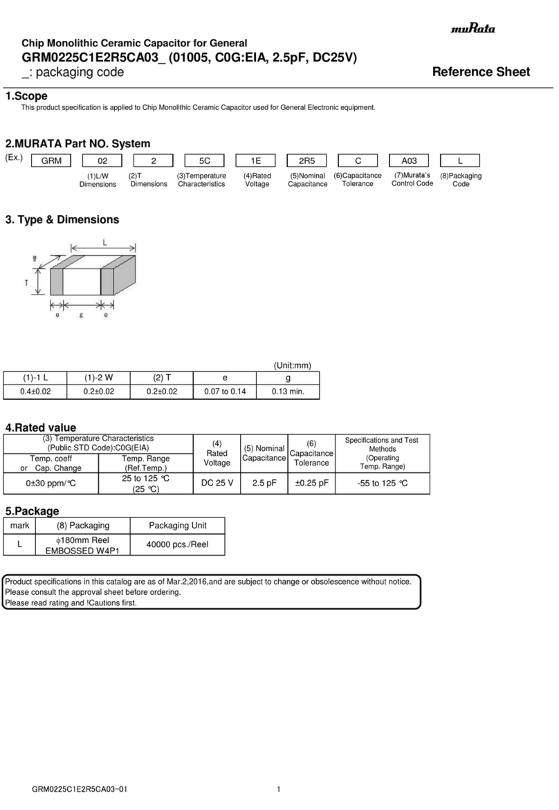
Murata GRM0225C1E100JA03 Series User manual

Murata

Murata GRM0225C1E100JA03 Series User manual

Murata GRM1885C1H160JA01 Series User manual

Murata

Murata GRM1885C1H160JA01 Series User manual

Murata GJM0335C1HR27WB01 Series User manual

Murata

Murata GJM0335C1HR27WB01 Series User manual

Murata GRM1555C1H6R2WA01 Series User manual

Murata

Murata GRM1555C1H6R2WA01 Series User manual

Murata GQM22M5C2H1R2BB01 Series User manual

Murata

Murata GQM22M5C2H1R2BB01 Series User manual

Murata GRT155R61C224ME01 Series User manual

Murata

Murata GRT155R61C224ME01 Series User manual

Murata GRM0335C1H7R2BA01 Series User manual

Murata

Murata GRM0335C1H7R2BA01 Series User manual

Murata GRJ32DC72A475KE11 Series User manual

Murata

Murata GRJ32DC72A475KE11 Series User manual

Murata GJM0335C1E6R2BB01D User manual

Murata

Murata GJM0335C1E6R2BB01D User manual

Murata GRM1555C1H2R0BA01 Series User manual

Murata

Murata GRM1555C1H2R0BA01 Series User manual

Murata GRM0335C1H6R9DA01 Series User manual

Murata

Murata GRM0335C1H6R9DA01 Series User manual

Murata GRM1555C1E751JA01 Series User manual

Murata

Murata GRM1555C1E751JA01 Series User manual

Murata GRM2165C2A201JA01 Series User manual

Murata

Murata GRM2165C2A201JA01 Series User manual

Murata GRM0225C1E1R0BA03 Series User manual

Murata

Murata GRM0225C1E1R0BA03 Series User manual

Murata GRM216R71H302JA01 Series User manual

Murata

Murata GRM216R71H302JA01 Series User manual

Murata GRM0335C1H8R0DA01 Series User manual

Murata

Murata GRM0335C1H8R0DA01 Series User manual

Murata GRM155R71A683KA01 Series User manual

Murata

Murata GRM155R71A683KA01 Series User manual

Murata GRM31CR60J476KE19 Series User manual

Murata

Murata GRM31CR60J476KE19 Series User manual

Murata GQM1885C1H120GB01 Series User manual

Murata

Murata GQM1885C1H120GB01 Series User manual

Murata GJM1555C1H3R3DB01 Series User manual

Murata

Murata GJM1555C1H3R3DB01 Series User manual

Murata GRM0335C1H5R6BA01 Series User manual

Murata

Murata GRM0335C1H5R6BA01 Series User manual

Murata GJM0225C1E7R1CB01 Series User manual

Murata

Murata GJM0225C1E7R1CB01 Series User manual

Murata GRM31C5C1H104JA01 Series User manual

Murata

Murata GRM31C5C1H104JA01 Series User manual

Murata GJM0335C1E9R5DB01 Series User manual

Murata

Murata GJM0335C1E9R5DB01 Series User manual

Popular Industrial Electrical manuals by other brands
ARCAIR N6000 Automatic System Safety and operating instructions

ARCAIR

ARCAIR N6000 Automatic System Safety and operating instructions

MFJ MFJ-918 quick start guide

MFJ

MFJ MFJ-918 quick start guide

Abtech HVJB Series Installation, operation & maintenance instructions

Abtech

Abtech HVJB Series Installation, operation & maintenance instructions

SAF-HOLLAND CBX 5415.5 Installation and operation manual

SAF-HOLLAND

SAF-HOLLAND CBX 5415.5 Installation and operation manual

Eaton Ulusoy HMH24-04 user manual

Eaton

Eaton Ulusoy HMH24-04 user manual

Newlong NP-7H NSTRUCTION MANUAL/PARTS LIST

Newlong

Newlong NP-7H NSTRUCTION MANUAL/PARTS LIST

Stahl 8575/12 operating instructions

Stahl

Stahl 8575/12 operating instructions

SI Pegasus installation instructions

SI

SI Pegasus installation instructions

Cooper Power Systems VXE15 Installation and operation instructions

Cooper Power Systems

Cooper Power Systems VXE15 Installation and operation instructions

S&C Vista SD manual

S&C

S&C Vista SD manual

Siemens 3VA9988-0BM10 operating instructions

Siemens

Siemens 3VA9988-0BM10 operating instructions

Siemens SITRANS LVS100 operating instructions

Siemens

Siemens SITRANS LVS100 operating instructions

Rockwell Automation Allen-Bradley MP-Series installation instructions

Rockwell Automation

Rockwell Automation Allen-Bradley MP-Series installation instructions

Phasemation DG-100 owner's manual

Phasemation

Phasemation DG-100 owner's manual

ABB System pro E power Instruction handbook

ABB

ABB System pro E power Instruction handbook

WPI STX2-PLUS instruction manual

WPI

WPI STX2-PLUS instruction manual

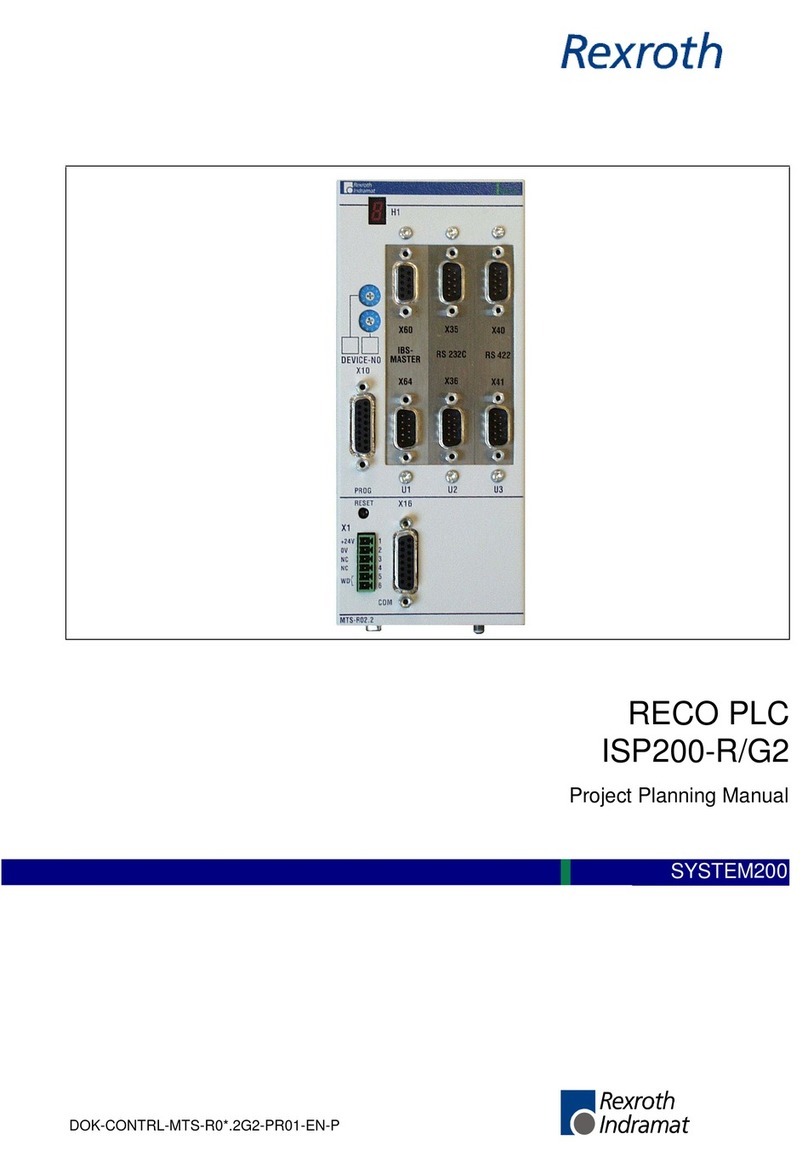
Rexroth Indramat DURADRIVE SYSTEM200 Project planning manual
Rexroth Indramat

Rexroth Indramat DURADRIVE SYSTEM200 Project planning manual

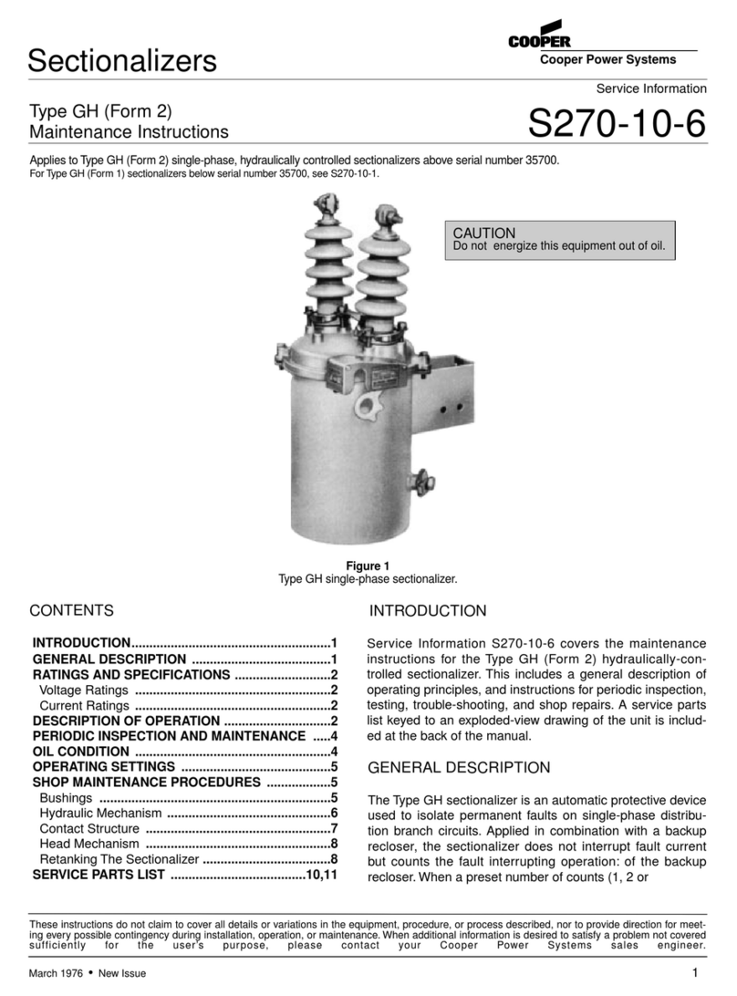
Cooper Power Systems GH Maintenance instructions

Cooper Power Systems

Cooper Power Systems GH Maintenance instructions

manuals.online logo
manuals.online logoBrands
  • About & Mission
  • Contact us
  • Privacy Policy
  • Terms and Conditions

Copyright 2025 Manuals.Online. All Rights Reserved.

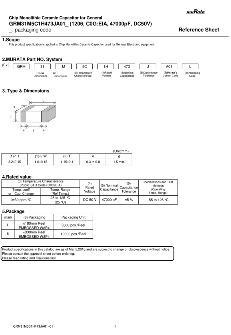
GRM31CC80G157ME11_ (1206, X6S:EIA, 150uF, DC4V)
_: packaging code Reference Sheet
1.Scope
  
2.MURATA Part NO. System
(Ex.)
3. Type & Dimensions
(Unit:mm)
4.Rated value
5.Package
Product specifications in this catalog are as of Mar.5,2016,and are subject to change or obsolescence without notice.
Please consult the approval sheet before ordering.
Please read rating and !Cautions first.
(3) Temperature Characteristics
(Public STD Code):X6S(EIA)
g
0.3 to 0.9
(5) Nominal
Capacitance
mark
(4)
Rated
Voltage
Packaging Unit
DC 4 V
Temp. Range
(Ref.Temp.)
(8) Packaging
-22 to 22 %
-55 to 105 °C
(25 °C)
1.5 min.
(1)-1 L
3.2±0.3
(1)-2 W
1.6±0.3
This product specification is applied to Chip Monolithic Ceramic Capacitor used for General Electronic equipment.
(2) T
e
Chip Monolithic Ceramic Capacitor for General
Specifications and Test
Methods
(Operating
Temp. Range)
Temp. coeff
or Cap. Change
±20 %
(6)
Capacitance
Tolerance
150 uF
1.6±0.3
-55 to 105 °C
L
f180mm Reel
EMBOSSED W8P4
2000 pcs./Reel
K
f330mm Reel
EMBOSSED W8P4
6000 pcs./Reel
(1)L/W
Dimensions
(2)T
Dimensions
(3)Temperature
Characteristics
(4)Rated
Voltage
(5)Nominal
Capacitance
(6)Capacitance
Tolerance
(8)Packaging
Code

Control Code
GRM 31 CC8 0G 157 M E11 L
GRM31CC80G157ME11-01 1
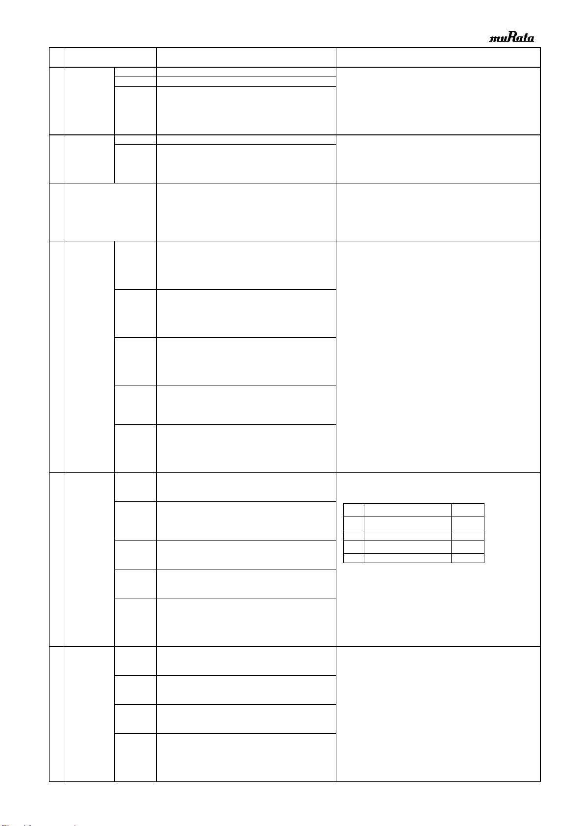
■Specifications and Test Methods
No
1 Rated Voltage Shown in Rated value. The rated voltage is defined as the maximum voltage which may be
applied continuously to the capacitor.
When AC voltage is superimposed on DC voltage, VP-P or VO-P,
whichever is larger, should be maintained within the rated voltage
range.
2 Appearance No defects or abnormalities. Visual inspection.
3 Dimension Within the specified dimensions. Using calipers. (GRM02 size is based on Microscope)
4 Voltage proof No defects or abnormalities.
Measurement Point   :
Between the terminations
Test Voltage        :
250% of the rated voltage
Applied Time :
1 to 5 s
Charge/discharge current :
50mA max.
5 Insulation Resistance(I.R.) 
Measurement Point   : Between the terminations
Measurement Voltage :
DC Rated Voltage
Charging Time :
1 min
Charge/discharge current :
50mA max.
Measurement Temperature :
Room Temperature
6 Capacitance Shown in Rated value.
Measurement Temperature :
Room Temperature
7 Dissipation Factor (D.F.) B1,R1,B3,R6,R7,C6,C7,C8,E7,D7 : 0.1 max.
D8,GRM31CR60J107 : 0.15 max
GRM31CR71E106 : 0.125
max
*1 For items listed in Table 1 on the left, the capacitance should
be measured using a voltage of 0.5+/-0.1Vrms instead of
1.0+/-0.2Vrms.
*2 For item GRM188R70J105, the capacitance should be measured
using a voltage of 1.0+/-0.2Vrms instead of 0.5+/-0.1Vrms.
8
Temperature No bias B1,B3 : Within +/-10% (-25°C to +85°C) The capacitance change should be measured after 5 min.
Characteristics R1,R7 : Within +/-15% (-55°C to +125°C) at each specified temp. stage.
of Capacitance R6 : Within +/-15% (-55°C to +85°C) In case of applying voltage, the capacitance change should be
C6 : Within +/-22% (-55°C to +85°C) measured after 1 min. with applying voltage in equilibration of
C7 : Within+/-22% (-55°C to +125°C) each temp. stage.
C8 : Within +/-22% (-55°C to +105°C) Capacitance value as a reference is the value in step 3.
E7 : Within +22/-56% (-55°C to +125°C)
D7 : Within +22/-33% (-55°C to +125°C) · Measurement Voltage : 0.05+/-0.01Vrms
D8 : Within +22/-33% (-55°C to +105°C)
50% of B1: Within +10/-30%
the rated R1: Within +15/-40%
voltage
・Initial measurement
Perform a heat treatment at 150+0/-10°C for 1h and then
let sit for 24+/-2h at room temperature,then measure.
9 Adhesive Strength No removal of the terminations or other defect Solder the capacitor on the test substrate shown in Fig.3.
of Termination should occur.
Holding Time : 10+/-1s
Applied Direction : In parallel with the test substrate and vertical with the
capacitor side.
Item
Specification
Test Method
(Ref. Standard:JIS C 5101, IEC60384)
Type Applied Force(N)
GRM02 1
GRM03 2
GRM15/GRM18 5
GRM21/GRM31/GRM32 10
c
b
a
Solder Resist
Chip Capacitor
Land
   These Part Numbers are designed for use in the circuits w here
   continuous applied voltage to the capacitor is derated than rated
   voltage, and guarantee Durability Test with 100% × rated voltage
   as testing voltage at the maximumoperating temperature.
   The voltage and temperature derating conditions on the left are
   recommended for use to ensure the same reliability level as
   normal specification.
Step
Temperature(C)
Applying Voltage(VDC)
1
Reference Temp.+/-2
No bias
2
Min.Operating Temp. +/-3
3
Reference Temp. +/-2
4
Max.Operating Temp. +/-3
5
Reference Temp. +/-2
50% of
the rated voltage
(For B1,R1)
6
Min.Operating Temp. +/-3
7
Reference Temp. +/-2
8
Max.Operating Temp.+/-3
*Table 1
GRM033 B3/R6 1A 123 to 823
GRM033 B3/R6 1A 104
GRM155 B3/R6 1A124 to 105
GRM185 B3/R6 1C/1A105
GRM185 C8/D7 1A 105
GRM188 B3/R6 1C/1A225
GRM188 R7/C8/D7 1A 225
GRM188 B3/R6 1A 335
GRM219 B3/R6 1C/1A475
GRM219 C8 1A 475
GRM219 B3/R6 1A 106
GRM21B B3/R6 1C/1A 106
GRM21B R7/C8 1A 106
GRM319 B3/R6 1C/1A106
Capacitance
Frequency
Voltage
*1 C≦
(10V min.)
1.0+/-0.1kHz
1.0+/-0.2Vrms
*2 C≦
(6.3V max.)
1.0+/-0.1kHz
0.5+/-0.1Vrms
C>
120+/-24Hz
0.5+/-0.1Vrms
JEMCGS-03804A 2
No
10 Vibration  Appearance No defects or abnormalities. Solder the capacitor on the test substrate shown in Fig.3.
Capacitance Within the specified initial value.
Kind of Vibration :
A simple harmonic motion
D.F. Within the specified initial value. 10Hz to 55Hz to 10Hz (1min)
Total amplitude :
1.5mm
This motion should be applied for a period of 2h in each 3 mutually
perpendicular directions(total of 6h).
11 Substrate Appearance No defects or abnormalities. Solder the capacitor on the test substrate shown in Fig.1.
Bending test
Capacitance Within +/-10% Pressurization method : Shown in Fig.2
Change Flexure    : 1mm
Holding Time   :
5+/-1s
Soldering Method :
Reflow soldering
12 Solderability 95% of the terminations is to be soldered evenly and
Test Method :
Solder bath method
continuously. Flux Solution of rojin ethanol 25(wt)%
Preheat :
80℃to 120℃for 10s to 30s
Solder : Sn-3.0Ag-0.5Cu
Solder Temp. :
245+/-5℃
Immersion time
:
2+/-0.5s
13
Resistance Appearance No defects or abnormalities. <GRM03 size min.>
to Test Method : Solder bath method
Soldering Solder : Sn-3.0Ag-0.5Cu
Heat Solder Temp. :
270+/-5℃
Immersion time
:
10+/-0.5s
Capacitance Within +/-15% Exposure Time : 24+/-2h
Change Preheat : GRM31 size max.: 120℃to 150℃for 1 min
 GRM32 size    : 100℃to 120℃for 1 min
and 170℃to 200℃for 1 min
· Initial measurement
D.F. Within the specified initial value. Perform a heat treatment at 150+0/-10°C for 1h and then
let sit for 24+/-2h at room temperature,then measure.
<GRM02 size only>
Test Method : Reflow soldering (hot plate)
I.R. Within the specified initial value. Solder : Sn-3.0Ag-0.5Cu
Solder Temp. :
270+/-5℃
Reflow Time : 10+/-0.5s
Test Substrate : Glass epoxy PCB
Voltage proof No defects. Exposure Time : 24+/-2h
Preheat :
120℃to 150℃for 1 min
· Initial measurement
Perform a heat treatment at 150+0/-10°C for 1h and then
let sit for 24+/-2h at room temperature,then measure.
14
Temperature Appearance No defects or abnormalities. Solder the capacitor on the test substrate shown in Fig.3.
Sudden Change Perform the five cycles according to the four heat treatments
shown in the following table.
Capacitance B1,R1,B3,R6,R7,C6,C7,C8,D7,D8 : Within +/-7.5%
Change E7 : Within +/-30%
D.F. Within the specified initial value.
I.R. Within the specified initial value. Exposure Time : 24+/-2h
· Initial measurement
Voltage proof No defects. Perform a heat treatment at 150+0/-10°C for 1h and then
let sit for 24+/-2h at room temperature,then measure.
·GRM188B30J106M Measurement after test:
Perform a heat treatment at 150+0/-10°C for 1h and then
let sit for 24+/-2h at room temperature,then measure.
15 High Appearance No defects or abnormalities. Solder the capacitor on the test substrate shown in Fig.3.
Temperature
Test Temperature :
40+/-2℃
High
Test Humidity :
90%RH to 95%RH
Humidity Capacitance Within +/-12.5%
Test Time :
500+/-12h
(Steady) Change
Applied Voltage :
DC Rated Voltage
Charge/discharge current : 50mA max.
D.F. 0.2 max.
Exposure Time :
24+/-2h
· Initial measurement
I.R.
∙F Perform a heat treatment at 150+0/-10°C for 1h and then
let sit for 24+/-2h at room temperature,then measure.
· Measurement after test
Perform a heat treatment at 150+0/-10°C for 1h and then
let sit for 24+/-2h at room temperature,then measure.
Item
Specification
Test Method
(Ref. Standard:JIS C 5101, IEC60384)
Type Applied Force(N)
GRM02 1
GRM03 2
GRM15/GRM18 5
GRM21/GRM31/GRM32 10
c
b
a
Solder Resist
Chip Capacitor
Land
   These Part Numbers are designed for use in the circuits w here
   continuous applied voltage to the capacitor is derated than rated
   voltage, and guarantee Durability Test with 100% × rated voltage
   as testing voltage at the maximumoperating temperature.
   The voltage and temperature derating conditions on the left are
   recommended for use to ensure the same reliability level as
   normal specification.
Step
Temp.(C)
Time
(min)
1
Min.Operating Temp.+0/-3
30+/-3
2
Room Temp
2 to 3
3
Max.Operating Temp.+3/-0
30+/-3
4
Room Temp
2 to 3
JEMCGS-03804A 3
No
16 Durability Appearance No defects or abnormalities. Solder the capacitor on the test substrate shown in Fig.3.
Test Temperature :
Max. Operating Temp. +/-3℃
Capacitance Within +/-15%
Test Time :
1000+/-12h
Change
Applied Voltage :
100% of the rated voltage
Charge/discharge current : 50mA max.
Exposure Time :
24+/-2h
D.F. 0.2 max. · Initial measurement
Perform a heat treatment at 150+0/-10°C for 1h and then
let sit for 24+/-2h at room temperature,then measure.
I.R.  · Measurement after test
Perform a heat treatment at 150+0/-10°C for 1h and then
let sit for 24+/-2h at room temperature,then measure.
Recommended derating conditions on voltage and temperature
Test Method
(Ref. Standard:JIS C 5101, IEC60384)
Item
Specification
Type Applied Force(N)
GRM02 1
GRM03 2
GRM15/GRM18 5
GRM21/GRM31/GRM32 10
c
b
a
Solder Resist
Chip Capacitor
Land
   These Part Numbers are designed for use in the circuits w here
   continuous applied voltage to the capacitor is derated than rated
   voltage, and guarantee Durability Test with 100% × rated voltage
   as testing voltage at the maximumoperating temperature.
   The voltage and temperature derating conditions on the left are
   recommended for use to ensure the same reliability level as
   normal specification.
JEMCGS-03804A 4
Test method : Substrate Bending test
・Test substrate
Material : Copper-clad laminated sheets for PCBs
(Glass fabric base, epoxy resin)
Thickness : 1.6mm (GRM02/GRM03/GRM15: t:0.8mm)
Copper foil thickness : 0.035mm
: Solder resist
(Coat with heat resistant resin for solder)
Fig.1 (in mm)
・Kind of Solder : Sn-3.0Ag-0.5Cu
・Pressurization method
Fig.2 (in mm)
Adhesive Strength of Termination, Vibration, Temperature Sudden Change, Resistance to Soldering Heat (Reflow method)
High Temperature High Humidity(Steady) , Durability
・Test substrate
Material : Copper-clad laminated sheets for PCBs
(Glass fabric base, epoxy resin)
Thickness : 1.6mm or 0.8mm
Copper foil thickness : 0.035mm
・Kind of Solder : Sn-3.0Ag-0.5Cu
・Land Dimensions
 Fig.3
Type Applied Force(N)
GRM02 1
GRM03 2
GRM15/GRM18 5
GRM21/GRM31/GRM32 10
c
b
a
Solder Resist
Chip Capacitor
Land
   These Part Numbers are designed for use in the circuits w here
   continuous applied voltage to the capacitor is derated than rated
   voltage, and guarantee Durability Test with 100% × rated voltage
   as testing voltage at the maximumoperating temperature.
   The voltage and temperature derating conditions on the left are
   recommended for use to ensure the same reliability level as
   normal specification.
*2
4.0±0.1
8.0±0.3
3.5±0.05
0.05以下
*1
φ1.5
+0.1
-0
A
t
*1,2:2.0±0.05
1.75±0.1
B
100
40
a
c
b
Land
f4.5
c
Type
Dimension (mm)
a
b
c
GRM02
0.2
0.56
0.23
GRM03
0.3
0.9
0.3
GRM15
0.4
1.5
0.5
GRM18
1.0
3.0
1.2
GRM21
1.2
4.0
1.65
GRM31
2.2
5.0
2.0
GRM32
2.2
5.0
2.9
45
45
Flexure
Capacitance meter
Pressurization
speed
1.0mm/s
Support
Capacitor
Pressurize
45
45
R5
20
50 min.
Type
Dimension (mm)
a
b
c
GRM02
0.2
0.56
0.23
GRM03
0.3
0.9
0.3
GRM15
0.4
1.5
0.5
GRM18
1.0
3.0
1.2
GRM21
1.2
4.0
1.65
GRM31
2.2
5.0
2.0
GRM32
2.2
5.0
2.9
JEMCGS-03804A 5
1.Tape Carrier Packaging(Packaging Code:D/E/W/L/J/F/K)
1.1 Minimum Quantity(pcs./reel)
3
5
1.2 Dimensions of Tape
(1)GRM01/02 (W4P1 CODE:L) (in:mm)
1
*3 Nominal value
10000(W8P2)
50000(W8P2)
4000
4000
GRM55
GRM43
F
E
S
M
GRM32
GRM31
GRM21
GRM15
5(LW Dimensions Tolerance:±0.2
and T Dimensions:0.5 +0/-0.1)
5(LWT Dimensions Tolerance:±0.1min.)
5(LWT Dimensions Tolerance:±0.05)
N
C
R/D/E
GRM01
GRM02
2
3/X
5 (LW Dimensions Tolerance:±0.1min.
and T Dimensions Tolerance:±0.05)
GRM03
2
GRM18
6
9
A/B
6/9
M/X
10000(W8P2)
10000(W8P2)
10000(W8P2)
4000
M
N/R/D
4000
50000(W4P1)
E
N/C/R/D
C
9
A/M
Package
GRM Type
15000(W8P2)
20000(W8P2)
10000(W8P2)
10000(W8P2)
Paper Tape
Plastic Tape
Paper Tape
Plastic Tape
4000
30000(W8P1)
20000(W8P1)
40000(W4P1)
3000
2000
3000
3000
300
50000(W8P2)
50000(W8P2)
50000(W8P2)
50000(W8P2)
2000
2000
1000
1000
10000
10000
500
1000
1000
500
1000
500
3000
10000
10000
40000(W8P2)
50000(W8P2)
10000
10000
1500
Code:D/E
Code:W
Code:L
Code:J/ F
Code:K
8000
6000
4000
10000
10000
6000
10000
L


Type
1500
5000
4000
5000
4000
2000
W
T
t
0.145
0.27
0.4 max.
0.2±0.02
0.2±0.02
0.23
0.43
0.125±0.013
0.125±0.013
0.4±0.05
0.25±0.013
Type
0.2±0.05
0.2±0.05
0.26
GRM02
GRM01
2
0.4±0.02
15000(W8P2)
50000(W8P2)
0.5 max.
0.46
Dimensions(Chip)
A *3
B *3
t
2.0±0.04
*2
*1
φ0.8±0.04
0.9±0.05
4.0±0.05
1.8±0.02
*1,2:1.0±0.02
0.05以下
A
B
0.15~0.4
*1,2:1.0±0.02
2.0±0.04
*1
0.9±0.05
4.0±0.05
1.8±0.02
A
B
t
*2
0.05 max.
φ0.8±0.04
0.15~0.25
JEMCGP-01796E 6
 (2)GRM03/15(W8P2 CODE:D/E/J/F)
(in:mm)
L W
T
2 0.2 +0.02/-0.04
0.3±0.03 0.5 max.
0.6±0.05 0.3±0.05 0.3±0.05 0.39 0.69
0.3±0.09 0.6 max.
5 0.5±0.05
2 0.2 +0.02/-0.04
X 0.25±0.05
1.0±0.2 0.5±0.2 0.78 1.29
1.0±0.05 0.5±0.05 0.5±0.05
1.0±0.07 0.5±0.07 0.5±0.07
1.0±0.1 0.5±0.1 0.5±0.1 0.70 1.20
1.0±0.15 0.5±0.15 0.5±0.15 0.72 1.25
0.5 +0/-0.1
0.5±0.2
0.5±0.05 *3 Nominal value
 (3)GRM033/155(W8P1 CODE:W) (in:mm)
L W
T
0.6±0.03 0.3±0.03 0.3±0.03 0.37 0.67
0.6±0.05 0.3±0.05 0.3±0.05 0.39 0.69
0.6±0.09 0.3±0.09 0.3±0.09 0.44 0.74 0.6 max.
GRM15 5 1.0±0.05 0.5±0.05 0.5±0.05 0.65 1.15 0.8 max.
*3 Nominal value
0.5 max.
Dimensions(Chip)
A *3
B *3
t
1.0±0.2
0.5±0.2
0.65
0.78
1.15
1.29
0.74
0.8 max.
0.5±0.05
0.3±0.03
0.65
1.15
Type
Dimensions(Chip)
0.6±0.03
GRM03
3
0.6±0.09
0.3±0.03
0.3±0.09
Package
GRM Type
A *3
B *3
t
0.37
5
0.67
GRM03
3
GRM15
3
1.0±0.05
Type
0.44
*1,2:2.0±0.05
*2
4.0±0.1
8.0±0.3
3.5±0.05
0.05以下
*1
φ1.5
+0.1
-0
A
t
*1,2:2.0±0.05
1.75±0.1
B
4.0±0.1
*1
φ1.5
+0.1
-0
1.75±0.1
8.0±0.3
3.5±0.05
A
B
t
*2
0.05 max.
1.0±0.05
4.0±0.1
φ1.5
+0.1
-0
1.75±0.1
8.0±0.3
3.5±0.05
A
B
t
1.0±0.05
JEMCGP-01796E 7
 (4)GRM18/21/31/32 (in:mm)
<Paper Tape> <Plastic Tape>
L W
T
1.6±0.1 0.8±0.1 1.05±0.10 1.85±0.10
50.5±0.05
6 0.6 +0/-0.1
7 0.7±0.1
1.6±0.1 0.8±0.1 0.8±0.1
8 1.6±0.15 0.8±0.15 0.8±0.15
1.6±0.2 0.8±0.2 0.8±0.2 1.10±0.10 2.00±0.10
0.6±0.1
0.6 +0/-0.15
0.85±0.05
0.85±0.1
0.85 +0.15/-0.1
0.85 +0/-0.2
2.0±0.15 1.25±0.15
0.85 +0.15/-0.05 1.50±0.20 2.30±0.20
2.0±0.1 1.25±0.1 1.0 +0/-0.2 1.45±0.20 2.25±0.20
2.0±0.2 1.25±0.2 1.0±0.2 1.50±0.20 2.30±0.20
2.0±0.1 1.25±0.1 1.25±0.1 1.45±0.20 2.25±0.20
B 2.0±0.15 1.25±0.15 1.25±0.15
2.0±0.2 1.25±0.2 1.25±0.2
6 0.6±0.1
3.2±0.2 1.6±0.2
B 1.25±0.1
1.15±0.1
1.15±0.15
X 1.2±0.1
1.6±0.2
3.2±0.3 1.6±0.3 1.6±0.3 2.10±0.20 3.60±0.20
9 0.85 +0.15/-0.05 2.80±0.20 3.60±0.20 1.15 max.
Paper Tape
A 1.0 +0/-0.2
M 1.15±0.1
N 1.35±0.15
C 1.6±0.2
R 1.8±0.2
D 2.0±0.2
E 2.5±0.2 3.7 max.
Dimensions
of Tape
Package
GRM Type
1.15 max.
2.0±0.1
2.0±0.2
1.25±0.1
0.85±0.1
1.7 max.
Plastic Tape
A
Type
Dimensions(Chip)
A
B
t
1.6±0.2
Plastic Tape
2.5 max.
3.0 max.
M
C
2.5 max.
3.2±0.3
1.6±0.15
1.6±0.2
2.5±0.2
GRM32
2.80±0.20
3.50±0.20
1.7 max.
GRM31
2.00±0.20
3.60±0.20
1.15 max.
0.85±0.1
1.6±0.15
Paper Tape
9
1.90±0.20
3.50±0.20
1.7 max.
Plastic Tape
2.0 max.
1.50±0.20
2.30±0.20
3.2±0.15
3.2±0.15
3.2±0.2
GRM21
6
1.55±0.15
2.30±0.15
9
Paper Tape
1.05±0.10
1.85±0.10
1.25±0.2
0.8±0.2
0.8 max.
0.5 +0/-0.1
GRM18
1.10±0.10
2.00±0.10
4.0±0.1
4.0±0.1
2.0±0.1
φ1.5
+0.1
-0
1.75±0.1
8.0±0.3
3.5±0.05
t
A
B
8.0±0.3
4.0±0.1
3.5±0.05
1.75±0.1
A
B
t
2.0±0.1
φ1.5
+0.1
-0
4.0±0.1
0.25±0.1(T≦2.0mm)
0.3±0.1(T:2.5mm)
JEMCGP-01796E 8
(5)GRM43/55 (in:mm)
L W
T
M 1.15±0.1
N 1.35±0.15
R 1.8±0.2
D 2.0±0.2
E 2.5±0.2
S 2.8±0.2 4.7 max.
M 1.15±0.1
N 1.35±0.15
C 1.6±0.2
R 1.8±0.2
D 2.0±0.2
E 2.5±0.2
F 3.2±0.2 4.7 max.
*1 Nominal value
t
3.7 max.
4.5±0.4
3.2±0.3
5.7±0.4
5.0±0.4
GRM55
5.2
6.1
2.5 max.
3.7 max.
Package
GRM Type
GRM43
3.6
4.9
2.5 max.
Type
Dimensions(Chip)
A *1
B *1
φ1.5
+0.1
-0
4.0±0.1
8.0±0.1
φ1.5
+0.2
-0
12.0±0.3
5.5±0.1
1.75±0.1
A
*
2.0±0.1
4.0±0.1
B
t
*:2.0±0.1
0.3±0.1
JEMCGP-01796E 9
Package
GRM Type
図
1
チップ詰め状態
(
単位:
mm)

w1
W
Top Tape : Thickness 0.06
Feeding Hole :As specified in 1.2.
Hole for Chip : As specified in 1.2.
Base Tape : As specified in 1.2.
Bottom Tape :Thickness 0.05
(Only a bottom tape existence )
W
w1
GRM01/02
8.0 max.
5±1.5
GRM03/15/18/21/31/32
16.5 max.
10±1.5
GRM43/55
20.5 max.
14±1.5
-3.0

 min.

2.0±0.5
Chip
(in:mm)
Fig.1 Package Chips
Fig.2 Dimensions of Reel
Fig.3 Taping Diagram
JEMCGP-01796E 10