Nokia 6110 - Navigator Smartphone 40 MB Installation instructions

NSE–3 Series Transceivers
PAMS Technical Documentation
Original, 11/97
Disassembly &
Troubleshooting
Instructions

PAMS
Technical Documentation
NSE–3
Disassembly & Troubleshooting Instructions
Page 2 Original, 11/97
CONTENTS
Page No
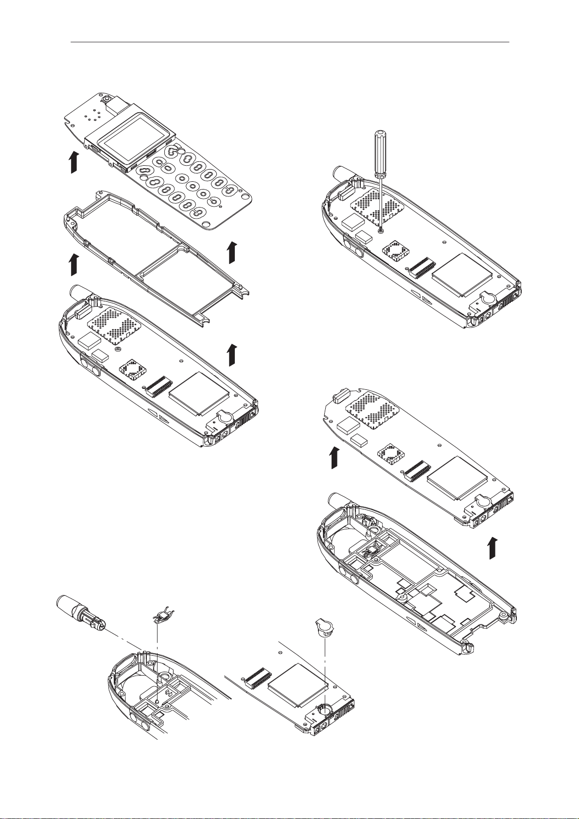
Disassembly 3. . . . . . . . . . . . . . . . . . . . . . . . . . . . . . . . . . . . . . . . .
Trouble Shooting 5. . . . . . . . . . . . . . . . . . . . . . . . . . . . . . . . . . . . .
Phone is totally dead 6. . . . . . . . . . . . . . . . . . . . . . . . . . . . . . . . . .
Flash programming doesn’t work 6. . . . . . . . . . . . . . . . . . . . . . .
Flash Programming (1) 8. . . . . . . . . . . . . . . . . . . . . . . . . . . . .
Flash Programming failure (2) 9. . . . . . . . . . . . . . . . . . . . . . .
Flash Programming failure (3) 10. . . . . . . . . . . . . . . . . . . . . . .
Flash Programming failure (4) 11. . . . . . . . . . . . . . . . . . . . . . .
Power doesn’t stay on, or phone is jammed 12. . . . . . . . . . . . . .
Display Information: Contact Service 13. . . . . . . . . . . . . . . . . . . .
The phone doesn’t register to the network or phone doesn’t make a call 13
Phone register failure 15. . . . . . . . . . . . . . . . . . . . . . . . . . . . . . .
SIM card is out of order 16. . . . . . . . . . . . . . . . . . . . . . . . . . . . . . .
SIM Card failure 17. . . . . . . . . . . . . . . . . . . . . . . . . . . . . . . . . . .
Audio failure (1) 18. . . . . . . . . . . . . . . . . . . . . . . . . . . . . . . . . . . .
Audio failure (2) 19. . . . . . . . . . . . . . . . . . . . . . . . . . . . . . . . . . . .
Charger failure 20. . . . . . . . . . . . . . . . . . . . . . . . . . . . . . . . . . . .
Receiver Fault (1) 21. . . . . . . . . . . . . . . . . . . . . . . . . . . . . . . . . .
Receiver Fault (2) 22. . . . . . . . . . . . . . . . . . . . . . . . . . . . . . . . . .
Receiver Fault (3) 23. . . . . . . . . . . . . . . . . . . . . . . . . . . . . . . . . .
Receiver Fault (4) 24. . . . . . . . . . . . . . . . . . . . . . . . . . . . . . . . . .
Receiver Fault (5) 25. . . . . . . . . . . . . . . . . . . . . . . . . . . . . . . . . .
Receiver Fault (6) 26. . . . . . . . . . . . . . . . . . . . . . . . . . . . . . . . . .
Receiver Fault (7) 27. . . . . . . . . . . . . . . . . . . . . . . . . . . . . . . . . .
Transmitter Fault (1) 28. . . . . . . . . . . . . . . . . . . . . . . . . . . . . . . .
Transmitter Fault (2) 29. . . . . . . . . . . . . . . . . . . . . . . . . . . . . . . .
Transmitter Fault (3) 30. . . . . . . . . . . . . . . . . . . . . . . . . . . . . . . .
Appendix A 31. . . . . . . . . . . . . . . . . . . . . . . . . . . . . . . . . . . . . . . .
Appendix B 32. . . . . . . . . . . . . . . . . . . . . . . . . . . . . . . . . . . . . . . .
Appendix C 33. . . . . . . . . . . . . . . . . . . . . . . . . . . . . . . . . . . . . . . .
Appendix D 34. . . . . . . . . . . . . . . . . . . . . . . . . . . . . . . . . . . . . . . .

PAMS
Technical Documentation NSE–3
Disassembly & Troubleshooting Instructions
Page 3
Original, 11/97
Remove battery
Remove dust cap
Remove back cover
screws (4 pcs)
Turn around.
Remove UI module
screws (2 pcs)
Carefully remove
A–cover
Note snap fixings !

PAMS
Technical Documentation
NSE–3
Disassembly & Troubleshooting Instructions
Page 4 Original, 11/97
Remove UI–module
and frame
Remove engine
module screw
(1 pcs)
Remove engine
module
Remove
RTC–battery
Pull out
antenna
Remove
microphone

PAMS
Technical Documentation NSE–3
Disassembly & Troubleshooting Instructions
Page 5
Original, 11/97
Trouble Shooting
The following hints should facility finding the cause of the problem when
the circuitry seems to be faulty. This trouble shooting instruction is di-
vided following section.
1. Phone is totally dead
2. Flash programming doesn‘t work
3. Power doesn‘t stay on or the phone is jammed
4. Display information: Contact Service
5. Phone doesn‘t register to the network or phone doesn‘t make a call.
6. Plug in SIM card is out of order ( insert SIM card or card rejected).
7. Audio fault.
8. Charging fault
The first thing to do is carry out a through visual check of the module. En-
sure in particular that:
a) there are not any mechanical damages
b) soldered joints are OK

PAMS
Technical Documentation
NSE–3
Disassembly & Troubleshooting Instructions
Page 6 Original, 11/97
Phone is totally dead
This means that phone doesn’t take current at all when the power switch
is pressed or when the watchdog disable pin (X001 pin 11) is grounded.
Used battery voltage must be higher than 3.0 V. Otherwise the hardware
of CCONT (N100) prevents totally to switch power on.
Phone is totally dead
YES
Check R118, X300
J232
VBAT is 3.6 V NO Failure in VBAT line
Check X101, X102, L103
YES
Voltage at pin 29 of CCONT (N100)
is 3.6 V
NO Faulty circuit N100
YES
N100 pin 55 (VBB) 2.8 V
N100 pin 25 (VXO) 2.8 V
when PWR switch is pressed
or watchdog disable pin is grounded
NO CCONT (N100) pin 29 0V when
PWR switch is pressed or
watchdog disable pin is (X001)
grounded
YES
See section: Power Doesn’t Stay On
YES
Faulty circuit N100
NO Check UI module
Check watchdog disable line to
X001
Flash programming doesn’t work
The flash programming can be done via panel connector X001 or via sys-
tem connector X100.
In production, the first programming is done via panel connector X001.
After this, the panel connector is cut away, thus other flash programmings
must be done via system connector X100.
The main differences between these are:
a) FLASH programming voltage is produced different way.
b) Signal routings are different.
The fault finding diagrams for flash programming via panel connector are
shown in figures 32 and 33.
The fault finding diagrams for flash programming via system connoctor
are shown in figures 34 and 35.
In flash programming error cases the flash prommer can give some in-
formation about a fault.

PAMS
Technical Documentation NSE–3
Disassembly & Troubleshooting Instructions
Page 7
Original, 11/97
The fault information messages could be:
– MCU doesn’t boot
– Serial clock line failure
– Serial data line failure
– External RAM fault
– Algorithm file or alias ID don’t find
– MCU flash Vpp error
In cases that the flash programming doesn’t succeed there is a possibility
to check short circuits between the memories and the MCU (MAD2).
This test is useful to do, when the fault information is: MCU doesn’t boot,
Serial clock line failure or Serial data line failure.
The test procedure is following:
1. Connect the short circuit wire between the test points J229 and J230.
2. Switch power on
3. If the voltage level in testpoint J225 is 2.8 V (”1”), the interface is OK. If
there is a short circuit, the voltage level in testpoint J225 stays low and
32kHz square wave signal can be seen in the lines which are al-
ready tested.
One must be noticed that this test can be found only short circuits, not
open pins.
Also upper data lines (15:8) of flash circuit D210 are not included to this
test.
CCONT pin 54( PURX )
MAD pin 38 ( MCUAD0)
MAD pin 134 ( ExtSysResX))selftest
passed J225

PAMS
Technical Documentation
NSE–3
Disassembly & Troubleshooting Instructions
Page 8 Original, 11/97
Flash Programming (1)
Flash programming doesn’t work
EEPROM (D240) pin 8 (VBB) 2.8 V
J522 (VXO) 2.8 V NO
See section: Phone is totally dead
YES
J227 master reset (Purx) = ”1” (2.8 V) NO J228 sleep clock(SCLK)
square wave 32 kHz NO
YES
Faulty circuit N100
or over loaded PurX line
check sleep
clock circuitry
(B100, R154...)
YES
MAD2 (D200) pin 93: 13 MHz sine wave
clock signal: 500 mVpp min.
YES
NO
J506 (RFC) 13 MHz
800 mV min
YES
check C213, R213
NO
check buffer V705 and
VCXO G600 Check that following lines are correct:
YES
If the fault information from the prommer is:
b) serial data line failure
a) MCU doesn’t boot
c) serial clock line failure
connect:
FCLK (MBUS) line: X001 pin 2 –> D200 pin 112
FTX (fbus_tx) line: X001 pin 1 –> D200 pin 104
FRX (fbus_rx) line: X001 pin 2 –> D200 pin 109
check also pullup and pulldown resistors: R203, R201, R215
OK
WDDIS line: X001 pin 11 –> N100 pin 29
GND : X001 pin 7 –> GND
connect watchdog disable (WDDIS) line (X001 pin 11) to the ground
check
OK
OK
Enable the selftest function of D200 by connecting
shortcircuit between testpoints J229 and J230
Connect an oscilloscope to testpoint J225 and switch
power on
Voltage level rises to ”1” after power on at testpoint J225 NO
YES
There is a shortcircuit
somewhere in memory control
lines or MCU address lines or
MCU lower (7:0) data lines
There could be open pins in circuits D200 (D211, D240)
If not, the PCB or D200 (D211, D240) is faulty

PAMS
Technical Documentation NSE–3
Disassembly & Troubleshooting Instructions
Page 9
Original, 11/97
Flash Programming failure (2)
Flash progrmming doesn’t work
YES
Faulty component D210
If the fault information from the prommer is:
External RAM fault
YES
Check pins of SRAM (D220)
Check control lines of SRAM:
RAMSelX ...
Flash progrmming doesn’t work
YES
If the fault information from the prommer is:
Algorithm file or alias ID don’t find, ID is un-
known etc.
YES
Check control lines and upper data lines (15:8)
of FLASH: ROM1SelX...
Check pins of FLASH (D210)
Flash progrmming doesn’t work
YES
If the fault information from the prommer is:
MCU flash Vpp error
YES
Check connection between X001; 10 ––> D210; 13
Check components C212, R211
OK

PAMS
Technical Documentation
NSE–3
Disassembly & Troubleshooting Instructions
Page 10 Original, 11/97
Flash Programming failure (3)
Flash programming doesn’t work
EEPROM (D240) pin 8 (VBB) 2.8 V
J522 (VXO) 2.8 V NO
YES
J227 master reset (Purx) = ”1” (2.8 V) NO J228 sleep clock(SCLK)
square wave 32 kHz NO
YES
Faulty circuit N100
or over loaded PurX line
check sleep
clock circuitry
(B100, R154...)
YES
MAD2 (D200) pin 93: 13 MHz sine wave
clock signal: 500 mVpp min.
YES
NO
J506 (RFC) 13 MHz
800 mV min
YES
check C213, R213
NO
check buffer V705 and
VCXO G600 Check that following lines are correct:
YES
If the fault information from the prommer is:
b) serial data line failure
a) MCU doesn’t boot
c) serial clock line failure
connect:
FCLK (MBUS) line: X100 pin 11 –> D200 pin 112
FTX (fbus_tx) line: X100 pin 13 –> D200 pin 104
FRX (fbus_rx) line: X100 pin 12 –> D200 pin 109
check also pullup and pulldown resistors: R203, R201, R215
OK
GND : X100 pin 14 –> GND
connect the shortcircuit fire from N100 pin 29 to ground (watchdog)
N100 is faulty
OK
Enable the selftest function of D200 by connecting
shortcircuit between testpoints J229 and J230
Connect an oscilloscope to testpoint J225 and switch
power on
Voltage level rises to ”1” after power on at testpoint J225 NO
YES
There is a shortcircuit
somewhere in memory control
lines or MCU address lines or
MCU lower (7:0) data lines
There could be open pins in circuits D200 (D211, D240)
If not, the PCB or D200 (D211, D240) is faulty
VBAT is correct
3.6 V
YES

PAMS
Technical Documentation NSE–3
Disassembly & Troubleshooting Instructions
Page 11
Original, 11/97
Flash Programming failure (4)
Flash progrmming doesn’t work
YES
Faulty component D210
If the fault information from the prommer is:
External RAM fault
YES
Check pins of SRAM (D220)
Check control lines of SRAM:
RAMSelX ...
Flash progrmming doesn’t work
YES
If the fault information from the prommer is:
Algorithm file or alias ID don’t find, ID is un-
known etc.
YES
Check control lines and upper data lines (15:8)
of FLASH: ROM1SelX...
Check pins of FLASH (D210)
Flash progrmming doesn’t work
YES
If the fault information from the prommer is:
MCU flash Vpp error
YES
Vpp > 4.5 V in D210 pin 13 (or C212)
Check components C212, R211
YES
NO Vpp > 4.5 V in testpoint J221
YES
NO
Check UI connector X300
Check regulator N201
OK

PAMS
Technical Documentation
NSE–3
Disassembly & Troubleshooting Instructions
Page 12 Original, 11/97
Power doesn’t stay on, or phone is jammed
If this kind of fault has come after flash programming, there are most
probably open pins in ICs.
The soldered joints of ICs: D200 (MAD2), D210 (FLASH), N100
(CCONT), D221 (SRAM) are useful to check at first.
Normally the power will be switched of by CCONT (N100) after 30 se-
conds, if the watchdog of the CCONT can not be served by software.
The watchdog updating can be seen by oscilloscope at pin 50 (DataselX)
of CCONT.
In normal case there is a short pulse from ”1” –> 0 every 8 seconds.
The power off function of CCONT can be prevented by connecting a short
circuit wire from CCONT pin 29 to ground.
Power doesn’t stay on or phone is jammed
EEPROM (D240) pin 8 (VBB) 2.8 V
J522 (VXO) 2.8 V NO
YES
J227 master reset (Purx) = ”1” (2.8 V) NO J228 sleep clock(SCLK)
square wave 32 kHz NO
YES
Faulty circuit N100
or over loaded PurX line
check sleep
clock circuitry
(B100, R154...)
YES
MAD2 (D200) pin 93: 13 MHz sine wave
clock signal: 500 mVpp min.
YES
NO
J506 (RFC) 13 MHz
800 mV min
YES
check C213, R213
NO
check buffer V705 and
VCXO G600
YES
connect the shortcircuit fire from N100 pin 29 to ground (watchdog)
N100 is faulty
OK
VBAT is correct
3.6 V
YES
CCONT watchdog is served?
(pin 50 pulses 1 –> 0)
NO
YES
software is able to run
check UI module
after few seconds, check
BSI and BTEM lines
If power is switched off
Open pins or faulty circuit:
D200, D210, D221, N100
R215

PAMS
Technical Documentation NSE–3
Disassembly & Troubleshooting Instructions
Page 13
Original, 11/97
Display Information: Contact Service
This fault means that software is able to run and thus the watchog of
CCONT (N100) can be served.
Selftest functions are run when power is switched on and software is
started to excute from flash.
If any of selftests is failed, contact service information will be shown on
display.
The phone doesn’t register to the network or phone
doesn’t make a call
If the phone doesn’t register to the network or the phone doesn’t make a
call, the reason could be either the baseband or the RF part.
The phone can be set to wanted mode by WinTesla service software and
determinate if the fault is in RF or in baseband part (RF interface mea-
surements).
The control lines for RF part are supplied both the System Asic
(MAD2;D200) and the RFI (Cobba; N250). MAD2 handles digital control
lines ( like synthe, TxP etc.) and Cobba handles analog control lines (like
AFC, TxC etc.).
The DSP software is constructed so that operation states of DSP (MAD2)
can be seen in external flag (DSPXF) output pin (D200 pin 91).
After power up, DSP signals all completed functions by changing the state
of the XF pin (see figures 39 and 40).
MAD2 pin 91 (DSPXF)
1 2 3
1. DSP initialization done
2.Synchronization to network
done
3. Registrarition to network
done.
J222

PAMS
Technical Documentation
NSE–3
Disassembly & Troubleshooting Instructions
Page 14 Original, 11/97
1
2
3
MAD2 pin 91 (DSPXF)
J222
MAD2 pin 91 (DSPXF)
J222
MAD2 pin 91 (DSPXF)
J222
init
initialize patch code
download
dsp
constants
download
initialization
done
synchronization
OK
channel
scan starts
PSW
search last PSW
OK
send RACH
RACH OK
go SDCCH
imediate assigment
OK

PAMS
Technical Documentation NSE–3
Disassembly & Troubleshooting Instructions
Page 15
Original, 11/97
Phone register failure
Phone doesn’t register to the network
or
phone doesn,t make a call
YES
Analog supply voltage VCOBBA is >2.7 V
at pin 7,12 ... of Cobba (N250)
NO
YES
Check
N100
Analog reference voltage Vref is 1.5 V
at pin 9 of Cobba (N250)
NO Check
R270, R271
YES
Supply voltage VCP (N100 pin 32) > 4.8 V
Supply voltage VRX (N100 pin 9) > 2.7 V
Supply voltage VSYN_1 (N100 pin 15) > 2.7 V
Supply voltage VSYN_2 (N100 pin 4) > 2.7 V
during the receiving slot
Supply voltage VTX (N100 pins 11, 20) > 2.7 V
during the transmitting slot
YES
NO Check
N100, D200
Synthesizer lines: SEna (N620 pin 56),
SClk (N620 pin 54)
SData (N620 pin 55)
pulses 0 –> 1 during receiving slot
NO Check
D200
YES
RF control lines: RxC (N250 pin 18) 0 –> 2.3 Vmax during receiving slot
AFC (N250 pin 19) 0 – 1.2 V typ. during receiving slot
NO Check
N250
YES
Analog data signal RxIP (N250 pin 22) 0–> 1.5 V DC during receiving slot
Analog data signal RxIN (N250 pin 22) 0–> 1.5 V DC during receiving slot
Used benefit signal is biased to DC and its amplitude is 50 mVpp
nominal and frequency is 13 MHz
NO Check
N250 if DC is failed
Check
RF part if benefit signal is failed
YES
DAX signal (N250 pin 48) pulses 1 –> 0 during receiving slot NO Check
N250
RF control lines: TxC (N250 pin 17) 0 –> 2.3 Vmax during transmit slot
TxP (D200 pin 176) 0–>1 (2.8 V) during transmit slot
YES Check
N250 if TxC is failed
Check
D200 if TxP is failed
NO
YES
Analog data signals: TxIN (N250 pin 13) 0–> 0.8 V DC during transmit slot
TxIP (N250 pin 14) 0 –>0.8 V DC during transmit slot
TxQN (N250 pin 15) 0 –>0.8 V DC during transmit slot
TxQP (N250 pin 16) 0 –>0.8 V DC during transmit slot
Used benefit signal is biased to DC and its amplitude is 300 mVpp
nominal and frequency is 64 kHz
NO Check
N250
YES Check
RF part

PAMS
Technical Documentation
NSE–3
Disassembly & Troubleshooting Instructions
Page 16 Original, 11/97
SIM card is out of order
The hardware of the SIM interface from MAD2 (D200) to the SIM connec-
tor (X302) can be tested without SIM card.
When the power is switched on and if the BSI line (X101;1) is grounded
by resistor, all the used lines (VSIM, RST, CLK, DATA) rises up to 5 V four
times. Thus ”Insert SIM card” faults can be found without SIM card.
The fault information ”Card rejected” means that ATR message (the first
message is always sent from card to phone) is sent from card to phone
but the message is somehow corrupted, data signal levels are wrong etc.
or factory set values (stored to the EEPROM) are not correct.

PAMS
Technical Documentation NSE–3
Disassembly & Troubleshooting Instructions
Page 17
Original, 11/97
SIM Card failure
Insert SIM card fault
Voltage level < 1.5 V
at pin 95 of D200 when
YES
NO Check
R120, R122, X101
C120, C160
YES
BSI resistor is connected
VSIM, DATA, RESET and CLOCK lines
rises up to 5 V after power on at pins
of SIM card
NO
YES Check
SIM card and SIM reader
connectors
VSIM(36), DATAO(43),SIMRSTO(42) and SIMCLKO(38) lines
rises up to 5 V after power on at pins of N100 (CCONT)
NO
YES Check
X302, R124, R125, R128
SIMPWR(30), DATAA(44), SIMRSTA(40), SIMCLK(41) and SIMIOC(39) lines
rises up to 2.8 V after power on at pins of N100 (CCONT) YES faulty circuit
N100 (CCONT)
NO
SIMCardPwr(129), SIMCardData(120), SIMCardRstX(127), SIMCardClk(126) and SIMCardIOC(128) lines
rises up to 2.8 V after power on at pins of D200 (MAD2)
NO
YES faulty PCB
Check again that voltage level at pin 95 (SIMCardDetX) of D200 is lower than 1.5V
If it is, change D200
Card Rejected fault
YES
VSIM is according the specification
VSIM = 2.8 V min (with 3 V SIM card)
VSIM = 4.5 V min (with 5 V SIM card)
NO faulty circuit
N100 (CCONT)
YES
The ATR data can be seen at pin 43
(CCONT, N100)
NO Check
X302, R124
YES
The ATR data can be seen at pin 120
(MAD2, D200) NO Check
N100
YES
SIMIOControl line (N100 pin 36) is ”1”
during the ATR message
NO Check
D200
YES
Check D200

PAMS
Technical Documentation
NSE–3
Disassembly & Troubleshooting Instructions
Page 18 Original, 11/97
Audio failure (1)
Uplink (microphone) and downlink (earphone) are broken
Voltage at pin 107 of MAD2 (D200)
is 2.8 V (without external audio de-
vices) HOOKDET
NO
YES
Check
R259, R260
Voltage at pin 108 of MAD2 (D200)
is 2.8 V (without external audio de-
vices) HEADDET
NO Check
R257, R256, R261
YES
Frequency at pin 138 of MAD2 (D200)
is 1 MHz, square wave 2.8 Vpp
NO Check
N250 (Cobba)
Frequency at pin 139 of MAD2 (D200)
is 8 kHz, square wave pulses 2.8 Vpp
YES
NO Check
N250 (Cobba)
Uplink (microphone) is broken
Voltage at pin 6 of X100 is 1.8 V
Voltage at pin 7 of X100 is 0.3 V NO
YES Check
microphone, X100 and micbias
components V250...
If OK, check that micbias control line
is (D200 pin1 ) 2.8 V during a call
during a call
YES
DC voltage at pins 59 and 60 of
N250 is 1.4 V during a call
NO Check
N250 (Cobba)
YES
Analog audio signal (few millivolts) at pins 59 and 60
of N250 during a call NO Check
C262, C263 and PCB
routings
YES
Check
N250 (Cobba)
Digital PCM data at pin 137 of MAD2 (D200)
during a call NO
YES

PAMS
Technical Documentation NSE–3
Disassembly & Troubleshooting Instructions
Page 19
Original, 11/97
Audio failure (2)
Check
D200 (MAD2)
Digital PCM data at pin 52 of Cobba (N250)
during a call NO
Downlink (earphone) is broken
YES
YES
DC voltage at pins 5 and 6 of
N250 is 1.4 V during a call
NO Check
N250 (Cobba)
YES
Analog audio signal (some ten millivolts) at pins 5 and
6 of N250 during a call
NO Check
N250 (Cobba)

PAMS
Technical Documentation
NSE–3
Disassembly & Troubleshooting Instructions
Page 20 Original, 11/97
Charger failure
YES
Nothing happens when charger is connected
Voltage level at pin 60 of CCONT (N100)
is higher than 0.4 V when charger is con-
nected
NO Check
X100, F100, L104
R104, R103
YES
Check N100
Display Information: Not charging
YES
Voltage level at pin 62 of CCONT (N100)
is about 0.8 V when power is connected
BSI resistor value should be 39 k
NO Check
X101, R120, R122
YES
Voltage level at pin 63 of CCONT (N100)
is about 0.5 V when power is connected
BTEMP resistor value should be 47 k
NO Check
X101, R120, R122
YES
32 Hz square wave frequency at pin 7 of CHAPS (N101) NO Check
N100
Check
N101
YES
Voltage levels at pins 5 and 12 of CHAPS (N101)
are same as VB
NO Check
R131, N101
YES
Voltage levels at pins 5 and 12 of CHAPS (N101)
rises when charger is connected
NO
Other manuals for 6110 - Navigator Smartphone 40 MB
5
Table of contents
Other Nokia Cell Phone manuals