Nokia NPL-4 Series Guide

Nokia Customer Care
NPL-4/5/RM-104 Series Transceivers
Issue 2 05/05 Copyright © 2005 Nokia Corporation. All rights reserved.
Troubleshooting Instructions

NPL-4/5/RM-104 Companyconfidential
Troubleshooting Instructions Nokia Customer Care
Page 2 Copyright © 2005 Nokia Corporation. All rights reserved. Issue 2 05/05
[This page left intentionally blank]

Nokia Customer Care Troubleshooting Instructions
Company confidential NPL-4/5/
Issue 2 05/05 Copyright © 2005 Nokia Corporation. All rights reserved. Page 3
Table of Contents
Page No
RF Troubleshooting ....................................................................................................... 7
Introduction to RF troubleshooting .............................................................................7
RF Key component placement .....................................................................................8
RF Test Points................................................................................................................ 9
Receiver .....................................................................................................................10
Transmitter .................................................................................................................11
Synthesizer .................................................................................................................11
RF in General............................................................................................................... 12
RF Power Supply Configuration.................................................................................. 14
Receiver Verification and Troubleshooting................................................................. 16
General instructions for RX troubleshooting .............................................................16
Measuring RX I/Q Signals using RSSI Reading..................................................... 16
Measuring RX performance using SNR measurement ........................................... 18
Measuring front-end power levels using spectrum analyzer................................... 19
Measuring analogue RX I/Q signals using oscilloscope......................................... 20
Fault finding chart of the receiver........................................................................... 21
Rx signal paths ...........................................................................................................25
Antenna switch (RX/TX switch)............................................................................. 25
Rx front-end ............................................................................................................ 26
RX paths of RF ASIC.............................................................................................. 27
Transmitter................................................................................................................... 28
General instructions for transmitter troubleshooting .................................................28
Transmitter troubleshooting .......................................................................................28
Antenna switch (TX/RX switch)............................................................................. 28
GSM850 transmitter ..................................................................................................29
General instructions for GSM850 TX troubleshooting........................................... 29
GMSK ..................................................................................................................... 29
EDGE...................................................................................................................... 30
Fault Finding Chart for GSM850 Transmitter ........................................................ 32
GMSK ..................................................................................................................... 33
EDGE...................................................................................................................... 34
GSM900 transmitter ..................................................................................................34
General instructions for GSM TX troubleshooting................................................. 34
GMSK ..................................................................................................................... 34
EDGE...................................................................................................................... 35
Fault finding chart for GSM900 transmitter ........................................................... 36
GMSK ..................................................................................................................... 37
EDGE...................................................................................................................... 38
GSM1800 transmitter ................................................................................................38
General instructions for GSM1800 TX troubleshooting......................................... 38
GMSK ..................................................................................................................... 38
EDGE...................................................................................................................... 39
Fault finding chart for GSM1800 transmitter ......................................................... 40
GMSK ..................................................................................................................... 41
EDGE...................................................................................................................... 42
GSM1900 transmitter ................................................................................................42
General instructions for GSM1900 TX troubleshooting......................................... 42

NPL-4/5/RM-104 Companyconfidential
Troubleshooting Instructions Nokia Customer Care
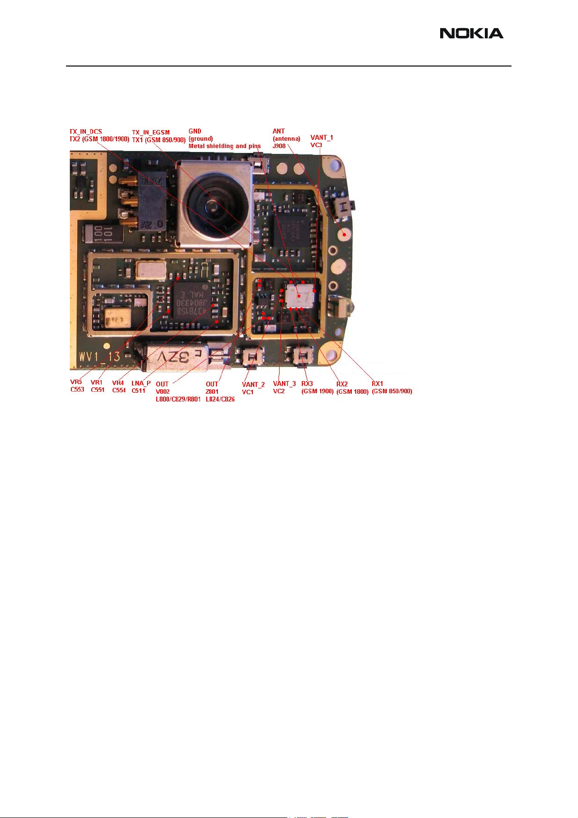
Page 4 Copyright © 2005 Nokia Corporation. All rights reserved. Issue 2 05/05
GMSK ..................................................................................................................... 42
EDGE...................................................................................................................... 43
Fault finding chart for GSM1900 transmitter ......................................................... 44
GMSK ..................................................................................................................... 45
EDGE...................................................................................................................... 46
Synthesizer................................................................................................................... 47
Check synthesizer operation ......................................................................................47
Reference oscillator 26 MHz (VCTCXO) .................................................................48
Voltage Controlled Oscillator (VCO) ........................................................................49
Fault finding chart for PLL synthesizer .....................................................................50
Pictures of synthesizer signals ...................................................................................51
Frequency tables ........................................................................................................53
GSM850.................................................................................................................. 53
GSM900 (including EGSM900) ............................................................................. 54
GSM1800................................................................................................................ 55
GSM1900................................................................................................................ 57
DC Supply Current Check ........................................................................................... 59
Baseband Troubleshooting........................................................................................... 60
BB measurement points .............................................................................................60
Troubleshooting diagrams .........................................................................................62
Phone is dead. ............................................................................................................63
Phone is jammed 1 .....................................................................................................64
Phone is jammed 2 .....................................................................................................65
Flash faults 1 ..............................................................................................................66
Flash faults 2 ..............................................................................................................67
SIM card faults ..........................................................................................................68
Charger faults .............................................................................................................69
Display faults 1 ..........................................................................................................70
Display faults 2 ..........................................................................................................71
Audio fault1 ...............................................................................................................72
Audio fault 2 ..............................................................................................................73
Audio fault 3 ..............................................................................................................74
Keyboard faults 1 .......................................................................................................75
Keyboard faults 2 .......................................................................................................76
Keyboard faults 3 .......................................................................................................77
Keyboard faults 4 .......................................................................................................78
Keyboard faults 5 .......................................................................................................79
Accessory faults1 .......................................................................................................80
Accessory faults 2 ......................................................................................................82
Flashlight faults .........................................................................................................84
Self tests .....................................................................................................................85
FCI troubleshooting ...................................................................................................86
IHF troubleshooting ...................................................................................................88
Compass Troubleshooting............................................................................................ 89
Calibration 1 ..............................................................................................................90
Calibration 2 ..............................................................................................................91
Sensor problems 1 ......................................................................................................92
Start calibration ..........................................................................................................93

Nokia Customer Care Troubleshooting Instructions
Company confidential NPL-4/5/
Issue 2 05/05 Copyright © 2005 Nokia Corporation. All rights reserved. Page 5
Magic troubleshooting ...............................................................................................96
FM Radio Troubleshooting.......................................................................................... 97
FM radio component layout .......................................................................................97
FM radio troubleshooting diagram ............................................................................99
Notes to "FM radio troubleshooting diagram"........................................................ 99
List of Figures
Page No
Fig 1 Component placement 1.............................................................................................8
Fig 2 Picture of the Assembled PWB with Chambers.........................................................9
Fig 3 Receiver Test Points...................................................................................................10
Fig 4 Transmitter Test Points...............................................................................................11
Fig 5 Synthesizer Test Points...............................................................................................11
Fig 6 RF Block -Diagram ....................................................................................................12
Fig 7 RF Power Supply Configuration ................................................................................13
Fig 8 RSSI Window.............................................................................................................17
Fig 9 Signal Measurement...................................................................................................19
Fig 10 Signal Amplitudes ....................................................................................................20
Fig 11 RX IQ Signals...........................................................................................................21
Fig 12 Receiver Fault Chart 1..............................................................................................22
Fig 13 Receiver Fault Chart 2..............................................................................................23
Fig 14 Receiver Fault Chart 3, 4, 5 .....................................................................................23
Fig 15 Receiver Fault Chart 6..............................................................................................24
Fig 16 Receiver Fault Chart 7..............................................................................................24
Fig 17 Receiver Fault Chart 8..............................................................................................25
Fig 18 Receiver Fault Chart 9..............................................................................................25
Fig 19 Block Diagram of Antenna Switch: Left Input Port (Antenna) and Right Output Ports
Rx/Tx .....................................................................................................................................26
Fig 20 RF Controls ..............................................................................................................30
Fig 21 RF Controls ..............................................................................................................32
Fig 22 Band Selection..........................................................................................................35
Fig 23 RF Control Values....................................................................................................36
Fig 24 RF Control Values....................................................................................................39
Fig 25 RF Control Values....................................................................................................40
Fig 26 RF Control Values....................................................................................................43
Fig 27 RF Control Values....................................................................................................44
Fig 28 Typical Feature Tuning Curve for the Matshushita VCO........................................48
Fig 29 26 Mhz at G501 Pin Out...........................................................................................51
Fig 30 26 MHz RFCLK at R420/C420................................................................................51
Fig 31 VCO Output, 1800 Band, RX on, Continuous Output.............................................52
Fig 32 DC Power Supply Diagram......................................................................................59
Fig 33 NPL-4/5 BB Measurement Points, Top ...................................................................60
Fig 34 NPL-4/5 BB Measurement Points, Bottom..............................................................61
Fig 35 MBUS.......................................................................................................................81
Fig 36 ACI Diagram ...........................................................................................................83
Fig 37 Testpoints .................................................................................................................94
Fig 38 Component placement .............................................................................................97
Fig 39 Trace layout.............................................................................................................98

NPL-4/5/RM-104 Companyconfidential
Troubleshooting Instructions Nokia Customer Care
Page 6 Copyright © 2005 Nokia Corporation. All rights reserved. Issue 2 05/05
Fig 40 FM radio block layout. .............................................................................................98
Fig 41 FM radio troubleshooting diagram...........................................................................100
Fig 42 Oscilloscope screen shot, Audio output ...................................................................101
Fig 43 FM radio clock from test point J359, 32 kHz frequency clock signal, when radio is on.
102
Fig 44 FM frequency from FM radio pin 37, the other end of L358, with FM test signal..102
Fig 45 VCO frequency from FM radio pins 3 and 4, the other ends of V356 and V357, with
FM test signal.........................................................................................................................102

Nokia Customer Care Troubleshooting Instructions
Company confidential NPL-4/5/
Issue 2 05/05 Copyright © 2005 Nokia Corporation. All rights reserved. Page 7
RF Troubleshooting
Introduction to RF troubleshooting
Measurements should be done using Spectrum analyzer with high-frequency high-
impedance passive probe (LO-/reference frequencies and RF power levels) and Oscillo-
scope with a 10:1 probe (DC-voltages and low frequency signals)
The RF-section is built around one RF-ASIC (Helgo N500). For easier troubleshooting, this
RF troubleshooting document is divided in to sections.
Before changing Helgo, please check following things: Supply voltages are OK and serial
communication is coming from baseband to Helgo.
Please note that the grounding of the PA module is directly below PA-module so it is dif-
ficult to check or change. Most RF semiconductors are static discharge sensitive! So
ESD protection must be taken care of during repair (ground straps and ESD soldering
irons). Helgo and PA are moisture sensitive so parts must be pre-baked prior to soldering.
Apart from key components described in this document here are a lot of discrete compo-
nents (resistors, inductors and capacitors) which troubleshooting is done by checking if
soldering of the component is done properly (for factory repairs checking if it is missing
from PWB). Capacitor can be checked for shortening and resistors for value by means of
an ohmmeter, but be aware in-circuit measurements should be evaluated carefully.
Please be aware that all measured voltages or RF levels in this document are rough fig-
ures. Especially RF levels varies due to different measuring equipment or different
grounding of the used probe. When using RF probe usually a good way is to use metallic
tweezers to connect probe ground to PWB ground as close to measurement point as pos-
sible.

NPL-4/5/RM-104 Companyconfidential
Troubleshooting Instructions Nokia Customer Care
Page 8 Copyright © 2005 Nokia Corporation. All rights reserved. Issue 2 05/05
RF Key component placement
Figure 1: Component placement 1

Nokia Customer Care Troubleshooting Instructions
Company confidential NPL-4/5/
Issue 2 05/05 Copyright © 2005 Nokia Corporation. All rights reserved. Page 9
RF Test Points
The RF power supplies are generated in the UEM and can be measured either in the Small
Signal Chamber or in the Baseband Chamber. On the drawings below small points show
the locations of the test points.
Figure 2: Picture of the Assembled PWB with Chambers

NPL-4/5/RM-104 Companyconfidential
Troubleshooting Instructions Nokia Customer Care
Page 10 Copyright © 2005 Nokia Corporation. All rights reserved. Issue 2 05/05
Receiver
Figure 3: Receiver Test Points

Nokia Customer Care Troubleshooting Instructions
Company confidential NPL-4/5/
Issue 2 05/05 Copyright © 2005 Nokia Corporation. All rights reserved. Page 11
Transmitter
Figure 4: Transmitter Test Points
Synthesizer
Figure 5: Synthesizer Test Points

NPL-4/5/RM-104 Companyconfidential
Troubleshooting Instructions Nokia Customer Care
Page 12 Copyright © 2005 Nokia Corporation. All rights reserved. Issue 2 05/05
RF in General
Figure 6: RF Block -Diagram
RF block diagram consisting of:
• RF front-end module
• Power amplifier module
•RFASIC
• VCTCXO module
• VCO module

Nokia Customer Care Troubleshooting Instructions
Company confidential NPL-4/5/
Issue 2 05/05 Copyright © 2005 Nokia Corporation. All rights reserved. Page 13
The RF front-end is a triple-band direct conversion transceiver. Using direct conversion,
no intermediate frequencies are used for up- or down-conversion.
Figure 7: RF Power Supply Configuration
GSM: 869-894 MHz
925-960 MHz
DCS: 1805-1880 MHz
PCS: 1930-1990 MHz
f
f
f/4
f/4 f
f
Helgo
f/2
f/2 PLL
3296-
3980
MHz
I-signal
Q-signal RX
I-signal
Q-signal TX
PCS: 1850-1910 MHz
DCS: 1710-1785 MHz
GSM: 824-849 MHz
880-915 MHz
Buffer VCTCXO
26 MHz
26 MHz
VCTCXO
AFC

NPL-4/5/RM-104 Companyconfidential
Troubleshooting Instructions Nokia Customer Care
Page 14 Copyright © 2005 Nokia Corporation. All rights reserved. Issue 2 05/05
RF Power Supply Configuration
General Specifications of Transceiver
Parameter Unit
Cellular System GSM850/900, GSM1800, GSM1900
Modulation schemes GMSK, 8-PSK
RX Frequency Band GSM850:824 … 849 MHz
GSM900:925 … 960 MHz
GSM1800:1805 ... 1880 MHz
GSM1900:1930 … 1990 MHz
TX Frequency Band GSM850:869 … 894 MHz
GSM900:880 … 915 MHz
GSM1800:1710 ... 1785 MHz
GSM1900:1850 … 1910 MHz
Output Power GMSK GSM850:+5 … +33 dBm (3.2 mW … 2 W)
GSM900:+5 … +33 dBm (3.2 mW … 2 W)
GSM1800:+0 … +30 dBm (1.0 mW … 1 W)
GSM1900:+0 … +30 dBm (1.0 mW … 1 W)
Output Power 8-PSK GSM850:+5 … 27 dBm (3.2 mW … 0.5 W)
GSM900:+5 … 27 dBm (3.2 mW … 0.5 W)
GSM1800:+0 … 26 dBm (1.0 mW … 0.4 W)
GSM1900:+0 … 26 dBm (1.0 mW … 0.4 W)
Duplex Spacing GSM850:45 MHz
GSM 900:45 MHz
GSM 1800:95 MHz
GSM 1900:80 MHz
Number of RF Channels GSM 850:124
GSM 900:174
GSM 1800:374
GSM1900:299
Channel Spacing 200 kHz (each band)
Number of TX Power Levels
GMSK
EGSM:15
GSM 900:15
GSM 1800:16
GSM 1900:16
Number of TX Power Levels
8-PSK
GSM 850:12
GSM 900:12
GSM 1800:14
GSM 1900:14
Sensitivity, static channel
(+25°C)
EGSM:-102 dBm
GSM 900:-102 dBm
GSM 1800:-102 dBm
GSM 1900:-102 dBm

Nokia Customer Care Troubleshooting Instructions
Company confidential NPL-4/5/
Issue 2 05/05 Copyright © 2005 Nokia Corporation. All rights reserved. Page 15
Frequency Error, static channel < 0.1 ppm
RMS Phase Error < 5.0 °
Peak Phase Error < 20.0 °

NPL-4/5/RM-104 Companyconfidential
Troubleshooting Instructions Nokia Customer Care
Page 16 Copyright © 2005 Nokia Corporation. All rights reserved. Issue 2 05/05
Receiver Verification and Troubleshooting
General instructions for RX troubleshooting
Connect the phone to a PC, which has Phoenix Service Software and a dongle installed,
using either
• Repair jig and DAU-9S (RS232) cable or
• DAU-9T cable (RS232) or
• DKU-5 cable (USB)
Connect the phone to a power supply (DC voltage: 4.0V, max. current: 3A) and an RF sig-
nal generator. Switch the phone on.
Start Phoenix Service Software and open FBUS connection.
- Select →Scan Product (Ctrl-R)
Wait until phone information (NPL-4 or NPL-5) is shown in the lower right corner of the
screen.
Follow the instructions below.
Measuring RX I/Q Signals using RSSI Reading
- Start Phoenix Service Software and open FBUS connection.
- Select →Scan Product (Ctrl-R)
Wait until phone information is shown in the lower right corner of the screen.
- Set operating mode to local mode
- Select →Testing →RF Controls
- Select →Band →GSM 850 or GSM 900 or GSM1800 or GSM1900
Active unit →RX
Operation mode →Burst
RX/TX Channel →190 or 37 or 700 or 661
- Select →Testing →RSSI reading
In the RSSI Reading window the “measuring mode” shall be set on Sum vector and the
“reading mode” on Continuous.

Nokia Customer Care Troubleshooting Instructions
Company confidential NPL-4/5/
Issue 2 05/05 Copyright © 2005 Nokia Corporation. All rights reserved. Page 17
The set up should now look like this:
Figure 8: RSSI Window
- Make the following settings on your signal generator:
Frequencies:
• GSM 850: 869.26771 MHz (channel 190 + 67.710 kHz offset)
• GSM 900: 942.46771 MHz (channel 37 + 67.710 kHz offset)
• GSM 1800: 1842.86771 MHz (channel 700 + 67.710 kHz offset)
• GSM 1900: 1960.06771 MHz (channel 661 + 67.710 kHz offset)
2. RF power level:
– 60 dBm @ the antenna connector of the phone/ test jig
(Remember to compensate for the cable and jig attenuation).
- Click on “Read now” in RSSI reading.
The resulting RSSI level shall be – 60 dBm +/– 0.5 dB in each band.

NPL-4/5/RM-104 Companyconfidential
Troubleshooting Instructions Nokia Customer Care
Page 18 Copyright © 2005 Nokia Corporation. All rights reserved. Issue 2 05/05
Measuring RX performance using SNR measurement
- Start Phoenix Service Software and open FBUS connection.
- Select →Scan Product (Ctrl-R)
Wait until phone information is shown in the lower right corner of the screen.
- Set operating mode to “local mode”.
- Select →Testing →RF Controls
- Select →Band →GSM 850 or GSM 900 or GSM1800 or GSM1900
Active unit →RX
Operation mode →Burst
RX/TX Channel →190 or 37 or 700 or 661
- Select →Testing →SNR Measurement
- Select →Measuring mode →Fast SNR (Radio Button)
- Press →Start
The window “Signal Measurement” pops up informing on frequency and power level of
the signal generator to be set.
- Press “ok” and the window will close.
- Read the SNR results.
The values should exceed:
• GSM 850: > 20 dB
• GSM 900: > 20 dB
• GSM 1800: > 18 dB
• GSM 1900: > 18 dB
The set up should now look like this:

Nokia Customer Care Troubleshooting Instructions
Company confidential NPL-4/5/
Issue 2 05/05 Copyright © 2005 Nokia Corporation. All rights reserved. Page 19
Figure 9: Signal Measurement
- Choose the remaining GSM bands and measure accordingly the procedure described
above.
Measuring front-end power levels using spectrum analyzer
Spectrum Analyzer (SA) level values depend on the probe type and shall be verified by a
properly working phone sample.
- Start Phoenix Service Software and open FBUS connection.
- Select →Scan Product (Ctrl-R)
Wait until phone information is shown in the lower right corner of the screen.
- Set operating mode to “local mode”
- Select →Testing →RF Controls
- Select →Band →GSM850 or GSM 900 or GSM1800 or GSM1900
Active unit →RX
Operation mode →Continuous
RX/TX Channel →190 or 37 or 700 or 661

NPL-4/5/RM-104 Companyconfidential
Troubleshooting Instructions Nokia Customer Care
Page 20 Copyright © 2005 Nokia Corporation. All rights reserved. Issue 2 05/05
Measuring analogue RX I/Q signals using oscilloscope
Measuring with an oscilloscope on “RXIINN”, (R421) or “RXQINN”, (R423) is recom-
mended only if RSSI reading does not provide enough information. Input level = -60dBm.
- Start Phoenix Service Software and open FBUS connection.
- Select →Scan Product (Ctrl-R)
Wait until phone information is shown in the lower right corner of the screen.
- Set operating mode to “local mode”
- Select →Testing →RF Controls
Wait until the RF Controls window is popped up.
- Select →Band →GSM 850 or GSM 900 or GSM1800 or GSM1900
Active unit →RX
Operation mode →continuous
RX/TX Channel →190 or 37 or 700 or 661
AGC →12
Following diagram should be displayed on an oscilloscope' s screen if the GSM 900
receiver is working properly:
Figure 10: Signal Amplitudes
Other manuals for NPL-4 Series
2
This manual suits for next models
2
Table of contents
Other Nokia Cell Phone manuals

Nokia
Nokia 3570 - Cell Phone - CDMA User manual

Nokia
Nokia 6720 classic User manual

Nokia
Nokia 9300 - Smartphone 80 MB User manual

Nokia
Nokia TA-1582 User manual

Nokia
Nokia N70 Music Edition User manual

Nokia
Nokia X3 User manual

Nokia
Nokia 1221 - Cell Phone - AMPS User manual

Nokia
Nokia N 80 User manual

Nokia
Nokia 2330 Classic User manual

Nokia
Nokia 6800 User manual