Nokia RH-13 Series Operating instructions

CCS Technical Documentation
RH-13 Series Transceivers
Issue 1 11/02 ãNokia Corporation
Troubleshooting

RH-13
Troubleshooting CCS Technical Documentation
Page 2 ãNokia Corporation Issue 1 11/02
Contents Page No
Transceiver Troubleshooting ......................................................................................... 5
General about testing ...................................................................................................5
Phone operating modes ............................................................................................. 5
Measurement points .....................................................................................................6
Baseband Troubleshooting............................................................................................. 8
Power up sequence ......................................................................................................8
Phone does not start up normally or does not stay on............................................. 11
Flash Programming does not work.......................................................................... 12
Flash programming error codes............................................................................... 14
Charging ....................................................................................................................16
Audio failures ............................................................................................................16
Earpiece or external microphone line does not work.............................................. 18
Microphone or XEAR line does not work .............................................................. 19
Accessory detection ...................................................................................................20
Power supply for data cable .......................................................................................21
Sleep Clock ................................................................................................................21
Display/Keyboard lights do not work ........................................................................23
Display does not work ...............................................................................................24
Buzzer does not work.............................................................................................. 24
Vibra does not work ...................................................................................................25
Keyboard does not work ............................................................................................25
SIM does not work .....................................................................................................25
Infrared does not work ...............................................................................................26
RF troubleshooting....................................................................................................... 27
Repairing instructions for RF Unit ............................................................................27
Introduction............................................................................................................. 27
Abbreviations in fault finding chart ...........................................................................28
Receiver ....................................................................................................................... 29
General instructions for RX troubleshooting .............................................................29
Path of the received signal .........................................................................................30
AMPS........................................................................................................................... 31
Step 1. General checking ...........................................................................................32
Audio test ................................................................................................................ 33
Step 2. Local oscillator checking ...............................................................................34
Step 3. RX chain checking .........................................................................................35
TDMA800.................................................................................................................... 36
GSM850....................................................................................................................... 36
Step 1. General checking ...........................................................................................37
Step 2. Local oscillator checking ...............................................................................38
Step 3. RX chain checking .........................................................................................40
TDMA1900.................................................................................................................. 42
Step 1. Local oscillator checking ...............................................................................43
GSM1900..................................................................................................................... 46
Step 1. General checking ...........................................................................................48
Step 2. Local oscillator checking ...............................................................................48
Step 3. RX chain checking .........................................................................................51
Transmitter................................................................................................................... 53

CCS Technical Documentation Troubleshooting
RH-13
Issue 1 11/02 ãNokia Corporation Page 3
General instructions for TX troubleshooting .............................................................53
AMPS/TDMA......................................................................................................... 53
GSM850.................................................................................................................. 53
GSM1900................................................................................................................ 53
Path of the transmitted signal ....................................................................................53
AMPS/DAMPS, GSM850 ...................................................................................... 53
TDMA1900, GSM1900 .......................................................................................... 54
Fault finding charts for transmitter ............................................................................55
AMPS...................................................................................................................... 55
TDMA800, GSM850 .............................................................................................. 58
TDMA1900, GSM1900 .......................................................................................... 58
Power control loop .....................................................................................................61
AMPS AND TDMA................................................................................................ 61
GSM850/GSM1900 ................................................................................................ 62
Synthesizers ................................................................................................................. 63
19.2 MHz reference oscillator ...................................................................................63
RX VHF VCO ...........................................................................................................65
Fault finding chart for RX VHF VCO .................................................................... 65
BB PLL ......................................................................................................................66
Fault finding chart for BB PLL............................................................................... 67
TX VHF VCO ............................................................................................................68
Fault finding chart for TX VHF VCO..................................................................... 68
UHF SYNTHESIZER ...............................................................................................69
Description of RH-13 RF auto-tune tunings................................................................ 70
TDMA RF tunings .....................................................................................................70
TDMA RX tunings.................................................................................................. 70
TDMA TX tunings.................................................................................................. 71
GSM RF tunings ........................................................................................................72
GSM RX tunings..................................................................................................... 73
GSM TX tunings..................................................................................................... 74
PA TROUBLESHOOTING FOR SALIERI ...........................................................75
List of Figures
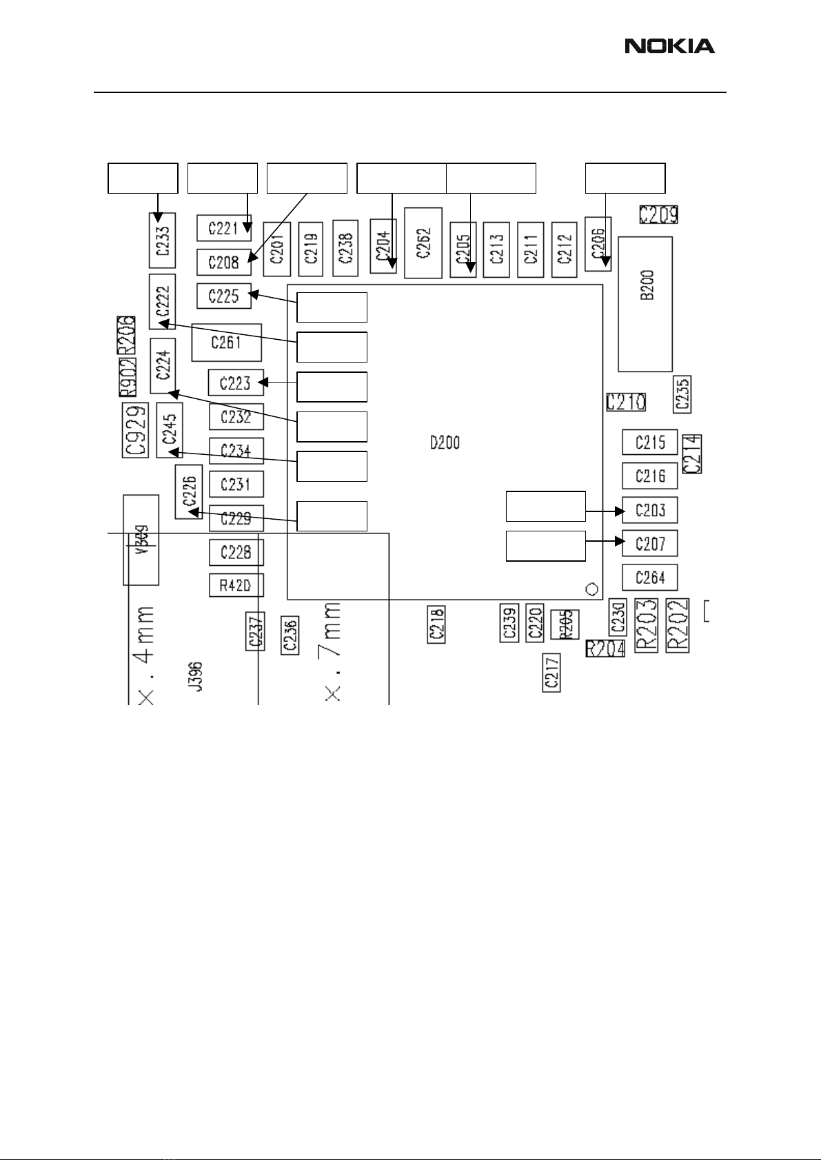
Fig 1 UEM regulator's filter capacitors................................................................................6
Fig 2 BB testpoints ..............................................................................................................7
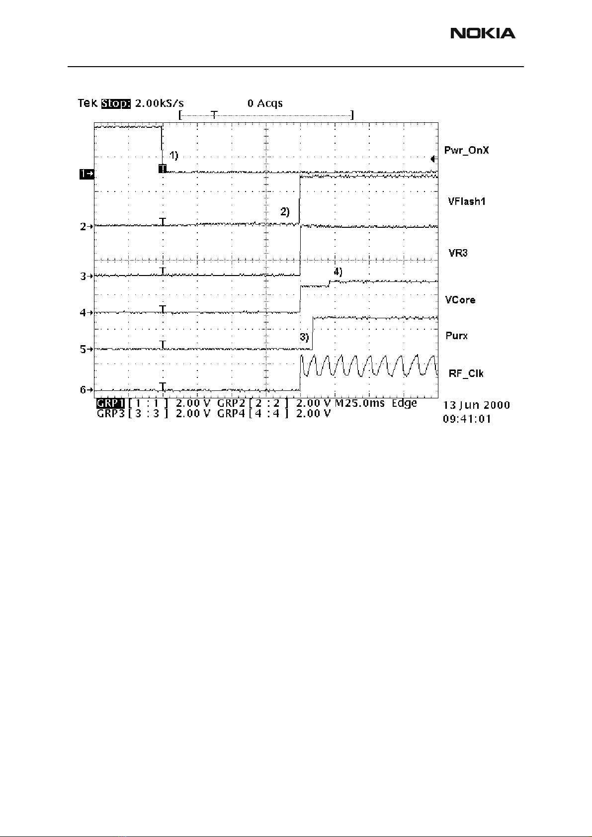
Fig 3 Power up sequence .....................................................................................................10
Fig 4 Fault tree, phone does not power up...........................................................................12
Fig 5 Fault tree, charging ....................................................................................................16
Fig 6 Fault tree, earpiece fail ..............................................................................................18
Fig 7 Fault tree, microphone fail .........................................................................................19
Fig 8 Fault tree, accessory detection....................................................................................20
Fig 9 Fault tree, data cable...................................................................................................21
Fig 10 Fault tree, sleep clock...............................................................................................22
Fig 11 Fault tree, Display/Keyboard lights..........................................................................23
Fig 12 Fault tree, display ....................................................................................................24
Fig 13 Fault tree, infra red ...................................................................................................26

RH-13
Troubleshooting CCS Technical Documentation
Page 4 ãNokia Corporation Issue 1 11/02
Fig 14 Receiver block diagram............................................................................................30
Fig 15 RF Test .....................................................................................................................33
Fig 16 Audio Test ................................................................................................................33
Fig 17 RF Test. ....................................................................................................................34
Fig 18 Fault finding chart. ...................................................................................................36
Fig 19 General checking......................................................................................................37
Fig 20 GSM RSSI Measurement. ........................................................................................38
Fig 21 RX VHF VCO signal level and frequency...............................................................39
Fig 22 UHF VCO.................................................................................................................40
Fig 23 RF controls ...............................................................................................................40
Fig 24 RX I/Q signal............................................................................................................41
Fig 25 IF signal level ...........................................................................................................42
Fig 26 Fault finding chart. ...................................................................................................43
Fig 27 RF Test. ....................................................................................................................44
Fig 28 Fault finding chart ....................................................................................................46
Fig 29 GSM RSSI Measurement. ........................................................................................48
Fig 30 RF controls. ..............................................................................................................49
Fig 31 RX VHF VCO signal level and frequency...............................................................49
Fig 32 UHF VCO signal level and frequency......................................................................50
Fig 33 RF controls. ..............................................................................................................51
Fig 34 RX I/Q signal............................................................................................................51
Fig 35 IF signal level. ..........................................................................................................53
Fig 36 TX signal path. .........................................................................................................54
Fig 37 RF Test. ....................................................................................................................55
Fig 38 RF controls. ..............................................................................................................55
Fig 39 Fault finding chart ....................................................................................................56
Fig 40 TDMA1900. .............................................................................................................58
Fig 41 GSM1900. ................................................................................................................58
Fig 42 Fault finding chart ....................................................................................................59
Fig 43 Power detection. .......................................................................................................61
Fig 44 Fault finding chart for 19.2 MHz oscillator..............................................................64
Fig 45 Fault finding chart for RX VHF VCO......................................................................65
Fig 46 BB PLL.....................................................................................................................66
Fig 47 Fault finding chart for BB PLL. ...............................................................................67
Fig 48 Fault finding chart for TX VHF VCO......................................................................68
Fig 49 Fault finding chart for UHF SYNTHESIZER..........................................................69
Fig 50 Auto tune TDMA .....................................................................................................70
Fig 51 Auto-tune GSM ........................................................................................................72
Fig 52 Fault finding chart ....................................................................................................76

CCS Technical Documentation Troubleshooting
RH-13
Issue 1 11/02 ãNokia Corporation Page 5
Transceiver Troubleshooting
General about testing
Phone operating modes
Phone has three different modes for testing/repairing phone. Modes can be selected with
suitable resistors connected to BSI- and BTEMP- lines as following:
Table 1: Mode selection resistors
The MCU software enters automatically to local or test mode at start-up if correspond-
ing resistors are connected.
Note! Baseband doesn't wake up automatically when the battery voltage is connected
(normal mode). Power can be switched on by
• Pressing the power key
• connecting a charger
• RC-alarm function
In the local and test mode the baseband can be controlled through MBUS or FBUS (FBUS
is recommended) connections by a Phoenix service software.
Mode BSI- resistor BTEMP- resistor Remarks
Normal 68k 47k
Local 560_ (<1k_) What ever
Test 3.3k (> 1k) 560_ (<1k_) Recommended with baseband testing. Same as
local mode, but making a phone call is possible.

RH-13
Troubleshooting CCS Technical Documentation
Page 6 ãNokia Corporation Issue 1 11/02
Measurement points
Figure 1: UEM regulator's filter capacitors
V
R
6
V
R
4
V
R
2
V
R
7
V
R
3
V
R1
B
V
R1
A
V
COR
E
V
FLAS
H
V
FLAS
H
V
AN
A
VSIM
V
I
O
V
R
5
UEM

CCS Technical Documentation Troubleshooting
RH-13
Issue 1 11/02 ãNokia Corporation Page 7
Figure 2: BB testpoints
SLEEPCLK
UEMINT
SLEEPX
PURX
DbusDA
CbusDA
CbusENX
Fbus TX
CbusCLK
DbusCLK
FbusRX
Dbu
sENX
MbusRX
MbusTX
RFCLK:
Init clk
19.22MHz
GSM 13MHz
TDMA
UEM
FLASH
UPP

RH-13
Troubleshooting CCS Technical Documentation
Page 8 ãNokia Corporation Issue 1 11/02
Baseband Troubleshooting
Note: ESN and IMEI has to re-written to phone If UEM is replaced. This can be
done only in Central Service.
The Baseband Troubleshooting instructions consists of the following topics:
•Powerup
• Flash programming
•Audio
•Earpiece
•Microphone
• Charging
• Accessory detection
• Data cable
•Sleepclock
• User interface
•Display
•Lights
•Buzzer
•Vibra
•Keyboard
•Infrared
• Power up faults
Power up sequence
UEM acts as a HW master during start up
• Vbatt limits: 2.1V for internal state machine, 3V triggering whole startup
• Regulator sequencing

CCS Technical Documentation Troubleshooting
RH-13
Issue 1 11/02 ãNokia Corporation Page 9
•Hw "core" regulators "on": Vio, Vcore, VR3, Vflash1
•These regulators are supplying the processors, memory, chip interfaces and
clock source in RF
• Reset releasing delay
•Supply voltages stabilize to their UEM hw default values
•RFCLK grows to full swing
•Core is ready to run but waiting for PURX release
• Reset releasing
•UPP releases the SLEEPX up to "non sleep" -state to prevent the UEM switching
the regulators "OFF"
MCU starts running the Bootstrap Code
•written in stone/ UPP internal ROM
•the program checks if there exists any reason for FDL mode (Flash Down Load)
•If there exists executable code in FLASH and there exists no reason for FDL, the
MCU starts running the MCU program from FLASH.
MCU runs the FLASH MCU code
•the phone initialization, user interfaces, internal blocks etc
•Core regulator voltage setting for required DSP speed
•Initializes the DSP and concerning hw
•Releases DSP reset -> DSP starts running
Note: In the figure below RF_Clk frequency appears to be lower than 19.2MHz
because of too low oscilloscope sampling frequency (2kS/s).

RH-13
Troubleshooting CCS Technical Documentation
Page 10 ãNokia Corporation Issue 1 11/02
Figure 3: Power up sequence
1 Power key pressed
• After 20ms UEM enters RESET MODE if VBAT>Vmstr+
2 2) VFLASH1, Vana, Vcore, Vio and VR3 goes high.
• VCTCXO enabled by VR3 -> RFClk 19.2 MHz running.
3 Purx released
• Purx released by UEM, UEMINT goes high for 100 ms and about
500ms RFCLK will change 13MHz (GSM mode), SleepX goes high and
UEM starts feeding SleepClk (32 KHz) to UPP. NOTE! Sleepclock starts
running in crystal circuitry (B200) immediately when battery voltage is
supplied.
4 Software running
• Default value for Vcore is 1.5 volts and if software is running Vcore will
rise to 1.8 volts.
• Cbus (1.00MHz/GSM and 1.08MHz/TDMA) clock starts running.

CCS Technical Documentation Troubleshooting
RH-13
Issue 1 11/02 ãNokia Corporation Page 11
Phone does not start up normally or does not stay on
Note! In case of power up faults, it's not possible to force phone on by disabling watch-
dog. Instead, measurements should be done immediately when power key pressed or
when battery voltage connected to phone (local/test mode).
The easist way to check if software is running when phone takes abnormal amount of
current is to measure cbusclk and Vcore.
Dbus clock (programmable 9.72MHz TDMA, 13MHz GSM) is not automatically visible on
test and local mode.

RH-13
Troubleshooting CCS Technical Documentation
Page 12 ãNokia Corporation Issue 1 11/02
Figure 4: Fault tree, phone does not power up
Flash Programming does not work
Flash programming procedure
• Phone communicates with prommer via production test pattern, using signals:
Try to start phone to
test or local mode Check the
power key
Check
X101,C108,
C109,Z101
Measure
Vflash1,Vana,Vio,Vcore
,VR3 when pwr key
pressed
Check 13MHz /GSM
or 19.44/TDMA
RF-clock from C420
Check that purx
goes up to 1.8V
Change UPP
(D400)
Change the
UEM (D200)
OK
Measure VBAT
from C262
Check R202,
R203, R205,
C217, C220
Check G801
(missing,
misaligned)
Measure J406.
1.08
MHz/TDMA
and
1.00MHz/GSM
Check
C420
Check 19.2MHz
from G801
See RF
troubleshooting
FAIL
Re-flash phone
OK
OK
FAIL
VR3
missing
FAIL
OK
OK
OK
Check
R816,C867,C8
66, R817, C868
Change
G801
OK
FAIL
FAIL
OK
OK
FAIL
OK
OK
OK
FAIL
Programmng ok,
but phone doesn't
start Go to flash failure
chart
Programming
fails

CCS Technical Documentation Troubleshooting
RH-13
Issue 1 11/02 ãNokia Corporation Page 13
•FBUSTX(serial data to phone),
•FBUSRX(serial data from phone),
•MBUS(serial clock for FBUSRX)
•VPP(External flashing voltage for speed up flashing)
• Also BSI line is used when initializing flashing (battery connector)
• When phone is powered (VBAT>3V ) MBUS and FBUSTX lines are pulled up inter-
nally by phone.
• Prommer sends command to UEM, using FBUSRX, to enter Flash-mode. During
the sending of this command prommer keeps BSI line high and MBUS is used as a
serial clock.
• When Flash-mode command is acknowledged UEM enters Flash-mode and
releases reset (PURX) to MCU.
• After reset is released UPP checks if there is a request for Bootstrap code (that
resides in UPP ROM).
• Request for Bootstrap is MBUS pulled down by Prommer. (If bootstrap is not
requested, bootstrap code jumps to FLASH SW.)
• If Bootstrap code is requested UPP enters Flash-mode and sets FbusTX to '0' as
acknowledgement to prommer. This is an indication that UPP can run, at least,
the fixed Bootstrap code – although not able to run FLASH code. UPP then sends
an UPP-ID to prommer via FBUSTX line.
• After prommer has received UPP-ID it sends corresponding Secondary Boot Code
to phone via FBUSRX. Secondary Boot Code, when run in UPP, requests UPP to
send information to prommer about flash type and other HW related parameters
about the device to be flashed.
• Prommer then sends the Algorithm Code corresponding to the HW parameters
and this algorithm, when run in UPP, takes over handling the MCUSW transfer to
Flash.
• 12 volts can be supplied to Vpp (by prommer) to speedup flashing.
• FLASH Program includes a package of MCU and DSP software and all default
parameters for the phone. The tuning values will be added/rewritten during
Flash/Alignment phase.

RH-13
Troubleshooting CCS Technical Documentation
Page 14 ãNokia Corporation Issue 1 11/02
Flash programming error codes
Error codes can be seen from "FPS-8 Flash" in Phoenix.
Underlined note means that item under consideration is being used first time in flashing
sequence.
Table 2: Flash programming error codes
Error Description Not working properly
C101 "The Phone does not set FbusTx line high after the
startup."
Vbatt
Vflash1
Vcore
VIO
BSI and FbusRX from prommer to UEM.
FbusTx from UPP->UEM->Prommer(SA0)
C102 "The Phone does not set FbusTx line low after the
line has been high. The Prommer generates this
error also when the Phone is not connected to the
Prommer."
PURX(also to Safari)
VR3
Rfclock(VCTCXO->Safari->UPP)
Mbus from Prommer->UEM-
>UPP(MbusRx)(SA1)
FbusTx from UPP->UEM->Prommer(SA1)
C103 "Boot serial line fail." Mbus from Prommer->UEM-
>UPP(MbusRx)(SA0)
FbusRx from Prommer->UEM->UPP
FbusTx from UPP->UEM->Prommer
C104 "MCU ID message sending failed in the Phone." FbusTx from UPP->UEM->Prommer
C105 "The Phone has not received Secondary boot codes
length bytes correctly."
Mbus from Prommer->UEM->UPP(MbusRx)
FbusRx from Prommer->UEM->UPP
FbusTx from UPP->UEM->Prommer
C106 "The Phone has not received Secondary code bytes
correctly."
Mbus from Prommer->UEM->UPP(MbusRx)
FbusRx from Prommer->UEM->UPP
FbusTx from UPP->UEM->Prommer
C107 "The Phone MCU can not start Secondary code cor-
rectly."
UPP
A204 " The flash manufacturer and device IDs in the
existing Algorithm files do not match with the IDs
received from the target phone."
Flash
Signals between UPP-Flash
A387 "The MCU ID in the MCUSW UPP
C601 "The prommer has detected that Vpp voltage level
has dropped below the limit"
Vpp from prommer - >Flash
C383
C583
C683
"The Prommer has not received Phone acknowledge
to the message."
(C383-during algorithm download to target phone)
(C583-during erasing)
(C683-during programming)
Flash
UPP
Signals between UPP-Flash

CCS Technical Documentation Troubleshooting
RH-13
Issue 1 11/02 ãNokia Corporation Page 15
C384
C584
C684
"The Phone has generated NAK signal during data
block transfer."
(C384-during algorithm download to target phone)
(C584-during erasing)
(C684-during programming)
Flash
UPP
Signals between UPP-Flash
C585
C685
Data block handling timeout"
(C585-during erasing)
(C685-during programming)
Flash
UPP
Signals between UPP-Flash
C586
C686
"The status response from the Phone informs about
fail."
(C586-during erasing)
(C686-during programming)
Flash

RH-13
Troubleshooting CCS Technical Documentation
Page 16 ãNokia Corporation Issue 1 11/02
Charging
Note: Charging voltage and current can be checked by connecting phone to service
software and reading ad- converter values of vchar and ichar.
Figure 5: Fault tree, charging
Audio failures
In case of audio failures there are three possibilities to check audio lines.
1 Make a phone call against tester and check audios.
2 In case of earpiece/XMIC fail: Feed 1Khz signal to XMIC line and measure signal
from earpiece line. Audio test box JBA-8 is needed. Audio loop (Audio test/Ext In
Hp Out) must be switched on by Phoenix service software. This loop will connect
audios only through UEM. In this case UPP is not used.
Phone doesn't start
charging
Connect charger and
check VCHARIN,
check CHRG_CTRL
if used ACP-9,
LCH-8, LCH-9,
DCH-12, HFU-2
Change the
UEM
Check
F100,L100,V100,C105
,R107,C107
Check bottom
connector
-VIN
- CHRG_CTRL
Check
R202,R203,R205,C217,
C220,C201,C202 and
R200
Fail
OK
Check ICHAR
OK
FAIL
OK

CCS Technical Documentation Troubleshooting
RH-13
Issue 1 11/02 ãNokia Corporation Page 17
3 In case of internal microphone/XEAR fail: Feed tone to microphone and measure
signal from XEAR line. Audio test box JBA-8 is needed. Audio loop (Audio test/Hp
In Ext Out) must be switched on by Phoenix service software. This loop will con-
nect audios only through UEM. In this case UPP is not used.
4 Run audio- loop selftest with Phoenix (BB Self tests/ST_EAR_DATA_LOOP_TEST).
This loop will test the eardata/micdata lines between UPP and UEM.

RH-13
Troubleshooting CCS Technical Documentation
Page 18 ãNokia Corporation Issue 1 11/02
Earpiece or external microphone line does not work
Figure 6: Fault tree, earpiece fail
Earpiece doesn't
work
Run audio-loop
selftest with
phoenix
Check R157,L152,
L158,C150,C164,
C153, C165,R152,
C156,C155,R164,
R161,R153,R150,
C159,C167,V153
Check
earpiece
Change UEM
Feed 1KHz to Xmic
by JBA-8 and
measure from
earpiece
Change UPP
Fail
OK
OK
OK
Fail
OK

CCS Technical Documentation Troubleshooting
RH-13
Issue 1 11/02 ãNokia Corporation Page 19
Microphone or XEAR does not work
Figure 7: Fault tree, microphone fail
Microphone doesn't
work
Run audio-loop
selftest with
phoenix
Check
C151,C152,C157,L151,C162,
C168,C169,R156,R162,R166,
R159,C154,C158,C161,C166,
R163,L159,V152
Check
microphone
Change UEM
Feed 1KHz to Mic
and measure from
Xear by JBA-8
Change UPP
Fail
Ok
Ok
Ok
Ok
Fail

RH-13
Troubleshooting CCS Technical Documentation
Page 20 ãNokia Corporation Issue 1 11/02
Accessory detection
• - Start phone to normal mode when checking accessory detection.
• - Ad- converter value of headint and hookint - lines can be checked with Phoenix
ADC-reading.
• - When headset HDC-9 connected and headset push button is held down, head-
int- value should be between 10 and 50 and hookint- value between 0-30.
Figure 8: Fault tree, accessory detection
Accessory detection
doesn't work normally
Check HeadInt and
HookInt ad-value with
Phoenix
(No accessory
connected)
- HeadInt and HooInt
~1000
Change UEM
Check headint-line
L152,C150,R152,C153,
R154,
C160,R153,R150,C159
Check hookint-line
L159,R163,C158,R155,
R151,C161,V152
Check bottom
connector
Connect HDC-9 and keep the
HDC-9 switch close while
reading headint and hookint
ad-value.
Both values should go close to
zero (~0...50)
Ok
Fail Fail
Ok
Ok
Ok
O
k
Calibrate ADC
and check
accessory
detection again
Table of contents
Other Nokia Cell Phone manuals

Nokia
Nokia TA-1449 User manual

Nokia
Nokia Lumia 625 User manual

Nokia
Nokia Asha 311 User manual

Nokia
Nokia TA-1417 User manual

Nokia
Nokia 207 User manual

Nokia
Nokia N Series User manual

Nokia
Nokia 5230 User manual

Nokia
Nokia COMMUNICATOR 9200 Instruction Manual

Nokia
Nokia Lumia 1320 User manual

Nokia
Nokia 1508I User manual

Nokia
Nokia 6255 User manual

Nokia
Nokia N97-5 User manual

Nokia
Nokia 101 User manual

Nokia
Nokia X Specification sheet

Nokia
Nokia 3570 - Cell Phone - CDMA User manual

Nokia
Nokia CLASSIC 6220 User manual

Nokia
Nokia 8208 User manual

Nokia
Nokia Lumia 920 User manual

Nokia
Nokia 6020 - Cell Phone 3.5 MB User manual

Nokia
Nokia RAE-6 Guide