NORMARC 7033 User manual

©1999 Navia Aviation AS
NORMARC 7033
INSTRUMENT LANDING SYSTEM
TRANSMITTER DESCRIPTION

©1999 Navia Aviation AS

©1999 Navia Aviation AS Table of contents
TRANSMITTER DESCRIPTIONNORMARC 7033
INSTRUMENT LANDING SYSTEM
iii
TABLE OF CONTENTS
1 FUNCTIONAL DESCRIPTION ........................................................................9
2 DETAILED DESCRIPTION..............................................................................11
2.1 Transmitter block diagrams................................................................................11
2.2 LF1223A Low Frequency Generator..................................................................14
2.2.1 NMP110A Low Frequency Generator Control.............................................14
2.3 OS1221B RF Oscillator......................................................................................15
2.4 GPA1231A Glidepath Course Power Amplifier Assembly..................................17
2.4.1 GPA1232A Glidepath Clearance Power Amplifier Assembly......................19
2.4.2 PA1234A Power Amplifier ...........................................................................20
2.4.3 AC1226A Amplitude control.........................................................................21
2.4.4 PC1225B Phase Control..............................................................................21
2.4.5 FD1236A Feedback Detector......................................................................21
2.4.6 CD1238A Combiner Detector......................................................................23
2.5 COA1207C Change-Over Assembly..................................................................23
3 TESTS AND ADJUSTMENTS.........................................................................25
3.1 Transmitter Alignments and Calibration.............................................................25
3.1.1 RF Phase Feedback Adjustment.................................................................25
3.1.2 RF Power.....................................................................................................25
3.1.3 LF Phase Adjustment ..................................................................................26
3.1.4 RF Power Balance Adjustment....................................................................27
3.1.5 RF Phase at Combiner I/P...........................................................................28
3.1.6 SDM Calibration...........................................................................................29
3.1.7 DDM Calibration ..........................................................................................29
3.1.8 Ident Tone Modulation Depth ......................................................................29
3.1.9 RF Frequency Adjustment...........................................................................30
3.2 Antenna System Adjustments............................................................................30
3.3 Adjustment points...............................................................................................31
3.4 Frequency configuration strap settings ..............................................................33


©1999 Navia Aviation AS List of Figures
TRANSMITTER DESCRIPTIONNORMARC 7033
INSTRUMENT LANDING SYSTEM
v
LIST OF FIGURES
Figure 1-1 System Block Diagram of a 2-Frequency GP Transmitter ....................10
Figure 2-1 NM 7033 Transmitter Block Diagram part 1 .........................................12
Figure 2-2 NM 7033 Transmitter Block Diagram part 2 .........................................13
Figure 2-3 NMP110A block diagram. .....................................................................15
Figure 2-4 OS1221B block diagram. .....................................................................16
Figure 2-5 Physical organization of power amplifier assembly. .............................18
Figure 2-6 Changeover system block diagram. .....................................................24
Figure 3-1 LF phase CSB illustration. ....................................................................26
Figure 3-2 LF phase SBO illustration. ....................................................................26
Figure 3-3 Power balance SBO illustration. ...........................................................28
Figure 3-4 RF phase SBO illustration ....................................................................28
Figure 3-5 Front side adjustment points. ...............................................................31
Figure 3-6 Power Amplifier Assembly adjustment points (rear view). ....................32


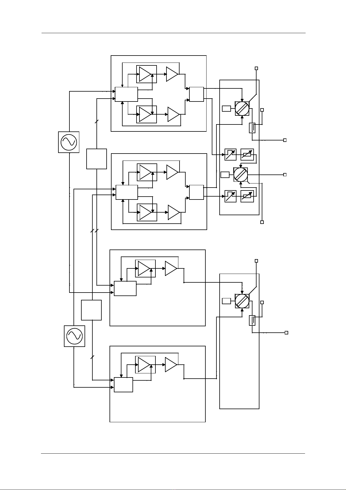
FUNCTIONAL DESCRIPTION
NORMARC 7033
1-9
INSTRUMENT LANDING SYSTEM
TRANSMITTER DESCRIPTION
©1999 Navia Aviation AS
DESCRIPTION OF NORMARC 2-FREQUENCY TRANSMITTER
1 Functional Description
The transmitter section generates the ILS signal with the required RF power levels and modu-
lations levels. The section comprises two identical transmitters, TX 1 and TX 2, where one is
connected to the antenna, while the other is connected to dummy loads, acting as a back-up.
The reference signals in the transmitter section are RF signals from the oscillator OS1221AB
and LF modulation signals (90Hz and 150Hz) from the low frequency generator LF1223A.
System DC voltages comes from the Power Supply board PS1227A.
In each transmitter, the RF oscillator has separate outputs for Course and Clearance. These
two channels are offset by 10 kHz. The LF Generator also has independent outputs for
Course and Clearance. Clearence transmitter is however not included in this single frequency
equipment.
The GPA 1231A Glidepath Course Power Amplifier Assembly contains modules to modulate,
amplify and combine signals into the required CSB and SBO signals. Amplitude- and RF
phase feedback ensures correct RF power level and modulation.
The Clearance transmitters GPA1232A generate only CSB signals, and only amplitude feed-
back is therefore incorporated.
The COA 1207A/C Change Over section has relays to connect the CSB and SBO outputs
from one transmitter to the antenna while the other is connected to dummy loads. The relays
are controlled by a Coax-control signal. SBO phase shifters and attenuators are incorporated
for obtaining the correct CSB/SBO relationship.
The block diagram is shown on the next page.
NORMARC 7033
INSTRUMENT LANDING SYSTEM
TRANSMITTER DESCRIP-
FUNCTIONAL DESCRIPTION ©1999 Navia Aviation AS
1-10
Figure 1-1 System Block Diagram of a 2-Frequency GP Transmitter
PHASER ATTENUATOR
PHASER ATTENUATOR
COAX
RELAY
COAX
RELAY
CSB
CSB
SBO
SBO
OUTPUT
SBO COURSE
OUTPUT
CSB COURSE
MONITOR
CSB
COUPLER
COAX CONTROL
COAX CONTROL
COAX
RELAY
OUTPUT
CSB CLEARANC
E
MONITOR
CSB
COUPLER
COAX CONTROL
RF OSC.
TX2
RF OSC.
TX1
LF GEN.
TX1
LF GEN.
TX2
CHANGE
OVER COU
CHANGE
OVER CLR
CSB
CSB
POWER AMPLIFIER ASSEMBLY COU-TX2
POWER AMPLIFIER ASSEMBLY COU-TX1
POWER AMPLIFIER ASSEMBLY CLR-TX1
POWER AMPLIFIER ASSEMBLY CLR-TX2
AMPLITUDE FEEDBACK
AM-MOD. HPA
FEEDBACK
CONTROL
AMPLITUDE FEEDBACK
AM-MOD. HPA
FEEDBACK
CONTROL
AMPLITUDE & RF PHASE FEEDBACK
AM-MOD. HPA
HPA
HYBRID
FEEDBACK
CONTROL
AM-MOD.
AMPLITUDE & RF PHASE FEEDBACK
50 ohm
50 ohm
50 ohm
AMPLITUDE & RF PHASE FEEDBACK
AM-MOD. HPA
HPA
HYBRID
FEEDBACK
CONTROL
AM-MOD.
AMPLITUDE & RF PHASE FEEDBACK
HBK 591-1

NORMARC 7033
INSTRUMENT LANDING SYSTEM
TRANSMITTER DESCRIP-
DETAILED DESCRIPTION ©1999 Navia Aviation AS
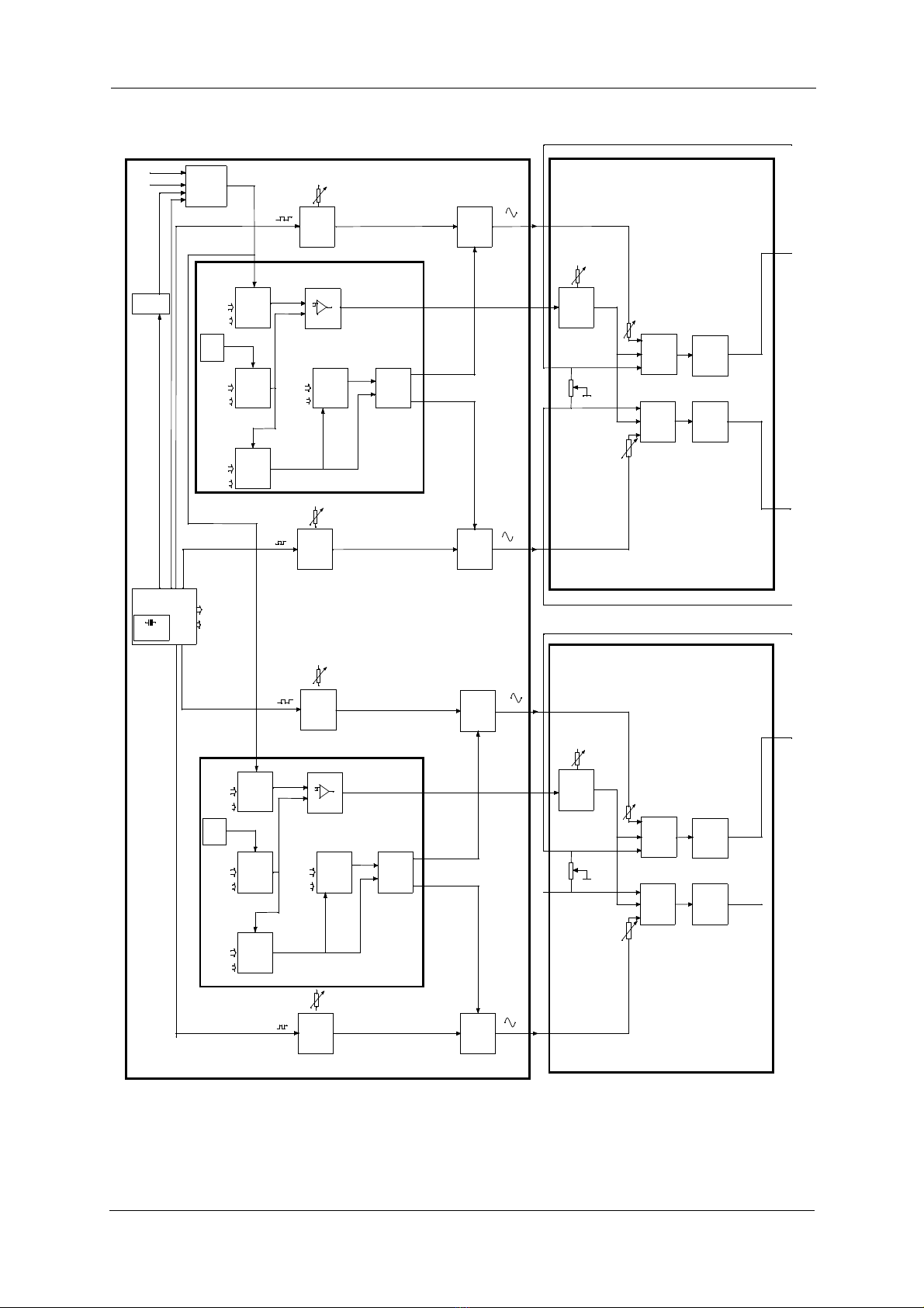
2-12
Figure 2-1 NM 7033 Transmitter Block Diagram part 1
VOLT-
AGE
REF.
DATA (7:0)
DATA (7:0)
DATA (7:0)
CONTROL
CONTROL
CONTROL
MOD
LEVEL
RF
LEVEL DDM
DAC
DIFFER-
ENTIAL
DISTRI-
BUTION
IDENT
KEYER
IDENT + DC LEVEL
MOD 90 LEVEL
MOD 150 LEVEL (DC)
LF_DIG
DATA (7:0)
CONTROL
IDENT/
VOICE
SELECTOR
VOICE
VOICE ON/OFF ANALOGUE IDENT/VOICE
90 Hz
LOWPASS
FILTER
AGC
AMPLIFIER
150 Hz
LOWPASS
FILTER AGC
AMPLIFIER 150 Hz COU
ANLG_ID
LPF_1020
LP FILTER
MOD_AMP
AGC_AMP2
AGC_AMP
LPF_150
LPF_90
DIGITAL AUDIO
GENERATOR &
CONTROLS
3.6864MHz
Vref
Vref
Vref
Vref
VOLT-
AGE
REF.
DATA (7:0)
DATA (7:0)
DATA (7:0)
CONTROL
CONTROL
CONTROL
MOD
LEVEL
RF
LEVEL DDM
DAC
DIFFER-
ENTIAL
DISTRI-
BUTION
IDENT
KEYER IDENT + DC LEVEL
MOD 90 LEVEL
MOD 150 LEVEL
DATA (7:0)
CONTROL
90 Hz
LOWPASS
FILTER
AGC
AMPLIFIER
150 Hz
LOWPASS
FILTER
AGC
AMPLIFIER
90 Hz CLR
150 Hz CLR
MOD_AMP2
AGC_AMP4
AGC_AMP3
LPF_1502
LPF_902
Vref
Vref
Vref
Vref
LF1223A
90 HZ COU
COU
CLR
DAC
DAC
DAC
UNREG 150 Hz
UNREG 90 Hz
UNREG 90 Hz
UNREG 150 Hz
RF BAL
BUFFER
AC1226A
COMPA-
RATOR
AMP_90
MODU-
LATION
CURRENT
DRIVER
AMP_90
MODU-
LATION
CURRENT
DRIVER
AMP_150
COMPA-
RATOR
AMP_150
MOD DEPTH
90 Hz
MOD DEPTH
150Hz
DC
(RF power)
90 Hz FEEDBACK
150 HzFEEDBACK
AC1226A
150 Hz CLR
PHASE ADJ.
90 Hz CLR
PHASE ADJ.
150 Hz COU
PHASE ADJ.
90 Hz COU
PHASE ADJ.
DATA (7:0)
CONTROL
RF BAL
BUFFER
AC1226A
COMPA-
RATOR
AMP_90
MODUL-
ATION
CURRENT
DRIVER
AMP_90
MODUL-
ATION
CURRENT
DRIVER
AMP_150
COMPA-
RATOR
AMP_150
MOD DEPTH
90 Hz
MOD DEPTH
150Hz
DC
(RF power)
90 Hz FEEDBACK
150 HzFEEDBACK
AC1226B
MOD 90 Hz
MOD 150 Hz
150 Hz FEEDBACK
90 Hz FEEDBACK
MOD 90 Hz
MOD 150 Hz
90 Hz FEEDBACK
1
2
3
4
5
6
(RF POWER)
(RF POWER)
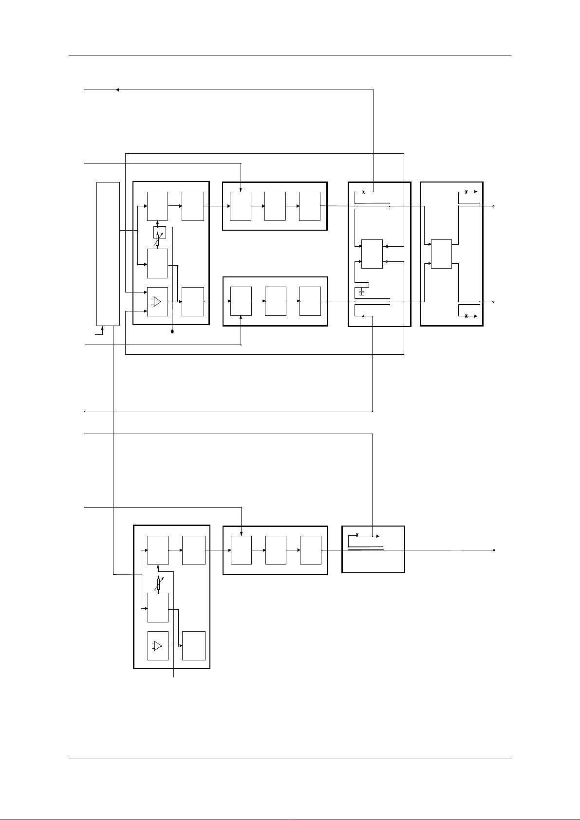
DETAILED DESCRIPTION
NORMARC 7033
2-13
INSTRUMENT LANDING SYSTEM
TRANSMITTER DESCRIPTION
©1999 Navia Aviation AS
Figure 2-2 NM 7033 Transmitter Block Diagram part 2
PC1225B
RF
PHASE
REGU-
LATOR
RF
PHASE
REGU-
LATOR
AMPLIFIER
AMPLIFIER
MODU-
LATOR DRIVER LOWPASS
FILTER
PA1234A
MODU-
LATOR DRIVER LOWPASS
FILTER
PA1234A
90°
HYBRID
RF PHASE ADJ
FD1236A
90°
HYBRID
CSB COU
SBO COU
CD1238A
OS1221B
SYNTHE-
SIZER
Tx ON/OFF
RF PHASE FEEDBACK
RF PHASE FEEDBACK
MODU-
LATOR DRIVER LOWPASS
FILTER
PA1234A
CSB CLR
PHASE
FEEDB.
OFFSET
ADJ.
PHASE OUT
PC1225B
RF
PHASE
REGULATOR
RF
PHASE
REGULATOR
AMPLIFIER
AMPLIFIER
PHASE OUT
PHASE
FEEDB.
OFFSET
ADJ.
FD1224A
1
2
3
4
5
6
HBK 750B-1

NORMARC 7033
INSTRUMENT LANDING SYSTEM
TRANSMITTER DESCRIP-
DETAILED DESCRIPTION ©1999 Navia Aviation AS
2-14
2.2 LF1223A Low Frequency Generator
General Description:
LF1223A provides the audio signals to be modulated onto the carrier signal in the transmitter
(AC 1226A). The levels of the 90Hz, 150Hz, RF level and ident signals and the morse code of
the ident signal are programmable from the RMS.
Block Diagram:
See Figure 2-1.
Block Description:
DIGITAL SECTION
The LF_DIG block provides the interface to the RMS, the parameter storage (EEPROM) and
the analog section. All sequencing and local parameter update is performed by this block.
Most of the functionality of the DIGITAL SECTION is handled by the NMP110A FPGA
described in chapter 2.2.1.
ANALOG SECTION.
All levels are controlled digitally through multiplying DACs (MDACs), and the AC levels are
stabilized through AGC amplifiers. The fine tuning of the phase between the 90 and 150Hz
signals is done manually with potentiometers. The morse code is keyed in an analog multi-
plexer, and can be synchronized with a DME.
RF level and ident (DC_IDENT), SDM and DDM (90/150Hz) are generated in the MDAC
chain. Multiplication (m) in the MDACs are 0≤m<1.
• The reference voltage is multiplied in the first MDAC to form the DC portion of DC_IDENT.
The keyed 1020Hz sine wave is multiplied in an other MDAC to control the ident amplitude,
this signal forms the IDENT portion of DC_IDENT signal.
• The DC portion of DC_IDENT is multiplied in the third MDAC to form the modulation sum
reference .
• This modulation sum reference is split in two signals where one is modified by a fourth
MDAC before they are combined again to form the modulation difference.
2.2.1 NMP110A Low Frequency Generator Control
General description:
NMP110A is a FPGA within the LF_DIG block. It provides the interface between the RMS and
the local parameter storage and sequencing of the LF signals are performed here. NMP110A
is based on the Actel ACT1020 FPGA. For electrical specifications see the ACT1020
datasheet.

DETAILED DESCRIPTION
NORMARC 7033
2-15
INSTRUMENT LANDING SYSTEM
TRANSMITTER DESCRIPTION
©1999 Navia Aviation AS
Block diagram:
Figure 2-3 NMP110A block diagram.
Block description:
FREQUENCY DIVIDER
divides the system clock (3.6864MHz) into 30Hz, 90Hz, 150Hz, 1020Hz, morse code tick
length and morse code word length clock signals.
IDENT SEQUENCER
generates the programmed ident envelope for the ILS signal and external DME equipment.
CONTROL SECTION
includes the RMS interface, address decoding, configuration control and automatic refresh of
the DACs and the other registers. The refresh cycle is performed after a completed RMS
access cycle.
2.3 OS1221BRF Oscillator
General Description:
The OS1221B module generates the RF signals used for the generation of the carrier signals
in the transmitters (ch. 2.5).
Configuration
Storage
Counter
Ident Sequencer
Refresh Address
Sequencer
RMS interface
DME_IDNT_IN, DME_ACTIVE
Address
Decoder
MUX
EXT_SERVICE
*_CS,DAC_A
IOCSB
CLK
TST30
CLR90
CLR150
COU90
COU150
IDNT_DIG
DME_IDNT_OUT
IDNT_ON
IOS*
IOD*
Control
Control Section
F
requency
Di
v
id
er
ADDR*
COAX_POS, LF_ADDR
HBK563-1

NORMARC 7033
INSTRUMENT LANDING SYSTEM
TRANSMITTER DESCRIP-
DETAILED DESCRIPTION ©1999 Navia Aviation AS
2-16
Block Diagram:
Figure 2-4 OS1221B block diagram.
Block Description:
The RF signal is generated by a voltage controlled oscillator (VCO) built around a Dual Gate
Mosfet Transistor, chosen because of its good noise properties, and the possibility to have an
isolated output at the drain.
A part of the signal is fed back, via a buffer for isolation, to a divide by 64, modulus 2 pres-
caler. This is connected to a MC145152-2, a phase locked loop circuit that performs the
counting and control of the prescaler. The total count, and thereby the frequency, is set by
inserting shunts onto an array of pins.
The correct count for a desired frequency (FRQ) is found as follows:
CHANNEL
SELECT COU
PROGRAMABLE
DIVIDER
RF
OSCILLATOR
PHASE
DETECTOR LOWPASS
FILTER VCO
LOCK
DETECT
WINDOW
COMP.
BANDPASS
FILTER
12 dB OSC_
C
64
MODULUS 2
DIVIDER
COU Tx ON/OFF
X-TAL
FREQ.
TEST
POINT
FREQUENCY
ADJUST
MODULUS SELECT
LOCK DETECT TO IIC BU
S
SCHM.TR
LATCH
SCHM.TR
LOCK DETECT TO IIC BU
S
LOCK DETECT TO IIC BU
S
CHANNEL
SELECT COU
PROGRAMABLE
DIVIDER
RF
OSCILLATOR
PHASE
DETECTOR LOWPASS
FILTER VCO
LOCK
DETECT
WINDOW
COMP.
BANDPASS
FILTER
12 dB OSC_
C
64
MODULUS 2
DIVIDER
MODULUS SELECT
LOCK DETECT TO IIC BU
S
SCHM.TR
LATCH
SCHM.TR
LOCK DETECT TO IIC BU
S
LOCK DETECT TO IIC BU
S
CLR Tx ON/OFF HBK587-3

DETAILED DESCRIPTION
NORMARC 7033
2-17
INSTRUMENT LANDING SYSTEM
TRANSMITTER DESCRIPTION
©1999 Navia Aviation AS
COUNT = FRQ / 7.5011KHZ
In order to set the frequency on the OS1221, the count must be rounded off to the nearest
integer value and converted to a binary number.
Insert shunts for binary zeros on the pin arrays P2 or P102 (COU/CLR) starting with the most
significant bit on P2/102,A0 and the least significant bit on P2/102,N9. Be aware that most cal-
culators discards leading zeros. Please find tables of jumper settings in chapter 3.4.
The internal oscillator of the Course PLL is also used to control the Clearance PLL.
The differential output of the phase comparator is made single ended by a balanced amplifier.
A combined low-pass filter and integrator is built around an operational amplifier, that gener-
ates the control voltage for the RF oscillator. This control voltage is also fed to a window com-
parator that alarms the system via the I2C-bus if it falls outside its limits (another control of the
PLL is via the Lock Detect output of the PLL). The Lock Detect output of the PLL circuit is fed
to a low pass filter and a transistor. This output consists of narrow negative going pulses when
the loop is locked, and wide pulses of variable width when out of lock. Therefore the transistor
will be turned off when in lock, and on when out of lock.
The output from the transistor goes to two Schmidt triggers, one latching and one unlatching.
The latching Schmidt triggers turns the signal off if the loop goes out of lock and alarms the
I2C-bus. It is reset by power on and/or a low transition of the COU_OFF signal (CLR_OFF for
the clearance channel). The other Schmidt trigger is used to inform the system of the situation
that the loop have been out of lock, but is in lock at the present time even if the signal is turned
off (this might be the situation if a short drop in the 12V supply occurs, or a change in fre-
quency setting has taken place).
The signal switching is done in two steps. The first is a diode switch and the next is a Dual
Gate Mosfet transistor that can be turned off by taking its control gate to a low potential. This
transistor acts as a buffer for the signal when in the on state. At the output of this transistor, a
second order bandpass filter follows, that serves as an output match of the transistor and to
filter out harmonics of the output voltage. The last stage is a 12dB gain block that delivers
10mW of power to the PC1225 card.
The Clearance channel is identical to the Course channel except for the crystal oscillator for
the PLL.
2.4 GPA1231A Glidepath Course Power Amplifier Assembly

NORMARC 7033
INSTRUMENT LANDING SYSTEM
TRANSMITTER DESCRIP-
DETAILED DESCRIPTION ©1999 Navia Aviation AS
2-18
Physical Organization
Figure 2-5 Physical organization of power amplifier assembly.
FD 1xxxx
PA 123xx *)
PC 1xxxx
CD 123xx *)
AC 1226x
C1 C2 C3 C4
J16
J15
J1
J2
J3
J10J11J12J13
J7
J6
J8
J14
J9
TP1 J17
HBK695-2
PA 123xx
*) Not present in GP-CLR

DETAILED DESCRIPTION
NORMARC 7033
2-19
INSTRUMENT LANDING SYSTEM
TRANSMITTER DESCRIPTION
©1999 Navia Aviation AS
General Description:
The Glidepath Course Power Amplifier Assembly GPA1231A consists of the following mod-
ules mounted together as shown on Fig. 2-5.
The GPA1231A receives RF signals and LF signals from the OS1221B Oscillator (Ch. 2.3)
and LF1223A low frequency generator (Ch. 2.2) respectively. The outputs from the
GPA1231A are carrier sideband (CSB) signal and sideband only (SBO) signal. Detected sam-
ples of the CSB and SBO signals and the phase feedback signal are available on the BNC
connectors on the front panel. Information about signals and status are interfaced with the
RMS.
Block Diagram:
See Figure 2-1 and Figure 2-2.
Block Description:
The PC1225B Phase Control receives the RF signal from the oscillator OS1221B and splits
this signal into two paths (90Hz and 150Hz branch). The RF phase regulator blocks ensure
correct phase relationship between the 90Hz and 150Hz modulated RF signals prior to com-
bining them into CBS and SBO signals.
The AC1226A Amplitude Control provides and controls the required LF modulation signals
(90Hz and 150Hz) for the PA 1234A power amplifiers that keeps the output RF level and
amplitude modulation constant.
The PA1234A Power Amplifier modulates the incoming RF signal from PC1225B with a 90Hz
or a 150Hz LF signal to obtain an AM-signal and amplifies the modulated signals.
The FD1236A Feedback Detector provides feedback signals for amplitude and phase correc-
tion of the 90 and 150 Hz modulated RF signals.
The CD1238A Combiner Detector combines the 90 Hz modulated RF signal and the 150 Hz
modulated RF signal in such a way that true CSB and SBO RF signals are generated. In addi-
tion, detected and filtered CSB and SBO signals for measurement purposes are provided to
the test connectors on the front panel.
Detailed description about the individual modules are found below.
2.4.1 GPA1232A Glidepath Clearance Power Amplifier Assembly
General description:
The Glidepath Course Power Amplifier Assembly GPA1231A consists of the following mod-
2 Power Amplifiers PA1234A
1 Amplitude Control AC1226A
1 Phase Control PC1225B
1 Feedback Detector FD1236A
1 Combiner Detector CD1238A

NORMARC 7033
INSTRUMENT LANDING SYSTEM
TRANSMITTER DESCRIP-
DETAILED DESCRIPTION ©1999 Navia Aviation AS
2-20
ules
The GPA1232A contains the RF blocks in the GP Clearance transmitter system. It receives
RF signals and LF signals from the OS1221B oscillator and LF1223A low frequency generator
respectively. The output of the GPA1232A is a carrier sideband (CSB) signal. Detected sam-
ple of the CSB signal is available on the front panel. Other system parameters are transmitted
to the RMA1215A.
Block Diagram:
See transmitter block diagram.
Block Description:
The PC1225B Phase Control receives the RF signal from the oscillator OS1221B. The RF sig-
nal is fed into the 90Hz branch and further through buffers and amplifiers. The 150Hz branch
is inactive.
The PA1234A Power Amplifier modulates the incoming RF signal from PC1225B with a CBS
LF signal to obtain an AM-signal and amplifies it.
The AC1226B Amplitude Control generates the required CSB LF modulation signal to the
power amplifier, to keep the output RF level and amplitude modulation constant.
The FD1224A Feedback Detector provides a feedback signal for amplitude correction of the
CSB modulated RF signal.
2.4.2 PA1234A Power Amplifier
General Description :
Power amplifier PA1234A is a three stage single-ended amplifier.
The first stage works as an AM-modulator. The modulation tone (90Hz or 150Hz) is fed to the
collector of a bipolar transistor. This modulation stage is operating in class C and has imped-
ance matching network at both input and output. Nominal RF input level is approximate
20dBm.
Second stage consists of a 5W MOSFET-transistor operating in class B. The input impedance
network is matched to 50Ω, while the output impedance network is matched to the complex
conjugated impedance of the third stage transistor. This stage has a collector-to-gate feed-
back and a input shunt loading resistor at the transistor gate, to prevent unwanted oscillations
and keep the transistor unconditionally stable.
Third stage is a 30W MOSFET-transistor operating in class AB. Its output impedance network
consists of microstrip transmission lines and a variable capacitor to achieve maximum power
and efficiency. This stage has also feedback and shunt resistors to prevent unwanted oscilla-
tions. As gain control, both the second and third stage have potentiometers to set the operat-
ing point. A positive voltage regulator is used to keep a fixed input voltage to these gain
control circuits.
1 Power Amplifier PA1234A
1 Amplitude Control AC1226B
1 Phase Control PC1225B
1 Feedback Detector FD1224
Table of contents
Popular Transmitter manuals by other brands

iKarus
iKarus Opticc 6 Sport instruction manual

RKI Instruments
RKI Instruments 65-2322-04SS Operator's manual

ATIM
ATIM Cloud Wireless DINRS user guide

NEUTRIK
NEUTRIK xirium pro user manual

Mod-tronic
Mod-tronic Cecomp F16DR manual

Greyline Instruments
Greyline Instruments Tank Farm Transmitter TFT32 user guide


Applied Wireless
Applied Wireless AT900-32 user guide

Kindermann
Kindermann Multishare 31 operating instructions

dymax
dymax BlueWave MX-275 user guide

Primex
Primex XR TIME SYNCHRONIZATION Installation & user guide

Monacor
Monacor IMG Stage Line TXS-820LT quick guide

Pavone Systems
Pavone Systems DAT 1400 Technical manual