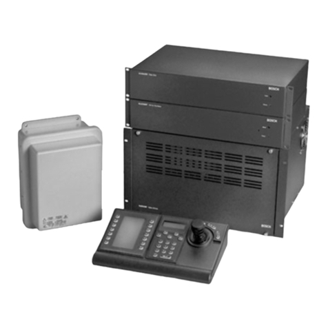
Northern Telecom BCS35 Parts list manual

BCS35 and up Standard 01.03 August 1996
297-1001-536
Distributed Processing Peripheral
Card Replacement Guide
DPP
DPP


DPP Card Replacement Guide BCS35 and up
DMS-100 Family
Distributed Processing Peripheral
Card Replacement Guide
YearPrev1996 Northern Telecom
All rights reserved.
Printed in Canada and printed in the United States of America.
Information is subject to change without notice. Northern Telecom reserves the right to make changes in design or components
as progress in engineering and manufacturing may warrant.
DMS
,
DMS SuperNode
,
MAP, and
NT are trademarks of Northern Telecom.
Publication number: 297-1001-536
Product release: BCS35 and up
Document release: Standard 01.03
Date: August 1996

297-1001-536 Standard 01.03 August 1996
ii
Publication history
August 1996 Standard release 01.03 for software release BCS36 and up. This version
includes changes to this "Publication history" page.
December 1993
Standard release 01.02 for software release BCS36 and up.

DPP Card Replacement Guide BCS35 and up
iii
Contents
Circuit pack replacement 1–1
How to use this document 1–1
General information about circuit pack failures 1–1
Troubleshooting – no specific fault indicators 1–2
Changing processor modes 1–4
Central Processor Unit (CPU) 2–1
General description 2–1
Central processor unit LED display 2–2
Replacing CPU circuit pack 2–2
EPROM circuit pack 3–1
General description 3–1
Replacing EPROM integrated circuits 3–1
EPROM IC precautions 3–2
Memory expansion circuit pack 4–1
General description 4–1
Replacing the Memory Expansion circuit pack 4–1
Error Control II and Error Control II Jumper circuit packs 5–1
General description 5–1
Error control II circuit pack LED 5–1
Error control II circuit pack jumper LED 5–2
Replacement procedures 5–2
QSIO circuit pack 6–1
General description 6–1
Replacing QSIO circuit pack 6–2
56K Interface circuit pack 7–1
General description 7–1
Replacing the 56K Interface circuit pack 7–2
DISK Interface circuit pack 8–1
General description 8–1
Replacing the Disk Interface circuit pack 8–1

iv Contents
297-1001-536 Standard 01.03 August 1996
SCSI Interface circuit pack – turbo only 9–1
General description 9–1
Replacing the SCSI circuit pack 9–2
Data Stream Interface circuit pack 10–1
General description 10–1
DSI primary function 10–1
DSI cable adapter assemblies 10–1
Bus terminator circuit pack 11–1
General description 11–1
Replacing Bus terminator circuit pack 11–1
Power and alarm communications
circuit pack 12–1
Replacing P/A COMM circuit pack 12–2
Disk Crossover and Controller
circuit packs 13–1
General description 13–1
Replacing Disk Controller circuit pack 13–1
Disk controller circuit pack 13–7
SCSI Crossover circuit pack 14–1
General Description 14–1
Replacing the SCSI circuit pack 14–1
56K Crossover circuit pack 15–1
General Description 15–1
Replacing 56K Xovr circuit pack 15–1
Four–channel communication
circuit pack 16–1
General description 16–1
Connector panel 16–1
Four–Channel Comm circuit pack 16–1
Replacing the Four–channel comm pack 16–2
Power supplies 17–1
Powering down DPP for maintenance 17–1
DPP system fuses 17–2
Replacing power supply for maintenance 17–3
List of Figures
Figure 3–1 CPU with DMA (A1 and B1) circuit pack (NT6M62BA) options 2–5
Figure 3–1 EPROM (A2 and B2; see note) circuit pack options 3–5
Figure 4–1 Extended memory (A3 and B3) circuit pack (NT6M64AA) options 4–5
Figure 5–1 Error control II (A5) circuit pack (NT6M65AA) options 5–8
Figure 5–2 Error control II jumper (B5) circuit pack (NTM609AB) options 5–9
Figure 6–1 QSIO (A6 and B6) circuit pack (NT6M60AA) options 6–9

Contents v
DPP Card Replacement Guide BCS35 and up
Figure 6–2 QSIO (A6 and B6) circuit pack (NT6M60AA) baud rate selector switches
6–10
Figure 6–3 QSIO (A6 and B6) circuit pack (NT6M60AA) peripheral switches and
indicators 6–11
Figure 7–1 Quad SIO (A6 and B6) circuit pack (NT6M60BA) options 7–6
Figure 7–2 Quad SIO (A6 and B6) circuit pack (NT6M60BA) baud rate selector
switches7–7
Figure 7–3 Quad SIO (A6 and B6) circuit pack (NT6M60BA) peripheral switches
and indicators 7–8
Figure 8–1 Disk interface (A11 and B11) circuit pack (NT6M66AH; 380–Mbyte disk
drives) options 8–7
Figure 8–2 Disk interface (A11 and B11) circuit pack (NT6M66AC; 72–Mbyte and
140–Mbyte disk drives) options 8–8
Figure 9–1 SCSI interface circuit pack (A11 and B11) NT6M66BA; 380–Mbyte Disk
Drives with 56K polling and 760–Mbyte Disk Drives, and
NT6M66BD; 1700–Mbyte disk drives, options 9–5
Figure 10–1 Data stream interface (A12, B12, A13, and B13) circuit packs
(NT6M70AC) options 10–7
Figure 10–2 Data stream interface (A12, B12, A13, and B13) circuit packs
(NT6M70AA and NT6M70CF) options 10–11
Figure 11–1 Bus terminator (A14 and B14) circuit pack (NT6M68AA) options 11–7
Figure 12–1 Power and alarm communications (A16) circuit pack (NT6M84AA;
release 01–06) options 12–7
Figure 12–2 Power and alarm communications (A16) circuit pack (NT6M84AA;
release 07 and NT6M84BA) options 12–10
Figure 13–1 Disk II crossover (A15 and B15) circuit pack (NT6M72AC, NT6M72AD,
and NT6M72AE; 72– thru 380–Mbyte disk drives, BCS25–28
DPP systems) options 13–6
Figure 13–2 Disk controller (A21A1 and B21A1) circuit pack (680–9143) options
13–9
Figure 14–1 SCSI crossover (A15 and B15) circuit pack (NT6M93AA; 380–Mbyte
disk drives with 56K polling; 760–/1700–Mbyte disk drives;
options 14–6
Figure 14–2 Opening hinged panel at the rear of the DPP chassis 14–7
Figure 15–1 Opening hinged panel at the rear of the DPP chassis 15–5
Figure 15–2 56K Crossover (B16) circuit pack (NT6M48AA) Options 15–7
Figure 16–1 Four–channel communications (A17) circuit pack (NT6M85AA) options
16–5
Figure 16–2 56K connector panel assembly (B26) panel (NT6M65AA) options
16–7
Figure 17–1 DPP power supply assembly 17–2
List of Tables
Table 3–1 ECAC alarm reporting priority sequence – LED display codes 2–6
Table 3–2 CPU display control functions 2–7
Table 3–3 CPU with DMA circuit pack (A1 and B1) options – part number:
NT6M62BA 2–7
Table 3–1 EPROM circuit pack (A2 and B2) options part number: NT6M63BF;
BCS21–24 DPP systems 3–6
Table 3–2 EPROM circuit pack (A2 and B2) options – part number: NT6M63CF,
BCS21–24 DPP systems; NT6M63CH, DPP systems w/o 56K polling 3–7

vi Contents
297-1001-536 Standard 01.03 August 1996
Table 3–3 EPROM circuit pack (A2 and B2) options – part number: NT6M63CJ
3–9
Table 3–4 EPROM circuit pack (A2 and B2) options – part number; NT6M63CL,
DPP systems with 56K polling 3–10
Table 4–1 Extended memory circuit pack (A3 and B3) options – part number:
NT6M64AA 4–4
Table 5–1 Error control II circuit pack (A5) options – part number: NT6M65AA 5–6
Table 5–2 Error control II jumper circuit pack (B5) options – part number:
NTM609AB . . . . . . . . . . . . . . . . . . . . . . . . . . . . . . . . . . . . . . . . . . . . . . . . . . . . . . . . . .
5–7
Table 6–1 QSIO circuit pack (A6 and B6) options – part number: NT6M60AA 6–5
Table 6–2 QSIO circuit pack (A6 and B6) options – part number: NT6M60BA 6–12
Table 7–1 56K interface circuit pack (A7 and B7) options – part number:
NT6M94AA 7–9
Table 8–1 Disk interface circuit pack (A11 and B11) options – part number:
NT6M66AC; 72–Mbyte and 140–Mbyte disk drives 8–5
Table 8–2 Disk interface circuit pack (A11 and B11) options – part number:
NT6M66AH; 380–Mbyte disk drives, DPP systems w/o 56K polling 8–6
Table 9–1 SCSI interface PCA (A11 and B11) options – part number: NT6M66BA;
380–Mbyte disk drives with 56K polling and 760–Mbyte Disk Drives, and,
NT6M66BD; 1700–Mbyte disk drives for BCS29 DPP systems 9–6
Table 10–1 Data stream interface (DSI) circuit packs (A12 and B12) options – part
number: NT6M70AA and NT6M70CF 10–4
Table 10–2 Data stream interface (DSI) circuit packs (A12 and B12) options – part
number: NT6M70AC 10–5
Table 10–3 Data stream interface (DSI) circuit packs (A13 and B13) options – part
number: NT6M70AA and NT6M70CF 10–8
Table 10–4 Data stream interface (DSI) circuit packs (A13 and B13) options – part
number: NT6M70AC 10–9
Table 11–1 Bus terminator circuit pack (A14 and B14) options – part number:
NT6M68AA 11–6
Table 12–1 Power and alarm communications circuit pack (A16) options – part
number: NT6M84AA (release 01–06) 12–6
Table 12–2 Power and alarm communications circuit pack (A16) options – part
number: NT6M84AA (release 07) 12–8
Table 12–3 Power and alarm communications circuit pack (A16) options – part
number: NT6M84BA 12–11
Table 13–1 Disk II crossover circuit pack (A15 and B15) options – part number:
NT6M72AC, (72–Mbyte and 140–Mbyte disk drives); NT6M72AD, (72–Mbyte
and 140–Mbyte disk drives); NT6M72AE, (required for 380–Mbyte disk drives
w/o 56k polling, BCS25–29 and higher DPP systems w/o 56K polling,
compatible with 72–and 140–Mbyte disk drives) 13–5
Table 13–2 Disk controller circuit pack (A21A1) options – part number: 680–9143
13–8
Table 13–3 Disk controller circuit pack (B21A1) options – part number: 680–9143
13–10
Table 14–1 SCSI crossover circuit pack (A15 and B15) options – part number:
NT6M93AA; 380–Mbyte disk drives with 56K polling; 760–Mbyte disk drives,
all instances 14–5
Table 15–1 56K crossover circuit pack (B16) options – part number: NT6M48AA
15–6

Contents vii
DPP Card Replacement Guide BCS35 and up
Table 16–1 Four–channel communications circuit pack (A17) options – part number:
NT6M85AA 16–6
Table 17–1 Fuse replacement information 17–3
List of Procedures
Procedure 1–1 DPP troubleshooting procedure – no specific fault indicator available
1–3
Procedure 1–2 DPP circuit packs replacement – changing processor modes 1–5
Procedure 3–1 CPU circuit pack replacement – slot 1 2–3
Procedure 3–1 EPROM IC installation procedure 3–3
Procedure 4–1 Memory Expansion circuit pack replacement 4–2
Procedure 5–1 Error control II circuit pack replacement (A5) 5–3
Procedure 6–1 QSIO circuit pack replacement 6–3
Procedure 7–1 Replacing the 56K Interface circuit pack (A5) 7–3
Procedure 8–1 Disk Interface circuit pack replacement 8–2
Procedure 9–1 Replacing the Disk Interface circuit pack 9–3
Procedure 10–1 Replacing DSI circuit packs (A12,A13,B12,B13) 10–2
Procedure 11–1 Replacing bus terminator circuit pack 11–2
Procedure 12–1 P/A Comm circuit pack replacement 12–3
Procedure 13–1 Disk XOVR circuit pack replacement 13–2
Procedure 14–1 SCSI XOVR circuit pack replacement 14–2
Procedure 15–1 56K XOVR circuit pack replacement 15–2
Procedure 16–1 Four–Channel Comm circuit pack replacement 16–3
Procedure 17–1 Power supply replacement 17–4


DPP Card Replacement Guide BCS35 and up
ix
About this document
This document describes the card replacement procedures for the Distributed
Processing Peripheral (DPP).
Applicability of this document
Northern Telecom (NT) software releases are called batch change
supplements (BCS) and are identified by a number, for example, BCS35.
This document applies to DMS–100 Family offices with BCS35. Unless the
document is revised, it also applies to offices with software releases greater
than BCS35.
How to identify the software in your office
The Office Feature Record D190 lists your current BCS and its NT feature
packages. To view similar information on screen, enter the following
command string at a Maintenance Administration Posistion (MAP) terminal.
PATCHER;INFORM LIST;LEAVE
How the DPP documentation package is organized
This document is part of the DPP documentation package supporting
Northern Telecom’s DPP products. The DPP documentation package is a
subset of the DMS–100 Family library.

xAbout this document
297-1001-536 Standard 01.03 August 1996
Documents in the DPP documentation package
The DMS–100 Family library is structured in numbered layers, each of
which is associated with a Northern Telecom product. The DPP
documentation package is in the 297–1001 layer.
The list of DPP documents follows.
Document Title
297–1001–019
Distributed Processing Peripheral (DPP) Product Guide
297–1001–543
DPP Alarm Clearing and Performance Monitoring Guide
297–1001–536
DPP Card Replacement Guide
297–1001–331
DPP Administration Guide
297–1001–537
DPP Recovery and Routine Maintenance Procedures
How the DPP documents relate to other documents
DPP documents are intended to be used with other documents in the
DMS–100 Family library.
To understand the contents of the DPP documents, other documents in these
layers may help:
•DMS–100 basic documents in the 297–1001 layer
•DPP documents in the 297–1001 layer

About this document xi
DPP Card Replacement Guide BCS35 and up
Where to find information
Documents helping you understand this manual, or the tasks it describes, are
referenced in the text.
These documents, and other related manuals, follow.
Note: More than one version of these documents may exist. To determine
which version of a document applies to the BCS in your office, check the
Northern Telecom Publications Master Index, 297–1001–001.
Document Title
297–1001–001
Master Index of Practices
GFXINDEX
General Feature Description Index of Documents
297–1001–112
Modular Documentation System (MDS)
297–1001–128
AMA – Bellcore Format
297–1001–310
Table Editor Reference Manual
297–1001–821
297–1001–820
DMS Menu Commands Reference
(covers DPP commands)
DMS NonMenu Commands Reference
297–1001–013
Device Independent Recording Package (DIRP) Product Guide
297–1001–345
DIRP Administration Guide
297–1001–175
DIRP Planning and Engineering Guide
297–1001–345
DIRP Administration Guide
297–1001–574
DIRP Recovery Procedures
297–1001–572
DIRP Routine Maintenance Guide
297–1001–356
DIRP Translation Guide
297–1001–510
Log Report Manual
297–1001–451
Customer Data Schema
(contains the five DPP translations
tables)
297–1001–513
Input/Output Devices (IOD) Man–Machine Interface Description

xii About this document
297-1001-536 Standard 01.03 August 1996
NT and BNR trademarks and the products they represent
The following chart lists all NT and BNR trademarks in this document.
Trademark Product
DMS
Digital multiplex system
telephone switching equipment
DMS SuperNode telecommunications switching equipment
MAP
Maintenance and administration position
telephone communication equipment

About this document xiii
DPP Card Replacement Guide BCS35 and up
What precautionary messages indicate
Caution, danger and warning messages indicate potential risks, as identified
in the following chart.
Message Significance
CAUTION Possibility of service interruption or degradation
DANGER Possibility of personal injury
WARNING Possibility of equipment damage
Examples of the precautionary messages follow.
CAUTION
Calls are dropped when line group controller is busied.
Manually removing the line group controller from service
removes all its subtending peripheral modules from service. All
calls in progress are dropped.
DANGER
Risk of electrocution
The inverter contains high voltage lines. Do not open the front
panel of the inverter unless fuses F1, F2, and F3 have been
removed first. Until these fuses are removed, the high voltage
lines inside the inverter are active, and you risk being
electrocuted.
WARNING
Backplane connector pins may become damaged.
Use light thumb pressure to align the card with the connectors.
Next use the levers to seat the card into the connectors. Failure
to align the card first may result in bending of backplane
connector pins.

xiv About this document
297-1001-536 Standard 01.03 August 1996
How commands, parameters, and responses are represented
In this document, commands, parameters, and responses are represented
according to the following conventions.
Input prompt (>)
An input prompt (>) indicates that the following information is a command.
Type the command that follows the input prompt and press the carriage
return key.
Capital letters
Capital letters represent commands, fixed parameters, and responses
appearing at a MAP.
Enter the command or fixed parameter exactly as it appears.
Lowercase letters
Lowercase letters represent variables.
For commands and parameters, enter the letters or numbers the variable
represents. In most instances, the name for the variable clearly indicates
what you must enter. If it does not, further explanations are provided.
In responses (presented in capital letters), lowercase letters represent a range
of values.
The following example illustrates the command syntax in this document.
Examples of command syntax in this document
Step Action
1
input>
parameters>
Example
input>
Example
output>
Post the card in the inactive unit.
>POST unit_no card_no state
where
unit_no is the number of the inactive unit (0 or 1)
card_no is the number of the card you replaced (22–27)
state is the state of the unit in which you wish to re-
place the card (Insv, SysB, ManB or Offl)
For example:
>POST 7 1 INSV
CARD 7 IS POSTED IN UNIT 1 OF MSB16

DPP Card Replacement Guide BCS35 and up
xxx
1
Replacing circuit packs
How to use this document
Use the procedures in this document when replacing circuit packs in the
DPP. A general description of each circuit pack is first presented, then the
replacement procedures are given. Next, information about option settings
and circuit pack layout is presented.
General information about circuit pack failures
Circuit pack failure usually causes the DPP to go to an alarm condition and
switch system control to the standby processor – away from the processor
with the faulty circuit pack. The DPP’s response to failure depends on how
the Error Map (ERRMAP) is set up.
Level 0 alarm failures do not cause a processor switch. Level 1, 2, and 3
alarm failures do require a processor switch. Level 1 is the least severe, and
level 3 is the most severe.
Perform a manual processor switch away from the side with the suspected
circuit pack; see Procedure 1–1 . If the DPP is still in PRIME mode, set it
to an ONLY mode before replacing the circuit pack. If a card causes a level
2 alarm in the active processor, the DPP will switch processors if the
standby processor has a level 1 or level 0 alarm or less.

2Circuit Pack Replacement
297-1001-536 Standard 01.03 August 1996
General Troubleshooting Guidelines
The circuit packs used here are only examples. This troubleshooting
procedure is valid for any combination of circuit pack printouts.
Enter the command TEST ACT or TEST STDBY and the following printout
may appear:
DPP STANDBY/ACTIVE FAULT
ERROR DETECTED ON PROC (A or B)
CPU CARD / SLOT:A1 EQPEC=6M62
EPROM PCA / SLOT:A2 EQPEC=6M63
MEM EXPN / SLOT:A3 EQPEC=6M64
Perform Procedure 1–1.

Circuit Pack Replacement 3
DPP Card Replacement Guide BCS35 and up
Procedure 1–1
DPP troubleshooting procedure – no specific fault indicator available
Step Action Notes
1Make sure the DPP is in an ONLY
processor mode for the processor that
does not have the fault.
See Procedure 1–2.
2Power down the processor in error –
this should be the off-line processor.
Reseat the circuit packs listed in the
printout and wait for 30 seconds.
Apply power to the processor and wait
for the "S/W LOADED" message to
appear.
See Chapter 17 for DPP
power supply information.
3Test the processors with the TEST
ACT and TEST STDBY commands. If
the tests pass, place the DPP in the
PRIME processor mode and let soak
for 2 days.
4After the soak period, retest both
processors with the TEST ACT and
TEST STDBY commands.
5If the test fails or the problem
reappears after the soak time,
perform steps 6a through 6b.
6a Activate the ONLY mode for the
on-line processor. Power down the
off-line processor.
6b Replace the NT6M62xx circuit pack
with a spare and apply power to the
processor.
The NT6M62xx card is the
CPU card in Slot 1.
6c Test the processors with the TEST
ACT or TEST STDBY command.
6d If the test passes, place the DPP in
the PRIME processor mode and let it
soak for 2 days.
(continued)

4Circuit Pack Replacement
297-1001-536 Standard 01.03 August 1996
Procedure 1–1
DPP troubleshooting procedure – no specific fault indicator available
(continued)
Step NotesAction
6e If the test immediately fails or the
error reoccurs during the soak time,
repeat Step 6a, replacing NT6M63xx
in Step 6b. If after replacing
NT6M62xx and NT6M63xx, the
problem reappears, repeat from Step
6a, replacing NT6M64xx in Step 6b.
NT6M63xx: EPROM card,
slot 2.
NT6M64xx: DRAM card,
slot 3.
6d If the test passes, place the DPP in
the PRIME processor mode and let it
soak for 2 days.
6If trouble continues, contact next level
of support.
End
Note:
Reseating the circuit packs listed in the TEST ACT or TEST STDBY command
clears the problem in some cases. If the error does not reoccur during the soak
time after reseating the circuit packs, then the reseating will have cleared the
problem.
Changing processor modes
If preparing to change a circuit pack and you need to change mode, use the
following procedure.
This manual suits for next models
1
Table of contents
Other Northern Telecom Control System manuals
Popular Control System manuals by other brands
TECSYSTEM
TECSYSTEM VRT600 SERIES instruction manual

Mitsubishi Electric
Mitsubishi Electric PAR-33MAA Simple operation manual

BFT
BFT PILLAR B 275/600.6C L Directions for installation, use and maintenance
Hypertherm
Hypertherm EDGE Pro Ti instruction manual
TECO
TECO CD-7252 Basic documentation
Soyal
Soyal AR716EV2/Ei Hardware operation manual
