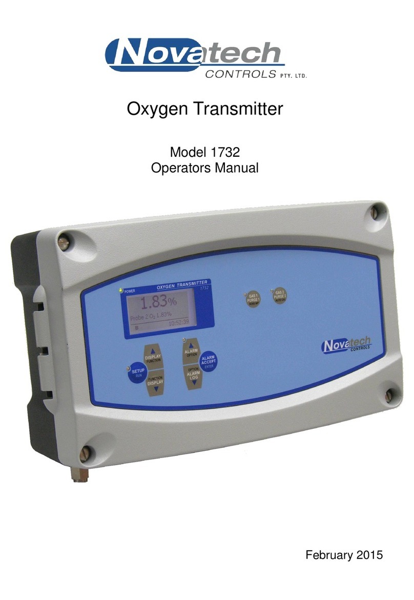
Novatech 1730 Series User manual

1730 Series Transmitter
Diagnostics Mode Reference Manual
Document Revision 1.03
Diagnostics Mode v1.08


Novatech Controls 1730 Series Diagnostics Mode Reference Manual
Document Revision 1.03 Page 1 of 16 Diagnostics Mode v1.08
What is Diagnostics Mode
The 1730 Series Transmitter is a microprocessor driven controller designed by Novatech Controls that
can be pre-loaded with several different firmware versions to suit various applications.
In standard operation the 1730 Series Transmitter runs a real-time operating system; a loop of
automated tasks which involve several highly inter-connected systems. Due to this closely integrated
nature, it can be difficult to isolate and diagnose specific hardware problems. For this reason, the
purpose of the Diagnostics Mode is to halt all other processes and isolate each particular piece of
hardware or specific sub-system so that it can be individually tested.
This reference manual covers the all aspects of the Diagnostics Mode, describes how the transmitter
should respond to various tests, and provide detailed technical advice on what may be the likely cause
of various fault conditions.
Finally it must be noted that fault diagnosis will often require a high level of electronic knowledge,
access to datasheets, schematics, various equipment including a digital multimeter (DMM), Multi-
function calibrator, and for some tests an oscilloscope. Repair may require access to replacement parts
and specialised equipment including surface-mount soldering equipment.
Please read the warnings and considerations below before continuing.
High Voltage Warning
In order to test the heater and purge/cal solid state relays (SSRs) the transmitter must
switch them on. This will only occur in the tests that are specifically required to test the
SSRs, and should only pulse the output for a maximum of 30ms each second. During this
time the outputs will be connected to live mains.
It is safe to leave oxygen probes connected during these tests, they will not be damaged or heat up
more than a few degrees. For testing the mains current feedback transformer it is actually required that
an oxygen probe is present.
Considerations Before Running the Diagnostics Mode
Be advised that while in Diagnostics Mode the transmitter will be offline and all standard
operations such as reading and re-transmitting of process variables will be stopped. It
may however for the purposes of testing still retransmit various signals over the 4-20mA
outputs, digital communications systems, energise the relay outputs, purge/cal solenoids
and heater power outputs.
Before you proceed if you have any control systems connected to the 1730 transmitter you should
disconnect these from the transmitter or consider what affect this may have if left connected.
NOTE: Before proceeding, please ensure you have read the relevant sections of the manual, have the
required electrical qualifications and have obtained any required authorization before proceeding.
Abbreviations Used Throughout this Manual
DMM –Digital Multimeter. Testing tool, supplied by the technician
MCU –Microprocessor. For the 1730 series transmitter this refers to component IC17, located
on the lower central part of the main board.

Novatech Controls 1730 Series Diagnostics Mode Reference Manual
Document Revision 1.03 Page 2 of 16 Diagnostics Mode v1.08
Entering Diagnostics Mode
To switch the transmitter to Diagnostics Mode you will need;
-Medium size flat head screwdriver to unscrew front case screws
-Small flat-head screw driver to change DIP switch position
Before continuing, disconnect power to the transmitter.
This should be done before opening the front case of the transmitter to eliminate the risk of electrical
shock.
After power has been disconnected, use the medium sized flat-head screwdriver to unscrew the four
screws on the front of the transmitter case. The screws are captive spring-loaded and will spring clear of
the base once fully unscrewed.
Open the case to reveal the inside electronics.
The lower left-hand side of the main PCB has a set of four DIP switches which can be accessed through a
hole in the shield (if fitted). It is not necessary to remove the EMI shield to access Diagnostics Mode,
however it may be required to remove the shield for further testing at a later stage.
While the transmitter is switched off, use a small flat-head screwdriver to move the bottom DIP switch
(labelled DIAG) to the right.
Re-connect power to the transmitter and switch on.
At this point, instead of displaying the Novatech logo and usual runtime information the display will say
‘Loading Diagnostics…’ with a version number on the second line. The version number indicates the
version of the Diagnostics Mode module compiled into the current EEPROM.
If the device powers up as described then you can skip the next chapter relating to power failure.
Total Power Failure
If the transmitter fails to power up when mains power is re-connected and switched on, you should
proceed to checking the mains circuitry for faults.
-Visually inspect the circuit board, mains power plug and mains power isolation switch SW2
checking that the connector wires and connectors are firmly inserted, and that SW2 is in the ON
position. Look for any blackened areas or scorch marks on the PCB or connectors that may
indicate a fault. Take particular note of the components marked VR3, VR4, VR5, VR6, VR7.
-Switch off the transmitter and remove the PCB fuse marked FS1 located adjacent to the main
AC-DC converter. If you find that this fuse is blown then it is very likely the Main AC-DC
converter block PS5 is damaged and will require replacement.
If PS5 is faulty it will cause FS1 to blow. If you replace blown FS1 without replacing faulty PS5 and
try switching the device back on you may notice the lights come on for about a second, then the
device going dead again as PS5 will immediately blow FS1.

Novatech Controls 1730 Series Diagnostics Mode Reference Manual
Document Revision 1.03 Page 3 of 16 Diagnostics Mode v1.08
Diagnostics Mode Keypad Interaction
The Diagnostics Mode consists of a series of numbered tests with user interaction being provided using
the local keypad and display.
Each individual test is designed to focus on a specific hardware component within the transmitter.
While some tests are fully automatic and non-interactive, others have several options that can be
adjusted by the operator using the keypad.
1. Function Up/Down –Change the test number
2. Option Up/Down –Change the test option
3. Enter –Toggle test option
The Option Up/Down and Enter keys perform different functions depending on the test. Please refer to
specific test application notes to see what keys are enabled for specific tests and their specific function
Pre Diagnostics Mode Tests
During the initialisation of Diagnostics Mode the transmitter performs two basic tests to confirm that
the display and keypad are functioning properly.
Testing the Display
On entering Diagnostics Mode the display test flashes a series of patterns on the display, and given that
there is no feedback to electronically confirm whether the display updated correctly it is up to the
technician to observe and determine whether the display is functioning properly.
The display test rapidly cycles through showing all pixels on, then all pixels off, then two patterns where
pixels alternate on or off. If the display contains any dead pixels, or if any regions are not updating
properly it should be immediately obvious to the technician.
The test can be repeated by power cycling the transmitter to restart Diagnostics Mode
Failure in this test would indicate a problem related to either the LCD module, the display PCB, or the
keypad/display bus buffers on the main PCB. In the majority of cases the solution would be to replace
the entire display PCB including the LCD module. It has also been observed that in some cases when
there has been voltage spiking on the mains, or if high voltage has been incorrectly applied to any of the
burner input or BFT inputs then the display bus buffer IC1 on the main PCB may be damaged.
On completion the transmitter immediately progresses to the second preliminary test.
1
2
3

Novatech Controls 1730 Series Diagnostics Mode Reference Manual
Document Revision 1.03 Page 4 of 16 Diagnostics Mode v1.08
Testing the Keypad
This second preliminary test will check the functionality of the interrupt driven hardware informing the
MCU when a key press is detected, as well as testing each of the physical buttons integrated into the
lexan on the front panel of the transmitter.
The transmitter will display the message ‘Press All Keys…’, and the technician should press each key on
the front panel one at a time. While being depressed, the display will indicate on the display which
button is being detected. Once all eight buttons have been individually pressed and released the
transmitter will progress to the numbered diagnostics mode tests.
The keypad inputs are transmitted to the main PCB along the same data bus as the display. Changes to
the keypad triggers an interrupt on the MCU, which causes the device to process the key press. If this
interrupt is not working properly then Diagnostics Mode will inform the technician of this fault. In this
case the keypad will continue to work in Diagnostics Mode, but will not work in the normal runtime
loop.
The cause of a keypad interrupt failure may be the SPI chip IC7 on the display PCB is damaged, or that
the transistor buffer TR1 (display PCB v1.0E and earlier) or NAND gate IC8 on the display PCB is
damaged. In either case, the easiest way to fix a keypad interrupt failure is to swap out the entire
display PCB and repeat the test.
Diagnostics Mode Tests
01. Reference Voltages Summary
Overview: This non-interactive test gives a summary of the three main voltage references as read by
the internal ADC.
Option Up/Down: no operation
Enter: no operation
The purpose of this test is to provide a quick overview of the three main ADC reference voltages as read
by the reference voltage feedback and calibration circuit. At a glance it may be possible to confirm
whether the ADC circuitry is working properly or requires further testing.
The display has a table with three rows and three columns. Each row shows the reference voltage, ADC
count number for the zero mV reference and the ADC count number for the span mV reference.
50mV
275 ± 75
3450 ± 645
200mV
275 ± 75
3450 ± 645
1200mV
275 ± 75
3450 ± 645
If all of the numbers on both the middle and right column read within tolerance then it can be safely
assumed that the voltage reference circuitry, analog channel selection circuitry, multiplexers, gain
circuitry and ADC chips are working correctly.
If any of the numbers are reading outside of the expected ranges, especially if any are reading 0 or 4095
then there is a problem with the analog circuitry.
Potential faults are the DC-DC isolated power supply PS4, the two voltage regulators IC11,IC27, the
voltage reference IC25, channel selection multiplexers IC8,IC9, gain op-amp IC14, gain select multiplexer
IC24, analog-digital converter IC23, or the analog switch IC7.

Novatech Controls 1730 Series Diagnostics Mode Reference Manual
Document Revision 1.03 Page 5 of 16 Diagnostics Mode v1.08
Before doing any more tests, check the four reference voltage test points on the main PCB (Ref 1.. Ref4)
and the two analog test points marked +12 & -12 above PS4 (relative to Acom)
The test point values should read:
Ideal Voltage
Min mV (-5%)
Max mV (+3%)
Ref1
47.2 mV
44.8 mV
48.7 mV
Ref2
189.1 mV
179.6 mV
194.8 mV
Ref3
1227 mV
1165.6 mV
1263.9 mV
Ref4
2500 mV
2375 mV
2575 mV
+12
12.0 V
11.4 V
12.6 V (±5%)
-12
-12.0 V
-11.4 V
-12.6 V (±5%)
In some cases where high voltage has damaged one or more components in the analog circuitry it is
possible that the damaged component may be drawing excess current and pulling the voltage
references and AVcc/AVee down. It may be necessary to systematically remove components one at a
time to identify the root cause of the problem.
The order for which the ICs are removed may depend on the history of the device. In some cases power
surges have been known to damage IC7, which in turn may damage IC25. Excess heat, or long service
life may cause PS4 to fail.
02. Reference 50mV
03. Reference 200mV
04. Reference 1200mV
05. Reference Zero
Overview: These four tests lock the analog multiplexer to the respective analog reference voltage
feedback channels. The MCU repeatedly samples the selected analog channel and displays the results
on the second line formatted in either raw ADC counts, or as an un-calibrated voltage.1
Option Up/Down: change the gain selection for the analog input.
Enter: no operation
The objective of these four tests it to confirm that the channel selection and gain select multiplexers are
working. To confirm that each channel is being selected the technician can is a DMM to measure the
differential voltage between the two test points on the PCB marked M+ and M-. If the channel selection
is working properly then the voltage measured between these two test points should be very close to
the same voltage measured between the selected reference test point and ground.
If the voltage differential does not match this voltage then there is a problem with the channel selection
circuitry. The problem may be that one of the channel selection multiplexers IC8 or IC9 is not working,
or possibly that the channel selection I/O lines between the MCU and the IC8/IC9 are not working. The
procedure for troubleshooting would be to check the port lines P8-0..2 are functioning, which may
require removing IC8/IC9. If they are working then IC8/IC9 should be replaced.
1Un-calibrated meaning that default calibration values are used in the calculation of the voltage. The voltage
displayed should be accurate to within ±2%, any slight inaccuracy should not be taken as an indication of hardware
fault.

Novatech Controls 1730 Series Diagnostics Mode Reference Manual
Document Revision 1.03 Page 6 of 16 Diagnostics Mode v1.08
To test the gain circuitry the technician can change the gain using the option up/down keys. The gain
multiplexer IC24 changes the feedback resistor for one of the op-amp channels on IC14, resulting in four
possible gain ranges for the analog signal into the ADC. The objective is that each reference voltage will
have one optimal gain range to amplify the analog voltage to approximately 85% of the analog
The gain for each of the gain selection channels are as follows:
Range
Physical Gain
Saturation Voltage
0
40.7
57.5mV
1
10.4
225.4mV
2
1.75
1334.3mV
3
1
2338.4mV
Not all gain ranges are available for all of the reference voltages, as higher gains will immediately
saturate the analog signal for the higher reference voltages. It is however possible to apply lower gains
to the lower reference channels to confirm that the gain selection is working.
If the gain selection is not working then the problem may be the gain selection multiplexer IC24, the op-
amp IC14, or possibly the gain selection I/O lines from the MCU pins P8-3..4. The procedure for
troubleshooting would be to check the I/O lines to the multiplexer are working, and then replace IC14
followed by IC24.
06. Probe 1 Temperature Input Channel
07. Probe 1 EMF Input Channel
08. Probe 2 Temperature Input Channel
09. Probe 2 EMF Input Channel
Overview: These four tests lock the analog multiplexer to the respective analog input channels. The
MCU repeatedly samples the selected analog channel and displays the results on the second line
formatted in either raw ADC counts, or as an un-calibrated voltage.2
Option Up/Down: change the gain selection for the analog input.
Enter: no operation
The objective of these four tests it to confirm that the hardware specific to the off-board analog inputs
is working. Before performing these tests it is important to confirm first that the analog input selection
and gain circuitry is working by performing diagnostics tests 02 through to 05 on the previous page.
The process is identical to the previous tests for checking the reference voltages; the channels selected
however correspond to the four analog inputs on the terminals used for oxygen EMF and temperature.
To test these channels it is necessary to have some sort of calibrated source generator connected to the
channel being tested.
For testing the temperature input channels, the signal source must be capable of simulating a K-type
thermocouple, cold junction compensated signal in the range of -50°C to 1500°C.
2Un-calibrated meaning that default calibration values are used in the calculation of the voltage. The voltage
displayed should be accurate to within ±2%, any slight inaccuracy should not be taken as an indication of hardware
fault.

Novatech Controls 1730 Series Diagnostics Mode Reference Manual
Document Revision 1.03 Page 7 of 16 Diagnostics Mode v1.08
For testing the probe EMF input channels, the signal source must be capable of sending a DC voltage
signal in the range of -50mV to 2000mV.
NOTE: Signals outside of the range of -50mV to 2400mV may damage the analog input circuitry.
By modulating the output from the signal generator, the transmitter should be able to quickly and
accurately reflect the voltage or temperature changes on the second line of the display.
Failure to reflect these changes would indicate some fault between the input terminals and the channel
selection multiplexer components IC8/IC9. This may be caused by broken solder joints, damaged tracks
or ancillary components such as pull-up resistors.
Both of the temperature inputs have pull-up resistors that will cause the signal to read 1371.1°C if they
are open-circuit.
10. Ambient Temperature Sensor
Overview: The transmitter has a solid-state temperature sensor IC4 that is used to monitor case
temperature and for thermocouple cold-junction compensation. The sensor is located in the top-left
corner of the main PCB directly above the input terminals for probe #1, the analog output signal is sent
directly to the MCU.
Option Up/Down: no operation
Enter: no operation
The display should indicate ambient temperature in degrees Celsius. It should read close to room
temperature, possibly a couple of degrees higher due to heat dissipated from the transmitter circuitry.
To confirm the sensor is live reading temperature, try to warm it by touching it lightly with a finger, or
cooling it using air from a can.
The output from the temperature sensor can be read using a DMM as a DC signal via the unmarked test-
point directly adjacent to IC4. The component is a Texas Instruments LM50, which should output an
analog signal of 500mV offset plus 10mV/°C. For example at 25°C the signal should be (500mV +
25x10mV = 750mV)
The order for testing this sensor would be to confirm that the component IC4 is working using a DMM
on the unmarked adjacent test-point, then check whether the signal is being transmitted to MCU pin
P10_0.
11. Ambient RH Sensor
Overview: The transmitter has a solid-state relative humidity sensor IC30 that is used for oxygen
calculations. The sensor is located in the top-left corner of the main PCB above the analog input
circuitry. The analog signal is buffered via an op-amp IC31 and attenuated using two resistors, this
signal is sent directly to the MCU.
Option Up/Down: no operation
Enter: no operation
The display should show ambient air relative humidity as percentage. The reading will vary depending
on the ambient conditions.
The output from the humidity sensor can be read using a DMM as a DC signal via the unmarked test-
point directly adjacent to IC30. The component is a Honeywell HIH-4000-002, which outputs a linearised
voltage of ~825mV @ 0% RH through to ~3.75V @ 100% RH. The signal is sent to the MCU via op-amp
IC31 to buffer the signal and R127 & R128 that attenuate the signal by 50%.

Novatech Controls 1730 Series Diagnostics Mode Reference Manual
Document Revision 1.03 Page 8 of 16 Diagnostics Mode v1.08
The order for troubleshooting this sensor would be to confirm that the component IC31 is working using
a DMM on the unmarked adjacent test-point, then to check the output of op-amp IC31 at each of the
output pins, then check whether the signal is being transmitter to MCU pi P10_5.
12. Reference Air Pump Current
Overview: The reference air pump drive circuitry is designed to power a small DC pump using a
controlled digital pulse. This allows the MCU to adjust the speed of the pump by modulating the output
voltage. The circuit is designed to provide a continuous current of ~100mA, with a maximum continuous
current of ~250mA. The drive circuitry has integrated load detection that is used to monitor current
usage so that the MCU can switch the pump off if the output is overloaded to prevent damage to the
drive circuitry.
Option Up/Down: increase/decrease the digital PWM pulse (pump voltage)
Enter: no operation
The display indicates both PWM (pulse with modulation) output level in percentage, as well as current
detected using the feedback system. There are in effect two symbiotic systems being tested at once;
the pump drive voltage and the current feedback system. In standard operation the pump should start
turning once the PWM level reaches a certain level, the current should also rise according to use.
It is noted that with some pumps, when the motor sticks the pump can draw considerable current.
To test the PWM output and pump voltage, remove the reference air pump and use a DMM to measure
the DC voltage across the ref pump output terminals. Use the option keys to change the PWM output
and observe the changes to the voltage displayed on the DMM. The voltage should follow a linear path
from ~0V @ 0% PWM, saturating at ~5V @ ~85% PWM output.
If the voltage on the ref pump output terminals does not respond as described when changing the PWM
output, use an oscilloscope to check the trace at test-point P1, located adjacent to R110. The trace
should show a digital pulse with a mark to space ratio corresponding to the PWM output. This trace is
input into an op-amp IC29 which drives the transistor TR9. If the digital trace is present, but no
corresponding voltage, replace TR9, test again, replace IC29 if still not working.
To test the current feedback there are several methods. The easiest option would be to use a known
working CM-15 reference air pump as supplied by Novatech. With the PWM output set to 100% the
pump should run with a smooth cadence and draw a continuous current of ~60mA. Another way to test
this would be to place a 1/4w 100 ohm resistor between the ref air pump terminals. The current drawn
should also display ~50mA @ 100% PWM.
0
1
2
3
4
5
0 25 50 75 100
Ref Pump Output V
PWM Outout %

Novatech Controls 1730 Series Diagnostics Mode Reference Manual
Document Revision 1.03 Page 9 of 16 Diagnostics Mode v1.08
If the voltage output is working and current feedback is not working then check the output from the op-
amp IC29, and check MCU pin P10_1.
13. Mains Detection
Warning: This test requires a heated probe to be connected to the Heater 1 output, and
will involve switching on mains power to this probe in short bursts.
Overview: Mains detection is achieved by measuring the AC current used to power the heated probe.
The transmitter measures frequency by detecting the zero crossover points of the alternating current
signal, and it calculates voltage by assuming the known impedance of the probe heater. This
assumption is easily invalidated if the device attached to Heater 1 is not a Novatech Controls supplied
model 1231 or 1234 heated probe.
Note: To enable mains power output to Probe 1 a link must be inserted between the burner input
terminals 10 &11 creating a short-circuit.
Option Up/Down: no operation
Enter: no operation
With the probe plugged into Heater 1 output and the burner input link present the transmitter should
be able to immediately detect a mains voltage and frequency.
Also note, if mains cannot be detected, first check the fuses FS2 and FS3 are not open-circuit.
If the feedback circuit is giving incorrect results then the transmitter current transformer T1 or gain
resistor R108 may be damaged. Given that the current transformers used are made to order for this
specific application, it may be difficult to obtain suitable replacements. The board may need to be
returned to Novatech Controls for repair.
If there is a fault with the mains detection circuitry then it is possible to override automatic mains
detection using options in the Calibration Menu, allowing the transmitter to continue operating.
Mains detection is also used during runtime to monitor the switching of the solid-state relay (SSR) that
regulates the probe temperature. If mains detection is not working then it is quite possible that the SSR
short-circuit protection is also not working. In this scenario, if a SSR fails short-circuit this fault may not
be detected by the analyser resulting in the probe being irreparably damaged.
14. SSR Relay Tests
Warning: This test requires a mains powered load to be connected to each of the four
relay outputs in order. It will involve switching on mains power to each of the outputs in
short bursts.
Overview: The transmitter contains four solid-state relays (SSRs), namely the two heater outputs and
the two purge/cal control relays. The four SSR outputs also have an electromechanical relay RL3 that is
used to isolate the mains voltage from the four SSRs. This test can be used to individually switch each
SSR and displays the ADC feedback from the current sensing circuit in raw counts.
Option Up/Down: next/previous relay
Enter: no operation
The current detection circuit measures the total AC load across all of the SSR outputs. This test is
designed to show how this load changes when each of the relays is pulsed. It can help to confirm that
the burner relay, an electromechanical relay RL3 is functioning and whether any of the four solid-state

Novatech Controls 1730 Series Diagnostics Mode Reference Manual
Document Revision 1.03 Page 10 of 16 Diagnostics Mode v1.08
relays have failed short-circuit. Finally it also confirms that the current transformer and feedback circuit
is working.
Note: To enable mains power output to Probe 1 a link must be inserted between the burner input
terminals 10&11 creating a short-circuit. The electromechanical relay RL3 cannot be energised without
this link being present.
The first test should be to check using a DMM whether there is any mains present on any of the four
output terminals with the burner relay is off. To switch off the burner relay press the option keys until
the display says ‘Burner Relay Off’, and when selecting this option it should be possible to hear the
contacts in the mechanical relay changing. With the burner relay off the terminals should be physically
isolated from mains, if there is any mains on the outputs with the burner off then the electromechanical
relay RL3 has failed.
The next test is to confirm that each of the solid-state relays in turn can switch mains voltage both on
and off. To test that none of the SSR have failed short-circuit, use the option keys to set the transmitter
to ‘All SSRs off’. In this position, RL3 is energised, all SSRs should be off. Plug the probe into each output
in turn and observe the ‘mA counts’ line. A normal number for no load should be ~8 counts. If this
number is significantly higher, or if plugging the heater into any one of the outputs causes this to rise
then this would be an indication that the SSR being tested has shorted.
Lastly, plug the heater into each output in turn and use the option key to enable the selected output.
While doing this observe the mA counts, which should rise to ~140 counts when switched on to indicate
that it is sensing the load of the probe heater. If this does not happen then either the SSR has failed
open-circuit, or there is a problem with the current detection circuit.
To identify whether the SSR or the current detection circuit that has failed will require some sort of
physical load that can be observed whether it is being switched on or off, such as a mains voltage neon
indicator. If the problem is with the detection circuit then it is likely the device will need to be returned
to Novatech Controls for repair.
15. BFT Analog Input
Overview: The BFT is an analog input located near the bottom-left corner of the main PCB. It is used for
some applications for ancillary readings such as measuring process pressure. The BFT measures a DC
signal in the range of 0-2500mV. Testing will require the use of a source generator capable of
outputting voltage in this range.
Option Up/Down: no operation
Enter: no operation
With the BFT open circuit, there is some internal pull-up circuitry that will hold the BFT input at some
level for PCB version 1.2 Rev G and older. This level varies slightly, but should be ~635mV. Starting with
PCB version 1.2 Rev H and newer the BFT will drop to 0mV when open circuit.
Connect an external signal generator to the BFT input and check that the voltage output from the
generator matches the display. If there is a fault then check the track between the terminal and MCU
pin P10_4.
Test input range 0-2400mV with LK2 open, the display should match the signal generator. Secondly,
place a short across LK2 and use the signal generator to test the input range 0-20mA. LK2 will place a
120 ohm resister across the terminals, so the voltage on the display should be 120x Input mA.

Novatech Controls 1730 Series Diagnostics Mode Reference Manual
Document Revision 1.03 Page 11 of 16 Diagnostics Mode v1.08
If there is any non-linearity while testing current with LK2 shorted, consider removing Zener diode D14
as this is the cause of any linearization problem. Some newer firmware versions include software
linearization to remove the affect of D14, however it is far easier to fix this problem with hardware.
16. 4-20mA Output 1 Calibration Test
17. 4-20mA Output 2 Calibration Test
Overview: This is a non-interactive test that can show at a simple glance whether both the 4-20mA
output circuitry and internal calibration feedback circuitry is working.
Option Up/Down: repeat the test
Enter: no operation
The 1730 transmitter has two isolated 4-20mA output channels. For testing purposes the transmitter is
capable of re-routing the output from terminals using an electromechanical relay through a fixed load
resistor and back into one of the analog inputs on the MCU. When you enter this menu, or press one of
the option keys to repeat the test, the transmitter redirects the analog input and performs a series of
automatic tests on the respective isolated 4-20mA output channel and displays the results on the
screen.
The first test involves automatically setting the output to ~4mA and reading the return signal on the ADC
in raw counts. This first reading is displayed after the word ‘Zero’ and should be in the range of
11000±7000 counts. Typically this number is ~10300.
Next the device automatically sets the output to ~20mA and reads the return signal on the ADC in raw
counts. This second reading is displayed after the word ‘Span’ and should be in the range of
43000±3000 counts. Typically this number is ~43000.
The third line will either say ‘Output OK’, ‘WARNING’ or ‘FAIL’ depending on whether the Zero and Span
numbers are within expected tolerances. If this line says ‘Output OK’ then it is safe to assume the
output is working. If the automatic testing fails then either the output circuitry is damaged, or the
feedback circuitry has failed.
If the feedback circuitry has failed then it is still possible to use the output once it has been manually
calibrated. Refer to the device Technical Manual for further information. Continue reading the next to
Diagnostic tests for information on how to determine the specific point of failure of the analog output.
18. 4-20mA Output 1 DAC Test
19. 4-20mA Output 2 DAC Test
Overview: These two tests follow on from Diagnostics test #16 & #17 and allow a more comprehensive
set of options for a technician to diagnose the specific point of failure for the two isolated analog
outputs. These tests allows each of the 4-20mA analog output channels to be manually set to specific
levels, and manipulate the cal feedback relay.
Option Up/Down: increase/decrease the 4-20mA output level as a percentage of full scale
Enter: toggle the feedback relay on or off
The two 4-20mA output channels on the 1730 transmitter have dedicated isolated hardware to convert
a 16-bit signal from the MCU into a proportional analog output. This output signal can be switched via a
feedback relay through a fixed load resistor and read by the MCU as part of the self diagnostics process,
although doing so un-couples the outputs from the terminals. The transmitter cannot monitor the
outputs during standard operation, only during calibration or diagnostics.

Novatech Controls 1730 Series Diagnostics Mode Reference Manual
Document Revision 1.03 Page 12 of 16 Diagnostics Mode v1.08
By using the option keys, the output level can be set as a percentage of full scale at ~25mA. Pressing the
enter key toggles the feedback resistor, which allows the technician to read the output either on the
terminals on the PCB, or via the feedback to the MCU.
In standard operation, with the cal feedback enabled, the transmitter should read ~0mA @ 0%, ~12.7mA
@ 50% and ~25mA @ 100% output, with the output current tracking a linear path between these
points.
If the outputs are not tracking as described then the first thing to check should be the analog voltage
reference points next to the DC-DC converter for the channel in question. For channel 1 this is the three
test-points labelled D1com,+12,-12 adjacent to PS3, for channel 2 this is the test-points labelled
D2com,+12,-12 adjacent to PS2. If these test points are reading correct voltages then the next thing to
test is the output terminals DMM to confirm whether the problem is with the output drive circuitry, or
the cal feedback circuitry.
Set the cal feedback to disabled, and using the DMM, check whether the analog signal can be seen on
the output terminals on the PCB. If the outputs are working, but the cal feedback is not then there is a
problem with the cal feedback. Check the cal feedback relay RL1/RL2 is switching, whether there is an
analog signal on the load resistor R27, and finally check the track between R27 and the MCU pin P10_3.
If the output is not registering an analog signal when the cal feedback is both on and off then the
problem is likely with the output drive circuitry.
The two outputs have test points, labelled D1 and D2 which are located on the PCB next to the output
power transistor TR4/TR5. Relative to the isolated digital common labelled D1com and D2com adjacent
to the respective DC-DC converter, these analog test points should give an analog signal linearly
proportional to the output level percentage. It should be scaled 0mV @ 0% output and 2500mV @
100% output, tracking a linear path for each step change between these two points. If this analog signal
is present then skip the next paragraph regarding the oscilloscope.
Using an oscilloscope, check the output signal from the MCU pin P7_4 for channel 1, pin P7_6 for
channel 2. An easy test point can be found on the resistor right before the optocouple OP5/OP6. A
digital signal with a variable mark to space ratio should be seen. This mark to space ratio should change
when the option keys are used to increase and decrease the output level percentage. If this signal is
present, next check the output of the optocouple. If the optocouple is working and there is no analog
signal on the D1/D2 test point then replace the transistor TR6/TR7 and voltage reference IC15/IC16
components as required.
0.0
4.0
8.0
12.0
16.0
20.0
24.0
0% 10% 20% 30% 40% 50% 60% 70% 80% 90% 100%
Feedback Current mA
Channel Digital Output Level

Novatech Controls 1730 Series Diagnostics Mode Reference Manual
Document Revision 1.03 Page 13 of 16 Diagnostics Mode v1.08
If there is an analog signal at D1/D2, but not on the output then the problem is likely to be the power
transistor TR4/TR5 or the op-amp IC12/IC13. Check also that the light emitting diode LED4/LED5 is
working and that the legs of the LED have not become twisted inside the long standoff.
20. Digital Inputs
Overview: The digital inputs being tested include the four inputs from the dip-switch SW1, the 0.1”
jumper SW5 and the two inputs on the terminals marked ‘Flow SW’ and ‘Burner Input’.
Option Up/Down: no operation
Enter: no operation
To test each of the dip-switch inputs, toggle them each individually and confirm that the display changes
to reflect a change in the physical state. If any of these digital inputs do not work as expected then try
manually shorting the associated pins on the IC using a small piece of wire to test whether the dip-
switch is damaged. Check the tracks going back to the MCU for damage.
To check SW5 use a small jumper to short the pins, observing the state change on the display
accordingly. If this does not work as expected then check the track to the MUC pin P2_6.
To check the Flow SW and burner input use a small terminal connector to short the terminal input pins
16 & 17 for the Purge Flow Switch, and terminal input pins 10 & 11 for the burner input.
If these digital inputs fail to work as expected, check the associated circuitry and tracks to the MCU.
Both inputs have a transistor between the input and the MCU for protection. The burner input also has
two micro-fuses in series with each pin and a transient voltage suppressor across the terminals for
additional protection. If any of these devices are damaged then consider the cause for this damage
while replacing the damaged components.
21. Alarm Relays
Overview: The 1730 series has four mains-power rated alarm relays that can be programmed to
perform various functions. Each of these relays is independently controlled via the MCU. This test
individually energises each relay allowing the contacts to be tested using a DMM
Option Up/Down: select next/previous relay
Enter: no operation
As each relay is selected the relay solenoid is energised and the two terminals corresponding to that
relay should be shorted. Use a DMM to check continuity between the terminals and check that they
make a continuous circuit when the relay is energised and open circuit when the relay is de-energised.
If any of the relays fail to operate as expected, check the trace from the MCU to the transistorT10-T13
for the correct signal, then replace the relay and transistor as required.
22. LED Test –Lexan and Main PCB
Option Up/Down: select next/previous relay
Enter: no operation
This test is used to check that all the LEDs that are built into the lexan on the front of the case work, and
that the RS485 LED on the main PCB works. Cycling through each of the LEDs using the option keys
should enable each selected LED in turn to confirm that they work.
Option Up/Down: select next/previous LED
Enter: no operation

Novatech Controls 1730 Series Diagnostics Mode Reference Manual
Document Revision 1.03 Page 14 of 16 Diagnostics Mode v1.08
If any of the lexan LEDs are not working then check the signal on the flexible cable between the display
PCB and the lexan. The lexan itself is unserviceable, so any failed LEDs would require the replacement
of the lexan label.
23. LCD Backlight
Overview: The backlight on the LCD display can be enabled and disabled from the MCU. This test can
check what state the backlight is in, and whether it is functioning properly.
Option Up/Down: toggle the backlight on/off
Enter: no operation
If the backlight is not working then the LCD module will need replacing. The LCD module itself can be
replaced individually. Alternatively the whole display circuit board with LCD module can be ordered as a
complete assembly allowing for simple swap-out replacement.
24. RS232 Port
Overview: This non-interactive test allows for simple automated testing of the RS-232 serial
communications on the transmitter. To test the RS-232 port place a jumper between terminal pins 18 &
19 –RS-232 Tx and RS-232 Rx.
Option Up/Down: no operation
Enter: no operation
The serial port continuously transmits a string of characters, while simultaneously listening for a
response. By placing a loop between the Tx and Rx terminals the device will continuously receive the
string of characters that it transmits therefore confirming that both transmit and receive are working.
If both transmit and receive are working the words ‘Loopback ON’ will appear on the display. If these
words do not appear when there is a short between terminals then there is a problem with the Tx or Rx
circuitry.
Before testing any of the serial port circuitry, first check the voltage test-points located adjacent to PS1
marked SGnd,+12,-12. On the newer boards there is also a +5 test point added. Confirm that each of
the test points measure the correct voltage with respect to SGnd.
Testing for serial port problems will require tracing the signal output from the MCU using an
oscilloscope. The testing itself is broken down into testing the Tx circuitry first, then if it can be seen
that this works, test the Rx circuitry second.
The first test should be to observe the Tx and Rx and 485 LEDs. During this test, the 485 LED should be
off. If the 485 LED is on then check the track between resistor R38 and the MCU pin P2_4.
If the Rx LED is on when the loopback jumper is OFF then there is a problem with either the logic chips
IC18, IC19, or the optocouple OP4. Using a DMM, check some of the states of the pins. If IC18_9 and
IC18_10 are high and IC18_8 is low then likely it is not IC18. If IC19_3 is high and IC19_4 is low then
replace OP4.
With the loopback jumper OFF the Tx LED should give a short flash every second and the Rx LED should
stay off. If the Tx LED is not flashing then this suggests that the signal from the MCU is not getting as far
as the LED. Use an oscilloscope to trace the signal through OP3 and IC10 to find the problem, also
confirming that the Tx LED is working and does not have twisted legs inside the standoff.

Novatech Controls 1730 Series Diagnostics Mode Reference Manual
Document Revision 1.03 Page 15 of 16 Diagnostics Mode v1.08
Once the Tx LED is flashing, use the oscilloscope to test the signal on the Tx terminal #18. If you can see
the Tx LED flashing, and the signal on the Tx terminal then move on to testing the Rx circuitry. Place the
loopback jumper between the Tx and Rx terminals to continue testing.
With the loopback on the Rx LED and the Tx LED should flash on together each second. If the Rx LED is
not flashing, use the oscilloscope to test where the signal stops working by tracing it through IC10 OP4,
then IC18 & IC19 logic gates.
25. RS485 Port
Overview: These tests are designed to check the functionality of the RS485 port by individually toggling
different port lines used by the RS485 hardware. The quickest way to confirm whether the RS-485 port
is working is to configure the port for use using runtime and try polling the device using the simple
Modbus Master PC Software available to download on the Novatech Controls website. If this suggests
that there is a problem then this diagnostic test can be used to assist in isolating the problem.
Option Up/Down: toggle different port line
Enter: no operation
By toggling each port line individually it is possible using an oscilloscope to trace the oscillating signals
one at a time through each logic gate and optical component to confirm whether they are working. The
option to toggle P6_0 is used to confirm OP1 is working. The option to toggle P6_3 is used to confirm
OP2 is working by shorting the Tx and Rx pins on IC6. To test OP3 use the automatic process for testing
the RS232 port from the previous test. If all three optocouples OP1, OP2 & OP3 are shown to be
working, replace IC6.
26. EEPROM & BBRAM
Overview: This is a non-interactive test that displays the status of the three main non-volatile storage
devices present on the transmitter. It tests whether the device is present and can be successfully read.
Option Up/Down: no operation
Enter: no operation
The first item is the iButton memory device labelled RTC located on the bottom centre of the main PCB.
This device may register as either a DS1904 or DS1994 depending on when it was commissioned. If this
device fails then the real-time clock and associated timed events may fail to work properly
The second item M24512 is a flash memory component IC29 that stores all of the device calibration and
configuration. If this device fails then the transmitter will factory reset every time it is switched on.
The third item labelled AM29F010 refers to the firmware upgrade socket. It is normal for this test to fail
unless a properly programmed upgrade EEPROM is plugged into this socket. It is also not necessary for
this socket to work for standard runtime operation; only when updating the on-board firmware.
27. Watchdog Timer
Overview: This tests the internal watchdog timer in the device. If the watchdog timer works then the
device should automatically reset approximately 200 milliseconds after pressing one of the option keys
to commence the test.
Option Up/Down: commence testing the watchdog timer
Enter: no operation
The device will reset, this is the purpose of the watchdog timer. If the device resets then this test has
passed. If the device does not reset then contact Novatech Controls to discuss options.

Novatech Controls 1730 Series Diagnostics Mode Reference Manual
Document Revision 1.03 Page 16 of 16 Diagnostics Mode v1.08
28. ADC Calibration
This option is not currently used for testing.

1
1
2
2
3
3
4
4
5
5
6
6
7
7
8
8
D D
C C
B B
A A
Title
Number RevisionSize
A3
Date: 26/02/2016 Sheet of
File: J:\Projects------------\..\1732-1 Master.SchDocDrawn By:
AI+-[0..3]
AI--[0..3]
4-20out#2+
4-20out#2-
P1-[0..7]
P4-[0..7]
P7-[0..7]
P8-[0..7]
P9-[0..7]
P10-[0..7]
4-20out#1+
4-20out#1-
P2-[0..7]
Analog
1732-3 Analog Sch.sch
RS232-Rx
RS232-Tx
RS485-
RS485+
P0-[0..7]
P1-[0..7]
P4-[0..7]
P6-[0..7]
P7-[0..7]
P5-[0..7]
CNVss
Reset
P2-[0..7]
Serial digital
1732-4 SerDig Sch.sch
1
2
3
4
CN10
1
2
CN13
1
2
3
4
CN2
1
2
3
4
5
CN5
1
2
3
CN11
P0-[0..7]
P1-[0..7]
P2-[0..7]
P3-[0..7]
P4-[0..7]
P5-[0..7]
P6-[0..7]
P7-[0..7]
P8-[0..7]
P9-[0..7]
P10-[0..7]
Reset
CNVss
Micro
1732-2 Micro Sch.sch
R124 4k7
TR11
D10
P3-3
R9 10M
R10 10M R29 10k
R20 10M
1
2
3
4
5
6
7
8
CN9
R2 120R
Sensor 1 + 1
Sensor 1 - 2
Thermocouple 1 + 3
Thermocouple 1 - 4
Sensor2 + 5
Sensor2 - 6
+5v 9
Output #1+ 12
Output #1- 13
Burner input 10
Burner input 11
Network + 21
Network - 20
Network Com 22
39 Cal / Purge 2
40 Cal / Purge 1
38 Solenoid Com
26 Common alarm relay
27 Common alarm relay
29 Process alarm relay 1
30 Process alarm relay 2
44 Heater 1
43 Heater 1
37 Mains A
36 Mains N
34 Earth
R121 4k7
D9
TR10
Gnd
Gnd
P5-[0..7]
P3-2
Vcc
SSR4
SSR1
SSR2
R114 470R
R112 470R
R111 470R
R102 1k
R100 1k
R99
1k
LED8
LED7
LED10
P3-0
P3-6
P3-7
FS2
FS3
Mains A
Mains N
V+
V-
Earth
V+
V-
PS5
Power supply ArchAPC-10S
Gnd
RS232 Rx 18
RS232 Tx 19 RS232-Tx
RS232-Rx
RS485+
RS485-
D3
BAV99
Gnd
Gnd
RL3
Vcc
TR8
R98
470R
R97
10k
P9-[0..7]
P9-7
D7
AI+-[0..3]
AI--[0..3]
4-20out#1+
4-20out#1-
AI+-0
AI+-2
AI--1
D8
T1R109
10k
R108 100R
Gnd
C58
0.1
P0-[0..7]
P1-[0..7]
P2-[0..7]
P3-[0..7]
P4-[0..7]
P7-[0..7]
P8-[0..7]
P6-[0..7]
P10-[0..7]
1
2
CN8
R117 680R
R120 12k
R116 150RGnd
Vcc
Gnd
Pump +
Pump -
R115 1R
5
6
7IC29B
LM358
R106 5k6
R107 1k
C56
10uF/16v Electro
Gnd
P10-1
P7-2
3
2
1
84
IC29A
LM358
Gnd
Vcc
R119 10k
C60
10uF/16v Electro
P1-4
T +
-
IC4
LM50 SMD
Gnd
Vcc
P10-0
P10-2
R110 10k
C59
1uF/16V Tant
Gnd
TR9
BD140
Power
1
2
3
4
5
6
CN6
Output #2+ 14
Output #2- 15
4-20out#2+
4-20out#2-
1
2
3
4
5
6
7
CN3
Aux TC 2 + 7
Aux TC 2 - 8 AI--3
Purge flow switch 16
Purge flow switch 17
LK1
P5-6
R1 10M
28 Process alarm relay 1
35
Out
4
Out
3
In 1
In 2
FL1
RL4
RL5
SW2
1
2
CN12
41 Heater 2
42 Heater 2
LED6
R8 1k
Burner ON
Test Point +5V
Test Point Dig Common
R125 0R
LED11
R1181k
Pump power
Gnd P2-7
Vcc
Gnd
SGnd
AVee
Vcc
Version 1.2 GMaster, power and terminals
Novatech Controls
1 4
1
2
3
CN4
GND
AVcc
P10-4
+12 V 23
BFT+ 24
BFT- 25
P2-6
LK5
Gnd
Auxilliary link
C65
10uF/16v Tant
R122 4k7
TR12
D11 RL6
Vcc
Gnd
P3-4 31 Process alarm relay 2
FS1
SSR3
R113 470R
R101 1k
LED9
P3-1
R35
10M
CNVss
Reset
C1
0.1
D1
BAV99
R36
10k
R34
120R
AVcc
LK2
Gnd
RL7
TR13
R123 4k7
D12
32 Process alarm relay 3
33 Process alarm relay 3
Gnd
P3-5
Test point P1
P10-5
C66
0.1 Gnd
RH +
-
IC30
HIH-4000-002
R126 470R
LED12
LED SMD Green
Vcc
3
2
1
8 4
LM358
IC31A
5
6
7
LM358
IC31B
R127 10k
R128 10k
AVcc(5)
AVee(5)
C67
0.1
Gnd
RelayNC1
RelayNC2
POWER
B32022A3103M Y2
C68
0.01uF
C69
B32922C3333K X2
C70
0.033uF
TS1
Transorb-DC
VR1VR2
VR3
VR4
VR5
VR6
VR7
1730 Series Analyser
C3
0.1
FS4
LittelFuse 200mA Quick Blow
FS5
TS2
1.5KE6.8A
R130
2k7
TR14
R129
2k7
Vcc
R131
10k
Gnd
C2
0.1
R132 2k7
Vcc
R133 2k7
TR15
R37
10k
Gnd
R134 10k
D14
3.3V 300mW Zener
Gnd

1
1
2
2
3
3
4
4
5
5
6
6
7
7
8
8
D D
C C
B B
A A
Title
Number RevisionSize
A3
Date: 26/02/2016 Sheet of
File: J:\Projects------------\..\1732-3 Analog Sch.SchDrawn By:
014
15
26
12
3
11
1
13
4
10
2
Vcc
16
Gnd
8315
Vee
90123
/En
7
IC7
74HC4316 SMD
R41 6k8
R30
1k
R42 1k
R28 10k
AVcc(5)
AVee(5)
Gnd
P2-2
P2-0
P2-1
Vref
1
+in
2
-in
3
Gnd
4
/CS 5
Dout 6
CLK 7
Vcc 8
LTC1286CS8
IC23
10
9
8
IC14C
OPA4234UA
12
13
14
IC14D
OPA4234UA
5
6
7
IC14B
OPA4234UA
3
2
1
411
IC14A
OPA4234UA
Gnd
AVcc(5)
R6010k
R5910k
R7410k
R72 10k
R73
1k
R85
6k8
R83 270k
R84 1k
R82
1k5
AVcc
Gnd
C31 0.01uF
C34 0.01uF
AVee
Gnd
C32
0.01uF
R51 1k
R52 1k
C17
0.001uF
C16 0.001uF
Gnd
Gnd
C51
0.1
C4
0.1
Gnd
Gnd
C28
0.01uF
Gnd
Gnd
R96 22k
R89 330k
X0
13
X1
14
X2
15
X3
12
X4
1
X5
5
X6
2
X7
4
INH 6
A11
B10
C9
VEE 7
X3
VCC 16
GND 8
IC24 CD4051
Gnd
Gnd
Gnd
AVee(5)
P8-[0..7]
AVcc(5)
X0
13
X1
14
X2
15
X3
12
X4
1
X5
5
X6
2
X7
4
INH 6
A11
B10
C9
VEE 7
X3
VCC 16
GND 8
IC8
CD4051
Gnd
Gnd
X0
13
X1
14
X2
15
X3
12
X4
1
X5
5
X6
2
X7
4
INH 6
A11
B10
C9
VEE 7
X3
VCC 16
GND 8
IC9
CD4051
AVee(5)
AVee(5)
AVcc(5)
AVcc(5)
R19100k
R15
100k
R18100k
R14100k
R17100k
R13100k
R12
100k
R16100k
C120.1
C110.1
C240.1
C220.1
C230.1
C13
1uF/16v Tant
C90.1
C210.1
C50.1
C60.1
C70.1
C8
Gnd
Gnd
C10
0.1
Gnd
P8-3
P8-4
R79 470RR80 6K8
Gnd
IC22
Gnd
R81 4K7
AVee
P9-[0..7]
P9-0
P8-0
P8-1
P8-2
P8-[0..7]
P9-1
P9-2
R93 27k
R94 2k2
R90 1k
Gnd
R91 3k01
46mV
180mV
ADC RefV 2
ADC RefV 1
Test Point ADC Ref Com
ADC RefV 3
1200mV
R92 22k
2500mV
AVcc
P8-0
P8-1
P8-2
AI--[0..3]
AI+-[0..3] AI+-[0..3]
AI--[0..3]
AI+-0
AI--1
AI+-2
ADCRef
ADCRef
IC15
LM336-2.5 SMD
R68
4k7
R69
10k
R86
1K
R65
27k
C18
10uF/16v Tant
Gnd
TR6
BC817
C29
10uF/16v Tant
1
3
4
5
6
OP5
PC-400
R31
100R
Vcc
5
6
7
IC12B
LM358
R46
220K
R57
220K R55
220K
R49
220K
LED4
3
2
1
84
IC12A
LM358
+12
-12
DVcc2
DGnd2
DVee2
RL1
G5V2
TR4
BD139
DGnd2
C26
0.1
DGnd2
C36
10uF/25v Tant
DVcc2
DVee2
+in 1
-in 2
-out 3
com-out 4
+out 5
PS2
DU1P0-05D12
C55
10uF/25v Tant
Gnd
Vcc
R27
47R
Gnd
DVcc2
P7-6
P9-[0..7]
P4-[0..7] P4-[0..7]
P4-6
4-20out#2+
4-20out#2-
4-20out#2+
4-20out#2-
ADCRef
Touch Memory
+
RTC
DS1904 Gnd
R103 4k7Vcc
P1-7
Gnd
Setup lock
Cold start
Auto/man offset
P1-0
P1-1
P1-2
P1-3
P1-[0..7]
P1-[0..7]
Aux link
P2-[0..7]
P2-[0..7]
LM336-2.5 SMD
IC25
Gnd
C50
10uF/25v Tant
C15
0.1
AVcc
AVcc(5)
AVee+in 1
-in 2
-out 3
com-out 4
+out 5
PS4
DU1P0-05D12
I
C
O
IC11
78L05
C49
10uF/25v Tant
Gnd
Gnd
Vcc
SW1
AI--3
LM336-2.5 SMD
IC16
R70
4k7
R71
10k
R87
1K
R66
27k
C25
10uF/16V Tant
Gnd
TR7
BC817
C30
10uF/16V Tant
1
3
4
5
6
OP6
PC-400
R24
100R
Vcc
5
6
7
IC13B
LM358
R47 220K
R32 220K R58
220K
R50 220K
LED5
LED 3mm
3
2
1
84
IC13A
LM358
+12
-12
DVcc1
DGnd1
DVee1
RL2
G5V2
TR5
BD139
DGnd1
C27
0.1
DGnd1
C48
10uF/25v Tant
DVee1
+in 1
-in 2
-out 3
com-out 4
+out 5
PS3
DU1P0-05D12
C46
10uF/25v Tant
Gnd
Vcc
DVcc1
P7-4
P7-[0..7]
P7-[0..7]
P4-5
4-20out#1+
4-20out#1-
4-20out#1+
4-20out#1-
P10-[0..7] P10-[0..7]
C43
10uF/25v Tant
Gnd
Gnd
R11
10k
Test point D1
Test point D2
P2-3
I
C
O
IC27
79L05
C54
0.1 Gnd
AVee(5)
Test point M+
Test point M-
Test point ADC
D4
BAV99
D5
BAV99
ADCRef
R88
4k7
Vcc
P8-5
Novatech Controls
2 4
Analogue inputs and outputs Version 1.2 G
P10-3
TR3
BC817
TR2
BC817
R33
4k7
R45
4k7
Gnd
Gnd
C19
C20
1730 Series Analyser
C57
1uF/35v Tant
C61 1uF/35v Tant
DVcc1
D13
3.3V 300mW Zener
Table of contents
Other Novatech Transmitter manuals
