NXP Semiconductors KIT-TPLSNIFEVB User manual

UM11650
KIT-TPLSNIFEVB tool
Rev. 1 — 4 August 2021 User manual
Document information
Information Content
Keywords TPL, Transformer Physical Layer, decoder, TPL sniffer
Abstract This document helps users understand how to use the KIT-TPLSNIFEVB to
acquire TPL communications.

NXP Semiconductors UM11650
KIT-TPLSNIFEVB tool
Revision history
Rev Date Description
v.1 20210804 •Initial version
Revision history
UM11650 All information provided in this document is subject to legal disclaimers. © NXP B.V. 2021. All rights reserved.
User manual Rev. 1 — 4 August 2021
2 / 14

NXP Semiconductors UM11650
KIT-TPLSNIFEVB tool
1 Introduction
The KIT-TPLSNIFEVB board, also called TPL sniffer is working with a logic analyzer
(preferably a Saleae Logic Analyzer) and its software to help analyze any TPL signals.
Figure 1. KIT-TPLSNIFEVB
Placed in any TPL bus, it non-intrusively listens to all TPL messages and monitors the
frame traffic on the bus (the TPL sniffer works in listen mode only). The corresponding
received data (in SPI format) is available on a data output port, to be connected to a logic
analyzer and its software which provides further analysis of such data.
Additionally, several DLLs (or plug-ins) to add to the Saleae Logic Analyzer software
have been developed in order to decode TPL frames. Go to http://www.nxp.com/KIT-
TPLSNIFEVB for additional details.
UM11650 All information provided in this document is subject to legal disclaimers. © NXP B.V. 2021. All rights reserved.
User manual Rev. 1 — 4 August 2021
3 / 14

NXP Semiconductors UM11650
KIT-TPLSNIFEVB tool
aaa- 042711
HARDWARE
SETUP
HARDWARE
SETUP
OPTIONAL
POWER
BANK
HARDWARE
SETUP
Hardware setup without TPL sniffer:
HARDWARE
SETUP
TPL sniffer
KIT-TPLSNIFEVB
COMPUTER
LOGIC
ANALYZER
Two-twisted-wire
TPL cable
Two-twisted-wire
TPL cable
Two-twisted-wire
TPL cable (optional-in case
of daisy chain)
TPL bus
TPL bus
USB cable
or
With optional:
- Saleae Logic Analyzer Software
- NXP TPL analyzer DLL
Micro-USB
port
8 pin-connectors cable
Figure 2. TPL sniffer toolchain
Note: This product has not undergone formal EU EMC assessment. As a component
used in a research environment, it will be the responsibility of the user to ensure the
finished assembly does not cause undue interference when used and cannot be CE
marked unless assessed.
2 Finding kit resources and information on the NXP web site
NXP Semiconductors provides online resources for this evaluation board and its
supported device(s) on http://www.nxp.com.The information page for KIT-TPLSNIFEVB
tool is at http://www.nxp.com/KIT-TPLSNIFEVB. The information page provides overview
information, documentation, software and tools, parametrics, ordering information and
a Getting Started tab. The Getting Started tab provides quick-reference information
applicable to using the KIT-TPLSNIFEVB tool, including the downloadable assets
referenced in this document.
Collaborate in the NXP community
The NXP community is for sharing ideas and tips, ask and answer technical questions,
and receive input on just about any embedded design topic.
The NXP community is at https://community.nxp.com/.
3 Getting ready
3.1 Kit contents
•Assembled and tested TPL sniffer dongle in anti-static bag
•A logic analyzer connection cable with 8-pin headers
•A TPL bus connection twisted cable with 2-pin headers
UM11650 All information provided in this document is subject to legal disclaimers. © NXP B.V. 2021. All rights reserved.
User manual Rev. 1 — 4 August 2021
4 / 14

NXP Semiconductors UM11650
KIT-TPLSNIFEVB tool
Figure 3. Kit contents
3.2 Additional hardware and software
The TPL sniffer requires only a 5.0 V with 50 mA (average) and 150 mA (peak) power
supply through a USB Micro-B connector (for example, a power bank, or a USB cable
connected to a computer).
To analyze the data sourced from the TPL sniffer a logic analyzer (for example, Saleae
Logic Analyzer) is required along with its software.
Optionally, several DLLs (or plug-ins) to add to the Saleae Logic Analyzer software
have been developed in order to decode TPL frames. For additional details, go to http://
www.nxp.com/KIT-TPLSNIFEVB.
4 Getting to know the hardware
4.1 KIT-TPLSNIFEVB features
•Internal galvanic isolation between the TPL and rest of the circuits
•Connection to any point of the monitored TPL bus
•Minimal loading of the TPL line
•Logic analyzer connection, with a provided cable pin-to-pin compatible with the Saleae
Logic 8 and Logic Pro 8/16 Analyzer series
•Powered through a USB connector by a 5.0 V source, typically a USB power bank or a
USB cable connected to a computer
•Integrated keep-alive function to avoid power bank self shut-off
UM11650 All information provided in this document is subject to legal disclaimers. © NXP B.V. 2021. All rights reserved.
User manual Rev. 1 — 4 August 2021
5 / 14

NXP Semiconductors UM11650
KIT-TPLSNIFEVB tool
4.2 Block diagram
aaa-042712
TPL
MC33664
The TPL sniffer interfaces the TPL bus
with transformer isolation
TPL frames are received and sent in SPI
format by the MC33664 and buffered by the
cable driver
Internal power supplies generate the required 3.3 V and 5 V
and implement a pulsed load to provide the power bank
keep-alive function
TPL_IN
TPL_OUT
CABLE
DRIVER
CHARGE
PUMP LDO
Galvanic isolation
M
I
C
R
O
-
U
SB
C
O
N
N
4
x
2
PULSED
LOAD
5 V
3.3 V
C
O
N
N
2x
1
C
O
N
N
2x
1
Figure 4. TPL sniffer block diagram
4.3 Schematics
The schematics for the KIT-TPLSNIFEVB tool are available at http://www.nxp.com/KIT-
TPLSNIFEVB.
5 Configuring the hardware
The TPL sniffer exposes a set of connectors on two sides. One side is dedicated to
the TPL bus connection and on the other side all other connectors are present. The
two sides are galvanically isolated from each other, that is, the TPL bus connectors are
isolated from all other accessible points on the housing.
5.1 Connecting to the TPL bus
As shown in Figure 4, the TPL connectors are located on one side of the housing and are
marked TPL_IN and TPL_OUT with a polarity indication + and -. The correct polarity of
the connection is mandatory for the proper functioning of the sniffer and, in most cases,
also for the system to be sniffed.
Conversely, the terms IN and OUT are conventional and the two connectors are
electrically in parallel inside the TPL sniffer. They are physically duplicated to make it
easier to connect the wires in certain use cases. For example, in the case of a daisy
chain, the original TPL bus is cut and the two ends must be plugged onto the receptacles
of the TPL sniffer shown in Figure 5. In other cases, for example, when the TPL bus has
UM11650 All information provided in this document is subject to legal disclaimers. © NXP B.V. 2021. All rights reserved.
User manual Rev. 1 — 4 August 2021
6 / 14

NXP Semiconductors UM11650
KIT-TPLSNIFEVB tool
only one differential end available for connection to the TPL sniffer, there is no difference
between the TPL_IN and TPL_OUT connectors, as long as the polarity is respected.
As a rule, if a branch is created from the original TPL bus, its length should be as short
as possible.
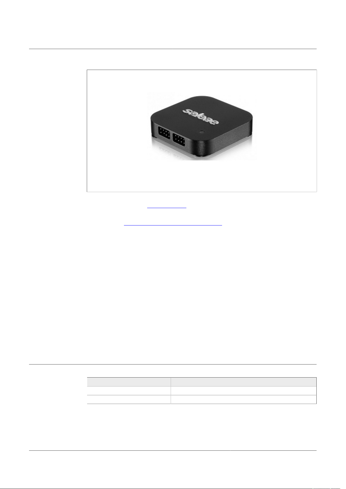
Note: The two TPL interface connectors are named J1 and J2 in the schematic diagram.
Figure 5. TPL bus connectors
5.1.1 Optional TPL bus loading
The TPL sniffer is designed to add minimal load to the TPL bus by default. Therefore, it
does not add any termination impedance and the differential load seen from the bus is
that of an input impedance of the MC33664 reflected on the high voltage side by the 1:1
ratio T1 isolation transformer.
In case an interface other than the default one is desired, some settings are possible on
the PCB:
•The two jumpers JP1 and JP2 located on the bottom side, should be closed (with a
drop of solder) in case a standard 150 Ω termination is desired.
•Additional component footprints are available on the top side of the PCB to
accommodate different loads on the TPL bus interface. These are R13 (default DNP)
and R14 and R15 (default 0 Ω).
Note: If the board must be modified and then powered without housing, proceed with
caution.
5.2 Power and data connections
The side of the case opposite the TPL connectors has all the other available connectors
of the TPL sniffer.
•The GND banana plug: used to connect, if necessary, the GND of the TPL sniffer to
another potential. It is labeled J5 in the schematics.
In some cases of use, the whole system including, for example, the TPL sniffer, the
power supply, the logic analyzer and the associated PC, could be an electrically
floating block. This connector allows, if desired, the ground potential of the system (for
example, the TPL sniffer and anything else that has its ground connected to the TPL
sniffer ground) to be set to any other convenient potential, that is, the protective earth
or the vehicle chassis ground (KL31).
•The data-out 8-pin connector: buffered SPI signals to be routed to the logic analyzer. It
is labeled J3 in the schematics. See Section 5.2.1 "Connecting to the logic analyzer" for
more details.
•The power-on LED indicator
UM11650 All information provided in this document is subject to legal disclaimers. © NXP B.V. 2021. All rights reserved.
User manual Rev. 1 — 4 August 2021
7 / 14

NXP Semiconductors UM11650
KIT-TPLSNIFEVB tool
•The USB Micro-B connector: to connect to a 5.0 V source. It is labeled J4 in the
schematics.
Figure 6. Power and data connectors
5.2.1 Connecting to the logic analyzer
The data output connector (J3) is an 8-pin 4x2 male connector used as an interface to
the logic analyzer, to transfer TPL messages converted to SPI format.
The signals are all unidirectional and their direction is from the TPL sniffer (output) to the
logic analyzer (input).
The TPL sniffer is designed such that the cable connection to the logic analyzer can
be relatively long, with a maximum length of 2 m, without loss of signal integrity and
therefore maintaining the logic and timing information.
This statement is only true if the following two rules are both satisfied:
•The cable used for the connection must have a characteristic impedance of 100 Ω. This
is the impedance normally found on standard IDC ribbon cables.
•The logic analyzer side of the cable should only be loaded with high impedance
terminations such as a High-Z input from an oscilloscope, for example, 15 pF || 1 MΩ,
or 5 pF || 10 MΩ (better), or digital inputs from a logic analyzer (for example, 10 pF || 2
MΩ).
Failure to follow these rules does not guarantee proper operation of the TPL sniffer,
unless the cable length is considerably short (< 15 cm) so that reflections in the cable can
be neglected.
For signal integrity and EMI reduction, the data lines are interleaved with the ground
potential with the pinout described in Table 1.
The TPL sniffer data output lines and the TPL inputs are internally protected by ESD
suppression devices. Nevertheless, standard electrostatic precautions should be taken
when handling and using the TPL sniffer.
The pin assignment for the data output connector is described in the following table:
Pin Signal Description
1 INTB SPI interrupt signal
2 GND Ground
3 RXCLK SPI bus clock
4 GND Ground
5 RXDATA SPI bus data
Table 1. ANALYZER connector (J3) pin assignment
UM11650 All information provided in this document is subject to legal disclaimers. © NXP B.V. 2021. All rights reserved.
User manual Rev. 1 — 4 August 2021
8 / 14

NXP Semiconductors UM11650
KIT-TPLSNIFEVB tool
Pin Signal Description
6 GND Ground
7 RXCSB SPI chip select
8 GND Ground
Table 1. ANALYZER connector (J3) pin assignment...continued
Figure 7. ANALYZER connector pinout
The supplied 8-pin connection cable should be plugged into the ANALYZER connector
with the blue wires on top (NXP logo side) and the black wires on the bottom.
5.2.1.1 Interfacing with the Saleae Logic Analyzer
The supplied 8-pin connectors cable is fitting the Saleae Logic 8 and Logic Pro 8/16
analyzer series input connectors. To connect to the Saleae Logic Analyzer, the cable
should be plugged with the blue wires on top (Saleae logo side) and the black wires on
the bottom.
UM11650 All information provided in this document is subject to legal disclaimers. © NXP B.V. 2021. All rights reserved.
User manual Rev. 1 — 4 August 2021
9 / 14

NXP Semiconductors UM11650
KIT-TPLSNIFEVB tool
Figure 8. Saleae Logic Analyzer
Saleae provides a software interface with its product to help decode the acquired signals.
To learn more, visit the Saleae website.
As a plug-in to the Saleae software interface, a DLL has been developed to decode TPL
frames. Go to http://www.nxp.com/KIT-TPLSNIFEVB for more details.
5.2.2 Powering the TPL sniffer
The TPL sniffer can be powered through the USB Micro-B connector (J4, labeled PWR)
by a 5.0 V source with 50 mA (average) and 150 mA (peak), typically a USB power bank
or a USB cable connected to a computer.
5.2.2.1 Power bank keep-alive function
The purpose of the keep-alive feature is to avoid the activation of the automatic shutdown
feature found on most consumer USB power banks. Such a shutdown would likely
occur due to the limited power consumption of the TPL sniffer circuit alone, in the 10
mA to 20 mA range. Therefore, the sniffer activates an additional 150 mA of internal
power consumption with a period of 5.8 seconds and a duty cycle of 20 % (all figures are
approximate). This simulates a load large enough to keep most power banks energized.
If the power-on LED indicator goes out shortly after the TPL sniffer is first powered up
with a power bank, consider trying another power bank model.
6 Hardware specifications
Description Value
Power supply voltage 5.0 V (± 10 %)
Power consumption < 50 mA (averaged over 20 seconds)
Table 2. Electrical characteristics
UM11650 All information provided in this document is subject to legal disclaimers. © NXP B.V. 2021. All rights reserved.
User manual Rev. 1 — 4 August 2021
10 / 14

NXP Semiconductors UM11650
KIT-TPLSNIFEVB tool
Description Value
Operating temperature 0 °C to 40 °C
Storage temperature -40 °C to 70 °C
Humidity 5 % to 95 % relative humidity, non-condensing
Table 3. Environmental characteristics
Description Value
Enclosure dimensions 72 mm W x 35 mm H x 103 mm D
TPL connectors (on TPL sniffer) MOLEX - Micro-Fit3.0 - 2-pin header. Reference No. 43650-0213
TPL connectors (on TPL cable) MOLEX - Micro-Fit3.0 - 2-pin receptacle. Reference No. 43645-0200
MOLEX - Micro-Fit3.0 - crimp pin. Reference No. 43030-0001
Power connector USB Micro-B receptacle
Data connector (on TPL sniffer) AMPHENOL - 4x2 header 2.54 mm. Reference No. 75867-132LF
GND connector HIRSHMANN - 2 mm Test socket. Reference No. 930224100
Table 4. Mechanical characteristics
7 References
[1] KIT-TPLSNIFEVB — detailed information on this board, including documentation, downloads, and software and tools
http://www.nxp.com/KIT-TPLSNIFEVB
[2] MC33664 — product information on MC33664, Isolated Network High-Speed Transceiver
http://www.nxp.com/MC33664
UM11650 All information provided in this document is subject to legal disclaimers. © NXP B.V. 2021. All rights reserved.
User manual Rev. 1 — 4 August 2021
11 / 14

NXP Semiconductors UM11650
KIT-TPLSNIFEVB tool
8 Legal information
8.1 Definitions
Draft — A draft status on a document indicates that the content is still
under internal review and subject to formal approval, which may result
in modifications or additions. NXP Semiconductors does not give any
representations or warranties as to the accuracy or completeness of
information included in a draft version of a document and shall have no
liability for the consequences of use of such information.
8.2 Disclaimers
Limited warranty and liability — Information in this document is believed
to be accurate and reliable. However, NXP Semiconductors does not
give any representations or warranties, expressed or implied, as to the
accuracy or completeness of such information and shall have no liability
for the consequences of use of such information. NXP Semiconductors
takes no responsibility for the content in this document if provided by an
information source outside of NXP Semiconductors. In no event shall NXP
Semiconductors be liable for any indirect, incidental, punitive, special or
consequential damages (including - without limitation - lost profits, lost
savings, business interruption, costs related to the removal or replacement
of any products or rework charges) whether or not such damages are based
on tort (including negligence), warranty, breach of contract or any other
legal theory. Notwithstanding any damages that customer might incur for
any reason whatsoever, NXP Semiconductors’ aggregate and cumulative
liability towards customer for the products described herein shall be limited
in accordance with the Terms and conditions of commercial sale of NXP
Semiconductors.
Right to make changes — NXP Semiconductors reserves the right to
make changes to information published in this document, including without
limitation specifications and product descriptions, at any time and without
notice. This document supersedes and replaces all information supplied prior
to the publication hereof.
Suitability for use — NXP Semiconductors products are not designed,
authorized or warranted to be suitable for use in life support, life-critical or
safety-critical systems or equipment, nor in applications where failure or
malfunction of an NXP Semiconductors product can reasonably be expected
to result in personal injury, death or severe property or environmental
damage. NXP Semiconductors and its suppliers accept no liability for
inclusion and/or use of NXP Semiconductors products in such equipment or
applications and therefore such inclusion and/or use is at the customer’s own
risk.
Applications — Applications that are described herein for any of these
products are for illustrative purposes only. NXP Semiconductors makes
no representation or warranty that such applications will be suitable
for the specified use without further testing or modification. Customers
are responsible for the design and operation of their applications and
products using NXP Semiconductors products, and NXP Semiconductors
accepts no liability for any assistance with applications or customer product
design. It is customer’s sole responsibility to determine whether the NXP
Semiconductors product is suitable and fit for the customer’s applications
and products planned, as well as for the planned application and use of
customer’s third party customer(s). Customers should provide appropriate
design and operating safeguards to minimize the risks associated with
their applications and products. NXP Semiconductors does not accept any
liability related to any default, damage, costs or problem which is based
on any weakness or default in the customer’s applications or products, or
the application or use by customer’s third party customer(s). Customer is
responsible for doing all necessary testing for the customer’s applications
and products using NXP Semiconductors products in order to avoid a
default of the applications and the products or of the application or use by
customer’s third party customer(s). NXP does not accept any liability in this
respect.
Terms and conditions of commercial sale — NXP Semiconductors
products are sold subject to the general terms and conditions of commercial
sale, as published at http://www.nxp.com/profile/terms, unless otherwise
agreed in a valid written individual agreement. In case an individual
agreement is concluded only the terms and conditions of the respective
agreement shall apply. NXP Semiconductors hereby expressly objects to
applying the customer’s general terms and conditions with regard to the
purchase of NXP Semiconductors products by customer.
Export control — This document as well as the item(s) described herein
may be subject to export control regulations. Export might require a prior
authorization from competent authorities.
Evaluation products — This product is provided on an “as is” and “with all
faults” basis for evaluation purposes only. NXP Semiconductors, its affiliates
and their suppliers expressly disclaim all warranties, whether express,
implied or statutory, including but not limited to the implied warranties of
non-infringement, merchantability and fitness for a particular purpose. The
entire risk as to the quality, or arising out of the use or performance, of this
product remains with customer. In no event shall NXP Semiconductors, its
affiliates or their suppliers be liable to customer for any special, indirect,
consequential, punitive or incidental damages (including without limitation
damages for loss of business, business interruption, loss of use, loss of
data or information, and the like) arising out the use of or inability to use
the product, whether or not based on tort (including negligence), strict
liability, breach of contract, breach of warranty or any other theory, even if
advised of the possibility of such damages. Notwithstanding any damages
that customer might incur for any reason whatsoever (including without
limitation, all damages referenced above and all direct or general damages),
the entire liability of NXP Semiconductors, its affiliates and their suppliers
and customer’s exclusive remedy for all of the foregoing shall be limited to
actual damages incurred by customer based on reasonable reliance up to
the greater of the amount actually paid by customer for the product or five
dollars (US$5.00). The foregoing limitations, exclusions and disclaimers shall
apply to the maximum extent permitted by applicable law, even if any remedy
fails of its essential purpose.
Translations — A non-English (translated) version of a document is for
reference only. The English version shall prevail in case of any discrepancy
between the translated and English versions.
Security — Customer understands that all NXP products may be subject
to unidentified or documented vulnerabilities. Customer is responsible
for the design and operation of its applications and products throughout
their lifecycles to reduce the effect of these vulnerabilities on customer’s
applications and products. Customer’s responsibility also extends to other
open and/or proprietary technologies supported by NXP products for use
in customer’s applications. NXP accepts no liability for any vulnerability.
Customer should regularly check security updates from NXP and follow up
appropriately. Customer shall select products with security features that best
meet rules, regulations, and standards of the intended application and make
the ultimate design decisions regarding its products and is solely responsible
for compliance with all legal, regulatory, and security related requirements
concerning its products, regardless of any information or support that may
be provided by NXP. NXP has a Product Security Incident Response Team
(PSIRT) (reachable at PSIR[email protected]) that manages the investigation,
reporting, and solution release to security vulnerabilities of NXP products.
8.3 Trademarks
Notice: All referenced brands, product names, service names and
trademarks are the property of their respective owners.
NXP — wordmark and logo are trademarks of NXP B.V.
UM11650 All information provided in this document is subject to legal disclaimers. © NXP B.V. 2021. All rights reserved.
User manual Rev. 1 — 4 August 2021
12 / 14

NXP Semiconductors UM11650
KIT-TPLSNIFEVB tool
Tables
Tab. 1. ANALYZER connector (J3) pin assignment .......8
Tab. 2. Electrical characteristics ..................................10
Tab. 3. Environmental characteristics ..........................11
Tab. 4. Mechanical characteristics .............................. 11
Figures
Fig. 1. KIT-TPLSNIFEVB ..............................................3
Fig. 2. TPL sniffer toolchain ......................................... 4
Fig. 3. Kit contents ....................................................... 5
Fig. 4. TPL sniffer block diagram ................................. 6
Fig. 5. TPL bus connectors .......................................... 7
Fig. 6. Power and data connectors .............................. 8
Fig. 7. ANALYZER connector pinout ............................ 9
Fig. 8. Saleae Logic Analyzer .................................... 10
UM11650 All information provided in this document is subject to legal disclaimers. © NXP B.V. 2021. All rights reserved.
User manual Rev. 1 — 4 August 2021
13 / 14

NXP Semiconductors UM11650
KIT-TPLSNIFEVB tool
Contents
1 Introduction ......................................................... 3
2 Finding kit resources and information on
the NXP web site ................................................ 4
3 Getting ready .......................................................4
3.1 Kit contents ........................................................4
3.2 Additional hardware and software ..................... 5
4 Getting to know the hardware ........................... 5
4.1 KIT-TPLSNIFEVB features ................................ 5
4.2 Block diagram ....................................................6
4.3 Schematics ........................................................ 6
5 Configuring the hardware .................................. 6
5.1 Connecting to the TPL bus ................................6
5.1.1 Optional TPL bus loading ..................................7
5.2 Power and data connections ............................. 7
5.2.1 Connecting to the logic analyzer ....................... 8
5.2.1.1 Interfacing with the Saleae Logic Analyzer ........ 9
5.2.2 Powering the TPL sniffer ................................. 10
5.2.2.1 Power bank keep-alive function .......................10
6 Hardware specifications ...................................10
7 References ......................................................... 11
8 Legal information .............................................. 12
Please be aware that important notices concerning this document and the product(s)
described herein, have been included in section 'Legal information'.
© NXP B.V. 2021. All rights reserved.
For more information, please visit: http://www.nxp.com
For sales office addresses, please send an email to: [email protected]
Date of release: 4 August 2021
Document identifier: UM11650
Table of contents