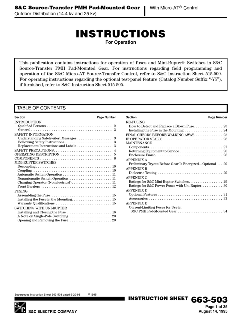
NXP Semiconductors PN5331B3HN User manual
Other NXP Semiconductors Controllers manuals
NXP Semiconductors
NXP Semiconductors PT2001 Operating instructions
NXP Semiconductors
NXP Semiconductors PN7150 User manual
NXP Semiconductors
NXP Semiconductors MC9S12ZVH64 User manual
NXP Semiconductors
NXP Semiconductors PN7150 Guide
NXP Semiconductors
NXP Semiconductors MC9328MX1 Manual
NXP Semiconductors
NXP Semiconductors PD3DB1548 PD3.0 type-C User manual
NXP Semiconductors
NXP Semiconductors MPC560xP Guide
NXP Semiconductors
NXP Semiconductors PXN2020 User manual
NXP Semiconductors
NXP Semiconductors 56F803 User manual
NXP Semiconductors
NXP Semiconductors 56800E User manual
NXP Semiconductors
NXP Semiconductors BLDC User manual
NXP Semiconductors
NXP Semiconductors TWR-K60N512 User manual
NXP Semiconductors
NXP Semiconductors PN7150 User manual
NXP Semiconductors
NXP Semiconductors PN7150X User manual
NXP Semiconductors
NXP Semiconductors OM5579 User manual
NXP Semiconductors
NXP Semiconductors DSP56800E User manual
NXP Semiconductors
NXP Semiconductors TWR-VF65GS10-PRO User manual
NXP Semiconductors
NXP Semiconductors 56F8300 Series User manual
NXP Semiconductors
NXP Semiconductors LPC1768 User manual
NXP Semiconductors
NXP Semiconductors K22F series User manual
Popular Controllers manuals by other brands
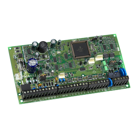
Digiplex
Digiplex DGP-848 Programming guide
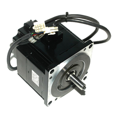
YASKAWA
YASKAWA SGM series user manual

Sinope
Sinope Calypso RM3500ZB installation guide
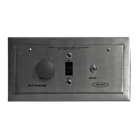
Isimet
Isimet DLA Series Style 2 Installation, Operations, Start-up and Maintenance Instructions
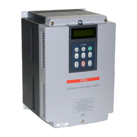
LSIS
LSIS sv-ip5a user manual
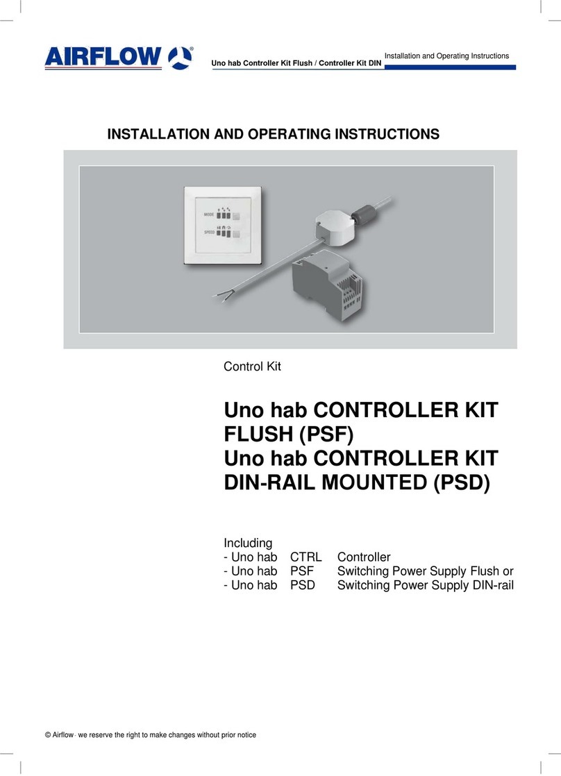
Airflow
Airflow Uno hab Installation and operating instructions


