NXP Semiconductors RDGD3162CSL3PEVM User manual

UM11996
RDGD3162CSL3PEVM three-phase inverter reference design
Rev. 1 — 22 November 2023 User manual
Document information
Information Content
Keywords GD3162, gate, driver, power, inverter, automotive
Abstract The RDGD3162CSL3PEVM three-phase inverter is a functional hardware power inverter
reference design, which can be used as a foundation to develop a complete ASIL D compliant
high voltage, high-power traction motor inverter for electric vehicles.

NXP Semiconductors UM11996
RDGD3162CSL3PEVM three-phase inverter reference design
1 Important notice
IMPORTANT NOTICE
For engineering development or evaluation purposes only
NXP provides the product under the following conditions:
This evaluation kit or reference design is for use of ENGINEERING DEVELOPMENT OR
EVALUATION PURPOSES ONLY.
It is provided as a sample IC pre-soldered to a printed circuit board to make it easier to access
inputs, outputs, and supply terminals. This evaluation kit or reference design may be used with any
development system or other source of I/O signals by connecting it to the host MCU or computer
board via off-the-shelf cables. Final device in an application will be heavily dependent on proper
printed circuit board layout and heat sinking design as well as attention to supply filtering, transient
suppression, and I/O signal quality.
The product provided may not be complete in terms of required design, marketing, and or
manufacturing related protective considerations, including product safety measures typically found
in the end device incorporating the product. Due to the open construction of the product, it is the
responsibility of the user to take all appropriate precautions for electric discharge. To minimize risks
associated with the customers’ applications, adequate design and operating safeguards must be
provided by the customer to minimize inherent or procedural hazards. For any safety concerns, contact
NXP sales and technical support services.
2 RDGD3162CSL3PEVM
Figure 1. RDGD3162CSL3PEVM
UM11996 All information provided in this document is subject to legal disclaimers. © 2023 NXP B.V. All rights reserved.
User manual Rev. 1 — 22 November 2023
2 / 35

NXP Semiconductors UM11996
RDGD3162CSL3PEVM three-phase inverter reference design
3 Introduction
This document is the user guide for the RDGD3162CSL3PEVM reference design. This document is intended for
the engineers involved in the evaluation, design, implementation, and validation of the GD3162 single-channel
gate driver for insulated gate bipolar transistor (IGBT)/SiC metal-oxide-semiconductor field-effect transistor
(MOSFET).
The scope of this document is to provide the user with information to evaluate the GD3162 single channel
gate driver for IGBT/SiC. This document covers connecting the hardware, installing the software and tools,
configuring the environment and using the kit.
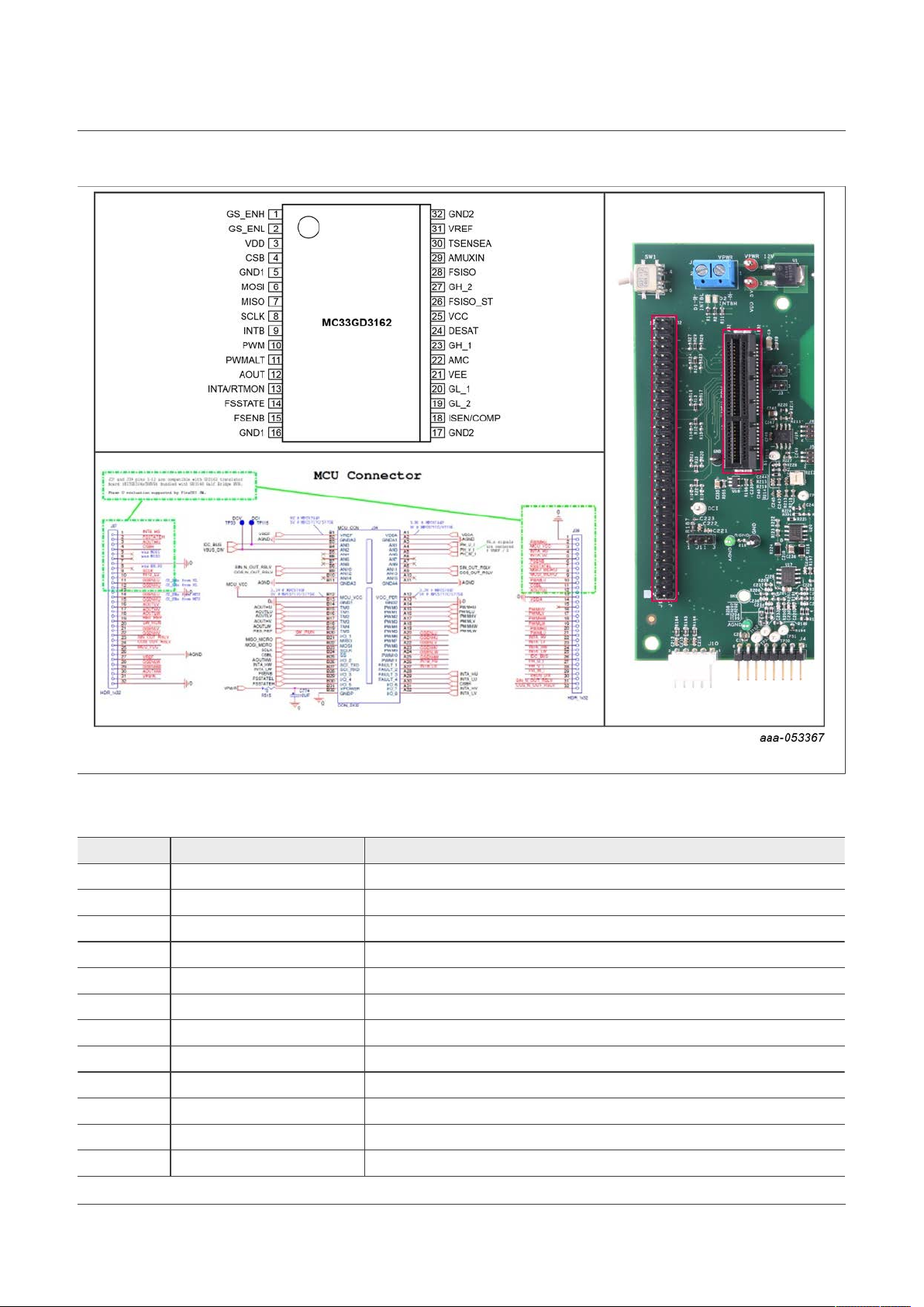
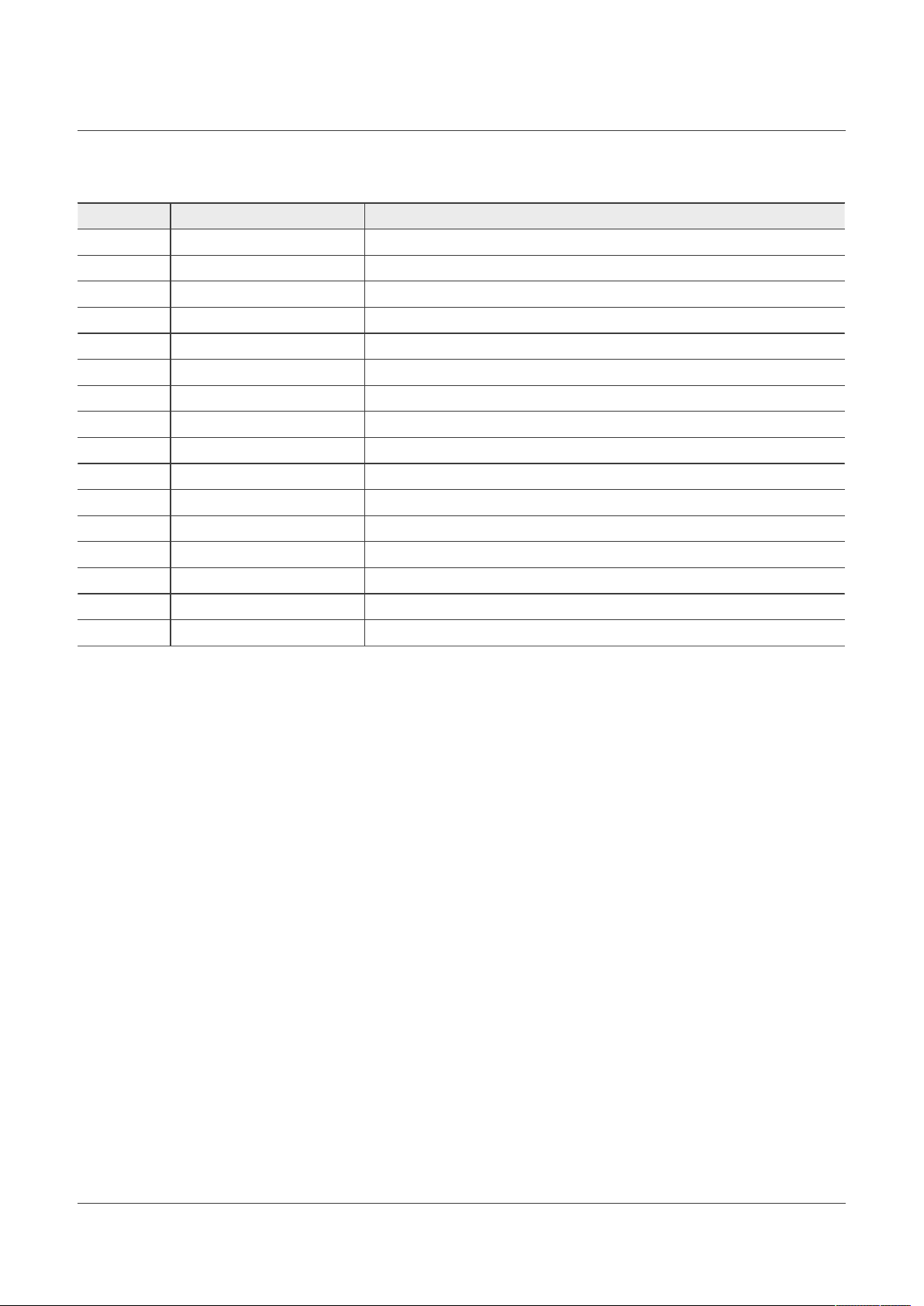
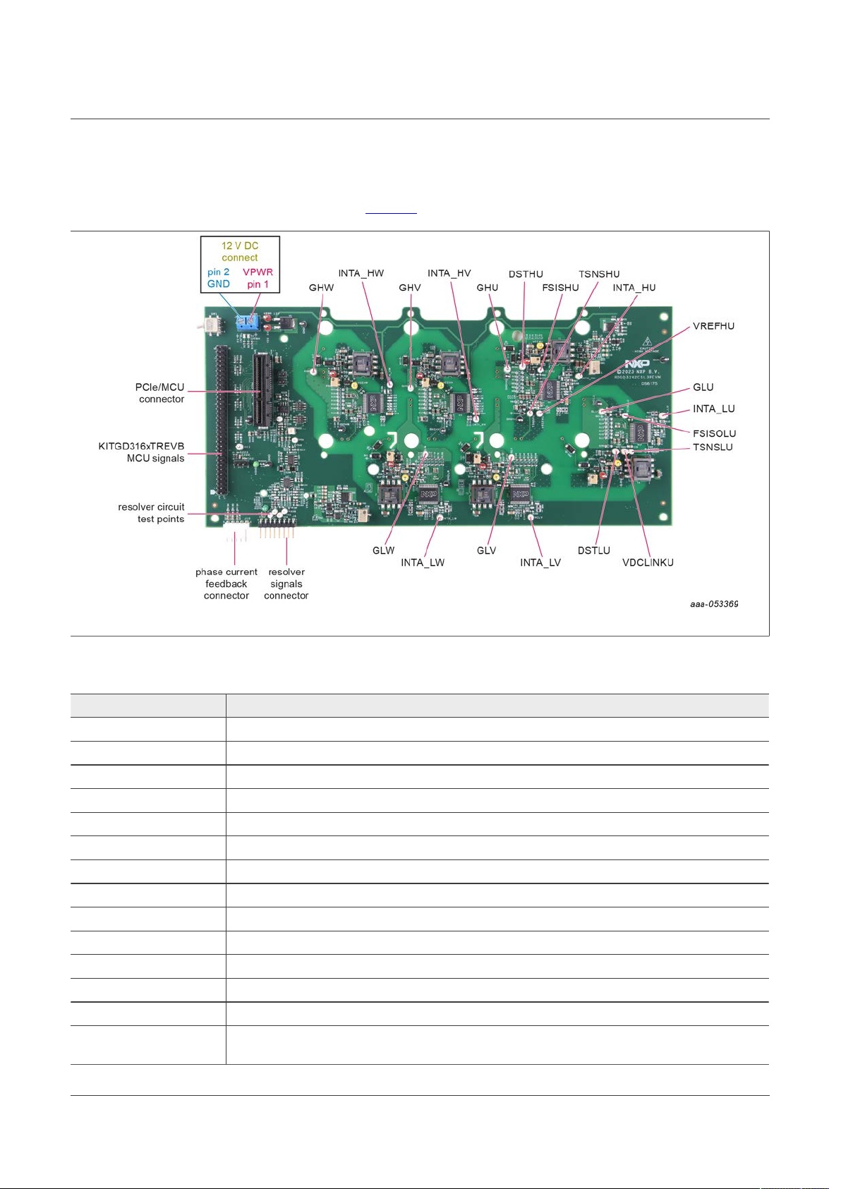
The RDGD3162CSL3PEVM is a fully functional three-phase inverter evaluation board populated with six
GD3162 gate drivers with fault management and supporting circuitry. This board supports serial peripheral
interface (SPI) daisy chain communication for programming and communication with three high-side gate
drivers and three low-side gate drivers independently, or all six gate drivers at the same time.
This board has low-voltage isolation and high-voltage isolation with gate drive integrated galvanic signal
isolation. Other supporting features on the board include desaturation short-circuit detection, IGBT/SiC
temperature sensing, onboard isolated flyback supplies, DC link bus voltage monitoring, phase current
sensing, DC link bus current sense, and motor resolver excitation/processing. See GD3162 data sheet https://
www.nxp.com/GD3162#documentation for more gate drive features. The data sheet requires a secure access
rights request to download the document.
4 Finding kit resources and information on the NXP website
NXP Semiconductors provides online resources for this reference design and its supported devices on http://
www.nxp.com.
The information page for the RDGD3162CSL3PEVM reference design is at http://www.nxp.com/
RDGD3162CSL3PEVM. The information page provides overview information, documentation, software
and tools, parametrics, ordering information and a Getting Started tab. The Getting Started tab provides
quick reference information applicable to using the RDGD3162CSL3PEVM reference design, including the
downloadable assets referenced in this document.
4.1 Collaborate in the NXP community
The NXP community is for sharing ideas and tips, ask and answer technical questions, and receive input on just
about any embedded design topic.
The NXP community is at http://community.nxp.com.
5 Getting ready
Working with the RDGD3162CSL3PEVM requires kit contents and a Windows PC workstation with FlexGUI
software installed.
5.1 Kit contents
•Assembled and tested RDGD3162CSL3PEVM (three-phase inverter populated with 5.0 V compatible gate
driver devices) board in an antistatic bag
•KITGD316xTREVB 3.3 V to 5.0 V translator with FRDM-KL25Z MCU board with micro‑USB cable
•Quick start guide
UM11996 All information provided in this document is subject to legal disclaimers. © 2023 NXP B.V. All rights reserved.
User manual Rev. 1 — 22 November 2023
3 / 35

NXP Semiconductors UM11996
RDGD3162CSL3PEVM three-phase inverter reference design
5.2 Additional hardware
In addition to the kit contents, the following hardware is beneficial when working with this reference board.
•Microcontroller for SPI communication
•Compatible Bosch compact silicon carbide line (CSL) B-sample SiC MOSFET module
•DC link capacitor compatible with SiC MOSFET module
•HV power supply with protection shield and hearing protection
•Current sensors for monitoring each phase current
•12 V, 1.0 A DC power supply
•4-channel oscilloscope with appropriate isolated probes
5.3 Windows PC workstation
This reference design requires a Windows PC workstation. Meeting these minimum specifications produces
great results when working with this evaluation board.
•USB-enabled computer with Windows 8 or Windows 10
5.4 Software
Installing software is necessary to work with this reference design. All listed software is available on the
information page at http://www.nxp.com/RDGD3162CSL3PEVM.
•FlexGUI software for using with KITGD316xTREVB MCU/translator board
•S32S Design Studio IDE for power architecture
•Automotive Math and Motor Control Library (AMMCLib)
•FreeMASTER 2.0 runtime debugging tool
•Motor control application tuning (MCAT)
•Example code, GD3162 device driver notes, and GD31xx device driver reference
6 Getting to know the hardware
6.1 RDGD3162CSL3PEVM features
•Capability to perform double pulse and short-circuit tests on phase U using KITGD316xTREVB and FlexGUI;
see phase U schematics and FlexGUI pulse tab (Figure 24 and Figure 25)
•Evaluation board designed for and populated with GD3162 gate drivers and protection circuitry
•Capability to connect to Bosch CSL B-sample SiC specific modules for full three-phase evaluation and
development (see Figure 9 for specific module pin placement)
•Daisy chain SPI communication × 3 - 2 channel (three high-side gate drivers and three low-side gate drivers)
or × 6 - 1 channel (all six gate drivers)
•Variable flyback VCC power supply with GND reference and variable negative VEE supply
•Easy access to power, ground, and signal test points
•2 × 32 peripheral component interconnect express (PCIe) socket for interfacing MCU control
(MPC5775B/E‑EVB, MPC5777C-DEVB, or MPC57744P); see Figure 26 and Figure 27
•Optional connection for DC bus voltage and current monitoring
•Phase current feedback connections
•Resolver signal connector
UM11996 All information provided in this document is subject to legal disclaimers. © 2023 NXP B.V. All rights reserved.
User manual Rev. 1 — 22 November 2023
4 / 35

NXP Semiconductors UM11996
RDGD3162CSL3PEVM three-phase inverter reference design
6.2 Kit featured components
6.2.1 Voltage domains, GD3162 pinout, logic header, and IGBT pinout
Low-voltage domain is an externally supplied 12 V DC (VPWR) primary supply for nonisolated circuits, typically
supplied by a vehicle battery. A 5 V regulator supplies VDD to GD3162 gate drive devices. The low-voltage
domain includes the interface between the MCU and GD3162 control registers and logic control.
Low-side driver and high-side driver domains are isolated high-voltage driver control domains for SiC MOSFET
or IGBT single phase connections and control circuits. Pins on the bottom of the board are designed to connect
easily to a compatible three-phase SiC MOSFET or IGBT module.
Figure 2. RDGD3162CSL3PEVM three-phase inverter board voltage domains and interfaces
6.2.2 GD3162 pinout and MCU interface pinout
See GD3162 advanced IGBT/SiC gate driver data sheet for specific information about pinout, pin descriptions,
specifications, and operating modes. VPWR DC supply terminal is a low-voltage input connection for supplying
power to the low-voltage nonisolated die and related circuitry. Typically supplied by vehicle battery +12 V DC.
MCU connector is a 2 × 32-pin PCIe interface connector for use with either MPC5775B/E-EVB or MPC5744P or
MPC5777C 32-bit MCU board or any other MCU of preference. An MCU is needed for SPI communication and
control of advanced IGBT/SiC gate drive devices (GD3162).
KITGD316xTREVB included with the kit (MCU and translator) can be attached to this board at the bottom of the
dual row header pin interface. All gate drivers can be accessed via SPI control using FlexGUI software.
Note: Double pulse and short-circuit tests can be conducted on phase U only. See FlexGUI pulse tab Figure 24
and Figure 25.
UM11996 All information provided in this document is subject to legal disclaimers. © 2023 NXP B.V. All rights reserved.
User manual Rev. 1 — 22 November 2023
5 / 35

NXP Semiconductors UM11996
RDGD3162CSL3PEVM three-phase inverter reference design
Figure 3. Gate driver pinout and board interface connection PCIe 2 × 32
Pin Name Function
A1 VDDA voltage reference resolver circuit
A2 GNDA1 analog ground
A3 PH_U_I current feedback phase U
A4 PH_V_I current feedback phase V
A5 PH_W_I current feedback phase W
A6 n.c. not connected
A7 n.c. not connected
A8 SIN_OUT_RSLV sine resolver signal
A9 COS_OUT_RSLV cosine resolver signal
A10 n.c. not connected
A11 GNDA4 analog ground
A12 VCC_PER 5.0 V MCU not connected
Table 1. PCIe MCU connector pin definitions
UM11996 All information provided in this document is subject to legal disclaimers. © 2023 NXP B.V. All rights reserved.
User manual Rev. 1 — 22 November 2023
6 / 35

NXP Semiconductors UM11996
RDGD3162CSL3PEVM three-phase inverter reference design
Pin Name Function
A13 GND2 ground
A14 PWMHU pulse width modulation (PWM) high-side phase U
A15 PWMLU pulse width modulation low-side phase U
A16 PWMHV pulse width modulation high-side phase V
A17 PWMLV pulse width modulation low-side phase V
A18 PWMHW pulse width modulation high-side phase W
A19 PWMLW pulse width modulation low-side phase W
A20 GSENLU GD3162 gate strength enable low-side phase U
A21 GSENHU GD3162 gate strength enable high-side phase U
A22 GSENLV GD3162 gate strength enable low-side phase V
A23 GSENHV GD3162 gate strength enable high-side phase V
A24 GSENLW GD3162 gate strength enable low-side phase W
A25 GSENHW GD3162 gate strength enable high-side phase W
A26 INTB_HS GD3162 fault reporting for high-side gate drive devices
A27 INTB_LS GD3162 fault reporting for low-side gate drive devices
A28 INTA_HU GD3162 fault reporting and real-time monitoring high-side phase U
A29 INTA_LU GD3162 fault reporting and real-time monitoring low-side phase U
A30 CSBH chip select bar to high gate drive devices
A31 INTA_HV GD3162 fault reporting and real-time monitoring high-side phase V
A32 INTA_LV GD3162 fault reporting and real-time monitoring low-side phase V
B1 VREF voltage reference from MCU
B2 GNDA2 analog ground
B3 IDC_BUS optional DC bus current measurement from DC bus current filter
B4 VBUS_DIV optional DC bus voltage divider monitoring (not used by default)
B5 n.c. not connected
B6 n.c. not connected
B7 n.c. not connected
B8 SIN_N_OUT_RSLV sine resolver signal
B9 COS_N_OUT_RSLV cosine resolver signal
B10 n.c. not connected
B11 GNDA3 analog ground
B12 MCU_VCC MCU VCC regulator voltage
B13 GND1 ground
B14 AOUTHU GD3162 analog output signal high-side U phase
B15 AOUTLU GD3162 analog output signal low-side U phase
B16 AOUTLV GD3162 analog output signal low-side V phase
Table 1. PCIe MCU connector pin definitions...continued
UM11996 All information provided in this document is subject to legal disclaimers. © 2023 NXP B.V. All rights reserved.
User manual Rev. 1 — 22 November 2023
7 / 35

NXP Semiconductors UM11996
RDGD3162CSL3PEVM three-phase inverter reference design
Pin Name Function
B17 AOUTHV GD3162 analog output signal high-side V phase
B18 AOUTLW GD3162 analog output signal low-side W phase
B19 RES_REF resolver reference voltage
B20 SW_RUN signal from onboard switch demo mode
B21 MISO_MICRO SPI slave out signal
B22 MOSI_MICRO SPI slave in signal
B23 SCLK SPI clock
B24 CSBL chip select bar to low-side gate drivers
B25 AOUTHW GD3162 analog output signal high-side W phase
B26 INTA_HW GD3162 fault reporting and real-time monitoring high-side phase W
B27 INTA_LW GD3162 fault reporting and real-time monitoring low-side phase W
B28 FSENB fail-safe state enable bar
B29 FSSTATEL fail-safe state low-side
B30 FSSTATEH fail-safe state high-side
B31 VPWR VPWR/VSUP 12 V voltage supply (low-voltage domain)
B32 GNDP ground connection (low-voltage domain)
Table 1. PCIe MCU connector pin definitions...continued
UM11996 All information provided in this document is subject to legal disclaimers. © 2023 NXP B.V. All rights reserved.
User manual Rev. 1 — 22 November 2023
8 / 35

NXP Semiconductors UM11996
RDGD3162CSL3PEVM three-phase inverter reference design
6.2.3 Test points
All test points are clearly marked on the board. Figure 4 shows the location of various test points.
Figure 4. RDGD3162CSL3PEVM test points
Test point name Function
DSTHU DESAT high-side U phase VCE desaturation connected to DESAT pin circuitry
DSTLU DESAT low-side U phase VCE desaturation connected to DESAT pin circuitry
FSISHU FSISO connection high-side U phase
FSISLU FSISO connection low-side U phase
GHU gate high-side U phase, which is the charging pin of the IGBT gate
GHV gate high-side V phase, which is the charging pin of the IGBT gate
GHW gate high-side W phase, which is the charging pin of the IGBT gate
GLU gate low-side U phase, which is the charging pin of the IGBT gate
GLV gate low-side V phase, which is the charging pin of the IGBT gate
GLW gate low-side W phase, which is the charging pin of the IGBT gate
INTA – UVW HS and LS INTA interrupt/real-time reporting output signal test points from each gate driver
Resolver circuit test points for internal signals of the resolver circuit (see schematic for more information)
MCU signals signal headers for analyzing all MCU signals (see schematic for signals)
TSNSHU TSENSE high-side U phase connected to negative temperature coefficient (NTC) temperature
sense
Table 2. Test points
UM11996 All information provided in this document is subject to legal disclaimers. © 2023 NXP B.V. All rights reserved.
User manual Rev. 1 — 22 November 2023
9 / 35

NXP Semiconductors UM11996
RDGD3162CSL3PEVM three-phase inverter reference design
Test point name Function
TSNSLU TSENSE low-side U phase
VREFLU 5.0 V reference voltage test point low-side U phase
VREFHU 5.0 V reference voltage test point high-side U phase
VPWR VSUP/VPWR test point low-voltage domain
Table 2. Test points...continued
6.2.4 Indicators
The RDGD3162CSL3PEVM contains LEDs as visual indicators on the board.
Figure 5. RDGD3162CSL3PEVM indicator locations
Name Description
INTBL LED indicates that a GD3162 INTB fault interrupt has occurred on the low side
INTBH LED indicates that a GD3162 INTB fault interrupt has occurred on the high side
Table 3. RDGD3162CSL3PEVM indicator descriptions
UM11996 All information provided in this document is subject to legal disclaimers. © 2023 NXP B.V. All rights reserved.
User manual Rev. 1 — 22 November 2023
10 / 35

NXP Semiconductors UM11996
RDGD3162CSL3PEVM three-phase inverter reference design
6.2.5 Connectors and jumpers
Figure 6. RDGD3162CSL3PEVM connector and jumper locations
Name Description
J12 VPWR to VRSLV (12 V resolver excitation circuit)
jumper closed to VPWR supply to power resolver logic
J2 jumper 1-2 default master output slave input (MOSI) - normal mode three device daisy
chain three device high side, three device low side (× 3 - 2 channel)
jumper 2-3 MOSI - six device daisy chain all six gate drivers daisy chained together
(× 6 - 1 channel)
J3 jumper 1-2 default master input slave output (MISO) - normal mode three device daisy
chain three device high side, three device low side (× 3 - 2 channel)
jumper 2-3 MISO - six device daisy chain all six gate drivers daisy chained together
(× 6 - 1 channel)
J5 KITGD316xTREVB PWMH connection selection to high-side gate drive PWM inputs;
phase U, V, W; refer to schematic for details
J6 KITGD316xTREVB PWML connection selection to low-side gate drive PWM inputs;
phase U, V, W; refer to schematic for details
J11 DC bus current measurement connection header; refer to schematic for details
J10 phase current feedback
connector
current feedback connections from U, V, and W phases
J4 resolver signals connector resolver excitation signals; refer to schematic for details
J9 and J8 MCU signals two-row header of all MCU signals for debug and development; refer to schematic for
details
Table 4. RDGD3162CSL3PEVM connector and jumper descriptions
UM11996 All information provided in this document is subject to legal disclaimers. © 2023 NXP B.V. All rights reserved.
User manual Rev. 1 — 22 November 2023
11 / 35

NXP Semiconductors UM11996
RDGD3162CSL3PEVM three-phase inverter reference design
Name Description
J8 PCIe/MCU connector 2 × 32 PCIe connector for easy connection to MPC5777CDEVB or MPC5744P via PCIe
cable (S32SDEV-CON18)
J1 VPWR terminal connector used for external low-voltage power supply connection, typically 12 V VBAT
Table 4. RDGD3162CSL3PEVM connector and jumper descriptions...continued
6.2.6 Power supply test points
Figure 7. Power supply test point locations
Name Function
VCCHU high-side phase U VCC voltage test point
isolated positive voltage supply (9.3 V to 25 V)
adjust with R51 potentiometer
GNDHU isolated ground high-side phase U
VEEHU negative gate supply voltage high-side phase U
adjust with R32 potentiometer
VCCHV high-side phase V VCC voltage test point
isolated positive voltage supply (9.3 V to 25 V)
adjust with R51 potentiometer
GNDHV isolated ground high-side phase V
VEEHV negative gate supply voltage high-side phase V
adjust with R46 potentiometer
Table 5. Power supply test point descriptions
UM11996 All information provided in this document is subject to legal disclaimers. © 2023 NXP B.V. All rights reserved.
User manual Rev. 1 — 22 November 2023
12 / 35

NXP Semiconductors UM11996
RDGD3162CSL3PEVM three-phase inverter reference design
Name Function
VCCHW high-side phase W VCC voltage test point
isolated positive voltage supply (9.3 V to 25 V)
adjust with R51 potentiometer
GNDHW isolated ground high-side phase W
VEEHW negative gate supply voltage high-side phase W
adjust with R53 potentiometer
VCCLU low-side phase U VCC voltage test point
isolated positive voltage supply (9.3 V to 25 V)
adjust with R76 potentiometer
GNDLU isolated ground low-side phase U
VEELU negative gate supply voltage low-side phase U
adjust with R57 potentiometer
VCCLV low-side phase V VCC voltage test point
isolated positive voltage supply (9.3 V to 25 V)
adjust with R76 potentiometer
GNDLV isolated ground low-side phase V
VEELV negative gate supply voltage low-side phase V
adjust with R71 potentiometer
VCCLW low-side phase W VCC voltage test point
isolated positive voltage supply (9.3 V to 25 V)
adjust with R76 potentiometer
GNDLW isolated ground low-side phase W
VEELW negative gate supply voltage low-side phase W
adjust with R78 potentiometer
VPWR +12 V DC VPWR low voltage positive supply connection
VPWR GND VPWR low voltage supply ground connection (GND)
Table 5. Power supply test point descriptions...continued
6.2.7 Gate drive resistors (not populated)
•RGH_1 - gate high resistor in series with the GH_1 pin at the output of the GD3162 high-side driver and
IGBT/SiC gate that controls the strong turn on current for IGBT/SiC gate.
•RGH_2 - gate high resistor in series with the GH_2 pin at the output of the GD3162 high-side driver and
IGBT/SiC gate that controls the weak turn on current for IGBT/SiC gate.
•RGL_1 - gate low resistor in series with the GL_1 pin at the output of the GD3162 low-side driver and
IGBT/SiC gate that controls the strong turn off current for IGBT/SiC gate.
•RGL_2 - gate low resistor in series with the GL_2 pin at the output of the GD3162 low-side driver and
IGBT/SiC gate that controls the weak turn off current for IGBT/SiC gate.
•RAMC - series resistor between IGBT/SiC gate and active Miller clamp (AMC) input pin of the GD3162
high‑side/low-side driver for gate sensing and active Miller clamping.
UM11996 All information provided in this document is subject to legal disclaimers. © 2023 NXP B.V. All rights reserved.
User manual Rev. 1 — 22 November 2023
13 / 35

NXP Semiconductors UM11996
RDGD3162CSL3PEVM three-phase inverter reference design
Figure 8. Gate drive resistors for each phase high side and low side
6.2.8 Bosch CSL B-sample SiC module pin connections
Figure 9. SiC module pin placement
UM11996 All information provided in this document is subject to legal disclaimers. © 2023 NXP B.V. All rights reserved.
User manual Rev. 1 — 22 November 2023
14 / 35

NXP Semiconductors UM11996
RDGD3162CSL3PEVM three-phase inverter reference design
Figure 10. SiC module pin connections
Connection name Pin description
GHU gate high-side U phase
DHU drain connection high-side U phase
SHU source connection high-side U phase
PTCU1 positive temperature coefficient (PTC) temperature sensor connection U phase (high-side
TSENSEA)
PTCU2 PTC temperature sensor connection U phase (high-side isolated ground)
GLU gate low-side U phase
SLU source connection low-side U phase
DLU drain connection low-side U phase
PTCV1 PTC temperature sensor connection V phase (high-side TSENSEA)
PTCV2 PTC temperature sensor connection V phase (high-side isolated ground)
GHV gate high-side V phase
SHV source connection high-side V phase
DHV drain connection high-side V phase
GLV gate low-side V phase
DLV drain connection low-side V phase
SLV source connection low-side V phase
PTCW1 PTC temperature sensor connection W phase (high-side TSENSEA)
PTCW2 PTC temperature sensor connection W phase (high-side isolated ground)
GHW gate high-side W phase
Table 6. SiC module pin connections
UM11996 All information provided in this document is subject to legal disclaimers. © 2023 NXP B.V. All rights reserved.
User manual Rev. 1 — 22 November 2023
15 / 35

NXP Semiconductors UM11996
RDGD3162CSL3PEVM three-phase inverter reference design
Connection name Pin description
DHW drain connection high-side W phase
SHW source connection high-side W phase
GLW gate low-side W phase
DLW drain connection low-side W phase
SLW source connection low-side W phase
Table 6. SiC module pin connections...continued
6.3 Kinetis KL25Z Freedom board
The Freedom KL25Z is an ultra low-cost development platform for Kinetis L series MCU built on Arm
Cortex‑M0+ processor.
Figure 11. Freedom development platform
UM11996 All information provided in this document is subject to legal disclaimers. © 2023 NXP B.V. All rights reserved.
User manual Rev. 1 — 22 November 2023
16 / 35

NXP Semiconductors UM11996
RDGD3162CSL3PEVM three-phase inverter reference design
6.4 3.3 V to 5.0 V translator board
KITGD316xTREVB translator enables level shifting of signals from MCU 3.3 V to 5.0 V SPI communication.
Figure 12. Translator board
Jumper Position Function
1-2 selects 5.0 V for 5.0 V compatible gate driveVCCSEL (J3)
2-3 selects 3.3 V for 3.3 V compatible gate drive
1-2 selects PWM high-side control from KL25Z MCUPWMH_SEL (J4)
2-3 selects PWM high-side control from fiber optic receiver inputs
1-2 selects PWM low-side control from KL25Z MCUPWML_SEL (J5)
2-3 selects PWM low-side control from fiber optic receiver inputs
Table 7. Translator board jumper definitions
7 Installing and configuring software and tools
Software for RDGD3162CSL3PEVM is distributed with the FlexGUI tool (available on NXP.com). Necessary
firmware comes preinstalled on the FRDM-KL25Z with the kit.
Even if you intend to test with other software or PWM, it is recommended to install this software as a backup or
to help debugging.
UM11996 All information provided in this document is subject to legal disclaimers. © 2023 NXP B.V. All rights reserved.
User manual Rev. 1 — 22 November 2023
17 / 35

NXP Semiconductors UM11996
RDGD3162CSL3PEVM three-phase inverter reference design
7.1 Installing FlexGUI on your computer
The latest version of FlexGUI supports the GD3100, GD3160, and GD3162. It is designed to run on any
Windows 10 or Windows 8 based operating system. To install the software, do the following:
1. Go to www.nxp.com/FlexGUI and click Download.
2. When the FlexGUI software page appears, click Download and select the version associated with your PC
operating system.
3. The FlexGUI wizard creates a shortcut. An NXP FlexGUI icon appears on the desktop. Installing the device
drivers overwrites any previous FlexGUI installation and replaces it with a current version containing the
GD31xx drivers. However, configuration files (.spi) from the previous version remain intact.
7.2 Configuring the FRDM-KL25Z microcode
Figure 13. FRDM-KL25Z setup and interface
By default, the FRDM-KL25Z delivered with this kit is preprogrammed with the current and most up-to-date
firmware available for the kit.
A way to check quickly that the microcode is programmed and the board is functioning properly, is to plug the
KL25Z into the computer using a USB cable to the USBKL25Z port, open FlexGUI, and verify that the software
version at the bottom is 8.7 or later (see Figure 13).
If a loss of functionality following a board reset, reprogramming, or a corrupted data issue, the microcode is
rewritten per the following steps:
UM11996 All information provided in this document is subject to legal disclaimers. © 2023 NXP B.V. All rights reserved.
User manual Rev. 1 — 22 November 2023
18 / 35

NXP Semiconductors UM11996
RDGD3162CSL3PEVM three-phase inverter reference design
1. To clear the memory and place the board in bootloader mode, hold down the reset button while plugging a
USB cable into the OpenSDA USB port.
2. Verify that the board appears as a BOOTLOADER device and continue with step 3. If the board appears as
KL25Z, go to step 6.
3. Download the Firmware Apps.zip archive from the PEmicro OpenSDA webpage (http://www.pemicro.com/
opensda/). Validate your email address to access the files.
4. Find the most recent MDS-DEBUG-FRDM-KL25Z_Pemicro_v118.SDA and copy/drag-and-drop into the
BOOTLOADER device.
5. Reboot the board by unplugging and replugging the connection to the OpenSDA port. Verify now that the
device appears as a KL25Z device to continue.
6. Locate the most recent KL25Z firmware, which is distributed as part of the FlexGUI package.
a. FlexGUI download file is named in the form “flexgui-fw-KL25Z_usb_hid_gd31xxC_vx.x.x.bin”.
b. This .bin file is a product/family-specific configuration file for FRDM-KL25Z containing the pin definitions,
SPI/PWM generation code, and pin-mapping assignments necessary to interface with the translator
board as part of RDGD3162CSL3PEVM.
7. With the KL25Z still plugged through the OpenSDA port, copy/drag-and-drop the .bin file into the KL25Z
device memory. Once done, disconnect the USB and plug into the other USB port, labeled KL25Z.
a. The device does not appear as a distinct device to the computer while connected through the KL25Z
USB port, which is normal.
8. The FRDM-KL25Z board is now fully set up to work with RDGD3162CSL3PEVM and the FlexGUI.
a. There is no software stored or present on either the driver or translator boards, only on the
FRDM‑KL25Z MCU board.
All uploaded firmware is stored in nonvolatile memory until the reset button is hit on the FRDM-KL25Z. There
is no need to repeat this process upon every power up, and there is no loss of data associated with a single
unplug event.
7.3 Using the FlexGUI
The FlexGUI is available from http://www.nxp.com/FlexGUI as an evaluation tool demonstrating
GD31xx‑specific functionality, configuration, and fault reporting. FlexGUI also includes basic capacity for the
RDGD3162CSL3PEVM to control an IGBT or SiC module, enabling double pulse or short-circuit testing.
SPI messages can be realized graphically or in hexadecimal format. CSB is selectable to address one or both
GD31xx on the board via daisy chain. See Figure 14 to Figure 24 for FlexGUI for GD31xx internal register read
and write access.
Starting FlexGUI for GD31xx
•FlexGUI install program (NXP_GD31xx_GUI-0.x.x.msi)
•Download FlexGUI and run the install program on your PC.
•When you start the application, Figure 14 allows you to select the target application board, feature set
(standard or daisy chain), target MCU, and USB interface. Leave all settings as shown.
Once the kit is selected press Ok and “START” FlexGUI on the following GUI page. Micro-USB cable must be
attached from PC and KL25Z port on KL25Z board.
UM11996 All information provided in this document is subject to legal disclaimers. © 2023 NXP B.V. All rights reserved.
User manual Rev. 1 — 22 November 2023
19 / 35

NXP Semiconductors UM11996
RDGD3162CSL3PEVM three-phase inverter reference design
See Table 4 for required jumper configuration to enable [× 3 - 2 channel (default)] or (× 6 - 1 channel) SPI daisy chain
operation.
Figure 14. Kit selection
UM11996 All information provided in this document is subject to legal disclaimers. © 2023 NXP B.V. All rights reserved.
User manual Rev. 1 — 22 November 2023
20 / 35
Table of contents
Other NXP Semiconductors Inverter manuals
Popular Inverter manuals by other brands

Alpha ESS
Alpha ESS SMILE-T10-HV-INV Quick installation guide

Expert Power
Expert Power IVOCH2KW owner's manual

FRONIUS
FRONIUS FRONIUS IS 15 operating instructions

VOLTCRAFT
VOLTCRAFT CSI-150 operating instructions

Hitachi
Hitachi SJ300-EL Series Instruction manual supplement

Hitachi
Hitachi NES1-004SB Quick reference guide

Westerbeke
Westerbeke 7.6 kw EDT Operator's manual

Sherman hobby
Sherman hobby MMA 200 SPeeDY user manual

Olimpia splendid
Olimpia splendid Nexya S4 E Series Instructions for use and maintenance

SunSynk
SunSynk SYNK-8K-SG04LP3 Installer manual

Rheem
Rheem GEN-12S Warranty

Omega
Omega INTERLAGOS OM3500 PRO user guide