ON Semiconductor CAT24C01 User manual

©Semiconductor Components Industries, LLC, 2013
February, 2013 −Rev. 26
1Publication Order Number:
CAT24C01/D
CAT24C01, CAT24C02,
CAT24C04, CAT24C08,
CAT24C16
1-Kb, 2-Kb, 4-Kb, 8-Kb and
16-Kb I2C CMOS Serial
EEPROM
Description
The CAT24C01/02/04/08/16 are 1−Kb, 2−Kb, 4−Kb, 8−Kb and
16−Kb respectively CMOS Serial EEPROM devices organized
internally as 8/16/32/64 and 128 pages respectively of 16 bytes each.
All devices support both the Standard (100 kHz) as well as Fast
(400 kHz) I2C protocol.
Data is written by providing a starting address, then loading 1 to 16
contiguous bytes into a Page Write Buffer, and then writing all data to
non−volatile memory in one internal write cycle. Data is read by
providing a starting address and then shifting out data serially while
automatically incrementing the internal address count.
External address pins make it possible to address up to eight
CAT24C01 or CAT24C02, four CAT24C04, two CAT24C08 and one
CAT24C16 device on the same bus.
Features
•Supports Standard and Fast I2C Protocol
•1.7 V to 5.5 V Supply Voltage Range
•16−Byte Page Write Buffer
•Hardware Write Protection for Entire Memory
•Schmitt Triggers and Noise Suppression Filters on I2C Bus Inputs
(SCL and SDA)
•Low power CMOS Technology
•More than 1,000,000 Program/Erase Cycles
•100 Year Data Retention
•Industrial and Extended Temperature Range
•These Devices are Pb−Free, Halogen Free/BFR Free and are RoHS
Compliant
SDA
SCL
WP
VCC
VSS
1
2
3
4
8
7
6
5
CAT24C__
16 / 08 / 04 / 02 / 01
NC ////
NC NC
NC NC
NC
A0A0
A1A1A1
A2A2A2
A2
////
////
PIN CONFIGURATION
PDIP (L), SOIC (W), TSSOP (Y), MSOP (Z),
* The TDFN (VP2) package is not recommended for new designs.
TDFN, (VP2)*, UDFN−EP (HU4) (Top View)
See detailed ordering and shipping information in the package
dimensions section on page 19 of this data sheet.
ORDERING INFORMATION
http://onsemi.com
SOIC−8
W SUFFIX
CASE 751BD
TSOT−23
TD SUFFIX
CASE 419AE
PDIP−8
L SUFFIX
CASE 646AA
TSSOP−8
Y SUFFIX
CASE 948AL
MSOP−8
Z SUFFIX
CASE 846AD
TDFN−8*
VP2 SUFFIX
CASE 511AK
VCC
WP
SDA
VSS
SCL 1
2
3
5
4
TSOT−23 (TD), TSOP−5** (TS) (Top View)
PIN CONFIGURATIONS
UDFN8−EP
HU4 SUFFIX
CASE 517AZ
WLCSP−4***
C4A SUFFIX
CASE 567DC
WLCSP−5***
C5A SUFFIX
CASE 567DD
*** WLCSP are available for the CAT24C04,
CAT24C08 and CAT24C16 only.
TOP MARKING FOR WLCSP
X = Specific Device
X = Code
4 = 24C04
8 = 24C08
6 = 24C16
Y = Production Year (Last Digit)
M = Production Month (1−9, O, N, D)
WLCSP−4 WLCSP−5
WLCSP−4*** WLCSP−5***
(Top Views)
WP SCL
SDA
SCL SDA
Pin 1
A
12312
B
C
A
B
Pin 1
VCC VSS
VCC VSS
X X
Y M Y M
Pin 1
(Ball Down)
Pin 1
TSOP−5**
TS SUFFIX
CASE 483
** TSOP are available for the CAT24C02 only.

CAT24C01, CAT24C02, CAT24C04, CAT24C08, CAT24C16
http://onsemi.com
2
SCL
WP
CAT24Cxx
Figure 1. Functional Symbol
VSS
SDA
VCC
A2, A1, A0
Table 1. PIN FUNCTION
Pin Name†Function
A0, A1, A2 Device Address Input
SDA Serial Data Input/Output
SCL Serial Clock Input
WP Write Protect Input
VCC Power Supply
VSS Ground
NC No Connect
†The exposed pad for the TDFN/UDFN packages can be left floating
or connected to Ground.
Table 2. ABSOLUTE MAXIMUM RATINGS
Parameters Ratings Units
Storage Temperature −65 to +150 °C
Voltage on any pin with respect to Ground (Note 1) −0.5 to +6.5 V
Stresses exceeding Maximum Ratings may damage the device. Maximum Ratings are stress ratings only. Functional operation above the
Recommended Operating Conditions is not implied. Extended exposure to stresses above the Recommended Operating Conditions may affect
device reliability.
1. During input transitions, voltage undershoot on any pin should not exceed −1 V for more than 20 ns. Voltage overshoot on pins A0, A1, A2
and WP should not exceed VCC + 1 V for more than 20 ns, while voltage on the I2C bus pins, SCL and SDA, should not exceed the absolute
maximum ratings, irrespective of VCC.
Table 3. RELIABILITY CHARACTERISTICS (Note 2)
Symbol Parameter Min Units
NEND (Note 3) Endurance 1,000,000 Program / Erase Cycles
TDR Data Retention 100 Years
2. These parameters are tested initially and after a design or process change that affects the parameter according to appropriate AEC−Q100
and JEDEC test methods.
3. Page Mode, VCC = 5 V, 25°C.
Table 4. D.C. OPERATING CHARACTERISTICS
(VCC = 1.8 V to 5.5 V, TA= −40°C to +125°C and VCC = 1.7 V to 5.5 V, TA= −40°C to +85°C, unless otherwise specified.)
Symbol Parameter Test Conditions Min Max Units
ICCR Read Current Read, fSCL = 400 kHz 1 mA
ICCW Write Current Write, fSCL = 400 kHz 2 mA
ISB Standby Current All I/O Pins at GND or VCC TA= −40°C to +85°C
VCC ≤3.3 V
1mA
TA= −40°C to +85°C
VCC > 3.3 V
3
TA= −40°C to +125°C 5
ILI/O Pin Leakage Pin at GND or VCC 2mA
VIL Input Low Voltage −0.5 0.3 x VCC V
VIH Input High Voltage A0, A1, A2and WP 0.7 x VCC VCC + 0.5 V
SCL and SDA 0.7 x VCC 5.5
VOL Output Low
Voltage
VCC > 2.5 V, IOL = 3 mA 0.4
VCC < 2.5 V, IOL = 1 mA 0.2

CAT24C01, CAT24C02, CAT24C04, CAT24C08, CAT24C16
http://onsemi.com
3
Table 5. PIN IMPEDANCE CHARACTERISTICS
(VCC = 1.8 V to 5.5 V, TA= −40°C to +125°C and VCC = 1.7 V to 5.5 V, TA= −40°C to +85°C, unless otherwise specified.)
Symbol Parameter Conditions Max Units
CIN (Note 4) SDA Pin Capacitance VIN = 0 V, f = 1.0 MHz, VCC = 5.0 V 8 pF
Other Pins 6 pF
IWP (Note 5) WP Input Current VIN < VIH, VCC = 5.5 V 130 mA
VIN < VIH, VCC = 3.3 V 120
VIN < VIH, VCC = 1.7 V 80
VIN > VIH 2
IA(Note 5) Address Input Current
(A0, A1, A2)
Product Rev H: CAT24C02
Product Rev K: CAT24C04,
CAT24C08, CAT24C16
VIN < VIH, VCC = 5.5 V 50 mA
VIN < VIH, VCC = 3.3 V 35
VIN < VIH, VCC = 1.7 V 25
VIN > VIH 2
4. These parameters are tested initially and after a design or process change that affects the parameter according to appropriate AEC−Q100
and JEDEC test methods.
5. When not driven, the WP, A0, A1 and A2 pins are pulled down to GND internally. For improved noise immunity, the internal pull−down is
relatively strong; therefore the external driver must be able to supply the pull−down current when attempting to drive the input HIGH. To
conserve power, as the input level exceeds the trip point of the CMOS input buffer (~ 0.5 x VCC), the strong pull−down reverts to a weak
current source.
Table 6. A.C. CHARACTERISTICS
(Note 6) (VCC = 1.8 V to 5.5 V, TA= −40°C to +125°C and VCC = 1.7 V to 5.5 V, TA= −40°C to +85°C, unless otherwise specified.)
Symbol Parameter
Standard Fast
Units
Min Max Min Max
FSCL Clock Frequency 100 400 kHz
tHD:STA START Condition Hold Time 4 0.6 ms
tLOW Low Period of SCL Clock 4.7 1.3 ms
tHIGH High Period of SCL Clock 4 0.6 ms
tSU:STA START Condition Setup Time 4.7 0.6 ms
tHD:DAT Data In Hold Time 0 0 ms
tSU:DAT Data In Setup Time 250 100 ns
tRSDA and SCL Rise Time 1000 300 ns
tF(Note 6) SDA and SCL Fall Time 300 300 ns
tSU:STO STOP Condition Setup Time 4 0.6 ms
tBUF Bus Free Time Between STOP and START 4.7 1.3 ms
tAA SCL Low to Data Out Valid 3.5 0.9 ms
tDH Data Out Hold Time 100 100 ns
Ti(Note 6) Noise Pulse Filtered at SCL and SDA Inputs 100 100 ns
tSU:WP WP Setup Time 0 0 ms
tHD:WP WP Hold Time 2.5 2.5 ms
tWR Write Cycle Time 5 5 ms
tPU (Notes 7, 8) Power−up to Ready Mode 1 1 ms
6. Test conditions according to “AC Test Conditions” table.
7. Tested initially and after a design or process change that affects this parameter.
8. tPU is the delay between the time VCC is stable and the device is ready to accept commands.

CAT24C01, CAT24C02, CAT24C04, CAT24C08, CAT24C16
http://onsemi.com
4
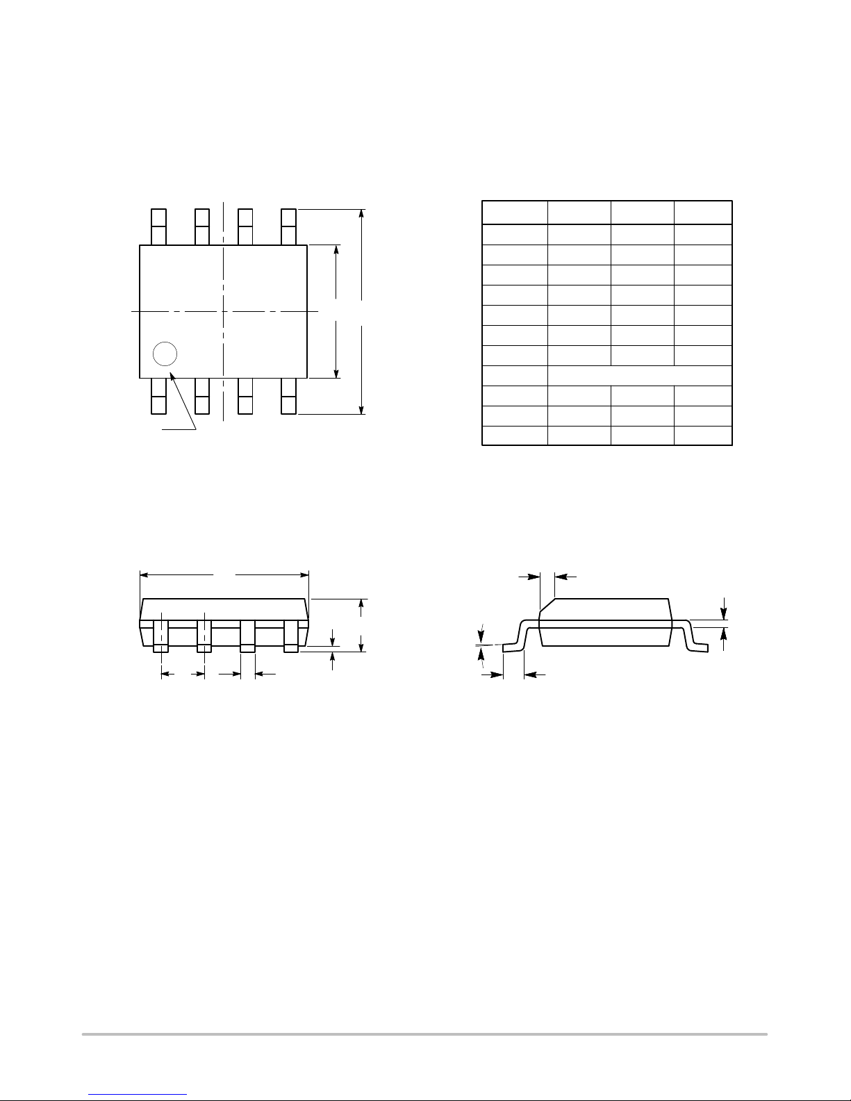
Table 7. A.C. TEST CONDITIONS
Input Drive Levels 0.2 x VCC to 0.8 x VCC
Input Rise and Fall Time v50 ns
Input Reference Levels 0.3 x VCC, 0.7 x VCC
Output Reference Level 0.5 x VCC
Output Test Load Current Source IOL = 3 mA (VCC w2.5 V); IOL = 1 mA (VCC < 2.5 V); CL= 100 pF
Power−On Reset (POR)
Each CAT24Cxx* incorporates Power−On Reset (POR)
circuitry which protects the internal logic against powering
up in the wrong state.
A CAT24Cxx device will power up into Standby mode
after VCC exceeds the POR trigger level and will power
down into Reset mode when VCC drops below the POR
trigger level. This bi−directional POR feature protects the
device against ‘brown−out’ failure following a temporary
loss of power.
*For common features, the CAT24C01/02/04/08/16 will be
referred to as CAT24Cxx.
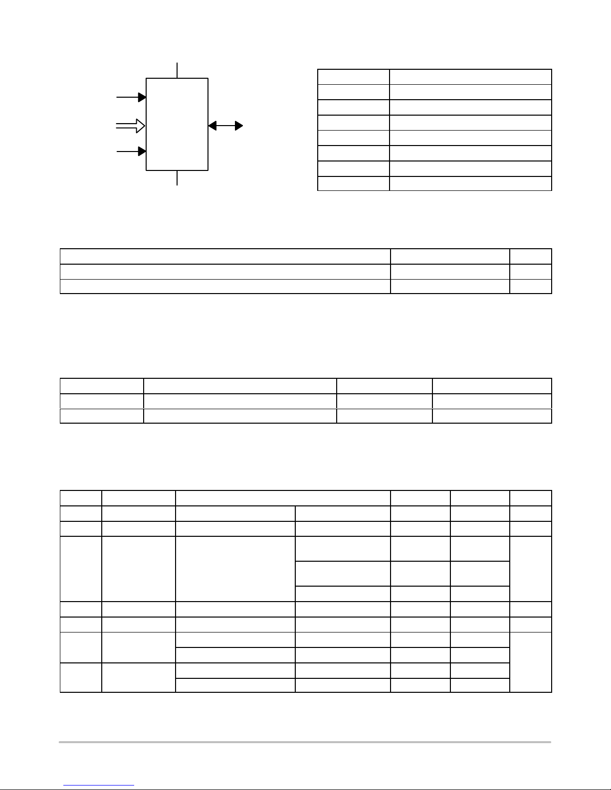
Pin Description
SCL: The Serial Clock input pin accepts the Serial Clock
generated by the Master.
SDA: The Serial Data I/O pin receives input data and
transmits data stored in EEPROM. In transmit mode, this pin
is open drain. Data is acquired on the positive edge, and is
delivered on the negative edge of SCL.
A0, A1 and A2: The Address inputs set the device address
when cascading multiple devices. When not driven, these
pins are pulled LOW internally.
WP: The Write Protect input pin inhibits all write
operations, when pulled HIGH. When not driven, this pin is
pulled LOW internally.
Functional Description
The CAT24Cxx supports the Inter−Integrated Circuit
(I2C) Bus data transmission protocol, which defines a device
that sends data to the bus as a transmitter and a device
receiving data as a receiver. Data flow is controlled by a
Master device, which generates the serial clock and all
START and STOP conditions. The CAT24Cxx acts as a
Slave device. Master and Slave alternate as either
transmitter or receiver.
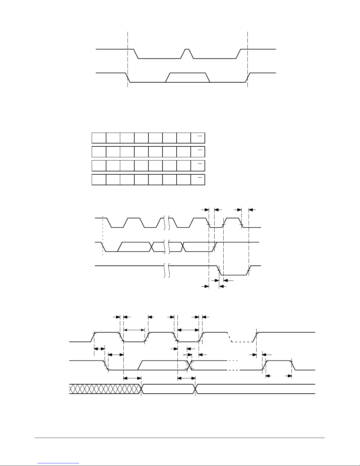
I2C Bus Protocol
The I2C bus consists of two ‘wires’, SCL and SDA. The
two wires are connected to the VCC supply via pull−up
resistors. Master and Slave devices connect to the 2−wire
bus via their respective SCL and SDA pins. The transmitting
device pulls down the SDA line to ‘transmit’ a ‘0’ and
releases it to ‘transmit’ a ‘1’.
Data transfer may be initiated only when the bus is not
busy (see AC Characteristics).
During data transfer, the SDA line must remain stable
while the SCL line is high. An SDA transition while SCL is
high will be interpreted as a START or STOP condition
(Figure 2). The START condition precedes all commands. It
consists of a HIGH to LOW transition on SDA while SCL
is HIGH. The START acts as a ‘wake−up’ call to all
receivers. Absent a START, a Slave will not respond to
commands. The STOP condition completes all commands.
It consists of a LOW to HIGH transition on SDA while SCL
is HIGH.
NOTE: The I/O pins of CAT24Cxx do not obstruct the SCL
and SDA lines if the VCC supply is switched off. During
power−up,the SCL and SDA pins (connected with pull−up
resistors to VCC) will follow the VCC monotonically from
VSS (0 V) to nominal VCC value, regardless of pull−up
resistor value. The delta between the VCC and the
instantaneous voltage levels during power ramping will be
determined by the relation between bus time constant
(determined by pull−up resistance and bus capacitance) and
actual VCC ramp rate.
Device Addressing
The Master initiates data transfer by creating a START
condition on the bus. The Master then broadcasts an 8−bit
serial Slave address. For normal Read/Write operations, the
first 4 bits of the Slave address are fixed at 1010 (Ah). The
next 3 bits are used as programmable address bits when
cascading multiple devices and/or as internal address bits.
The last bit of the slave address, R/W, specifies whether a
Read (1) or Write (0) operation is to be performed. The 3
address space extension bits are assigned as illustrated in
Figure 3. A2, A1and A0must match the state of the external
address pins, and a10, a9and a8are internal address bits.
Acknowledge
After processing the Slave address, the Slave responds
with an acknowledge (ACK) by pulling down the SDA line
during the 9th clock cycle (Figure 4). The Slave will also
acknowledge the address byte and every data byte presented
in Write mode. In Read mode the Slave shifts out a data byte,
and then releases the SDA line during the 9th clock cycle. As
long as the Master acknowledges the data, the Slave will
continue transmitting. The Master terminates the session by
not acknowledging the last data byte (NoACK) and by
issuing a STOP condition. Bus timing is illustrated in
Figure 5.

CAT24C01, CAT24C02, CAT24C04, CAT24C08, CAT24C16
http://onsemi.com
5
START
CONDITION
STOP
CONDITION
SDA
SCL
Figure 2. Start/Stop Timing
1010a10 a9a8R/W CAT24C16
1010A2a9a8R/W CAT24C08
1010A2A1a8R/W CAT24C04
1010A2A1A0R/W CAT24C01 and CAT24C02
Figure 3. Slave Address Bits
189
START
SCL FROM
MASTER
BUS RELEASE DELAY (TRANSMITTER) BUS RELEASE DELAY
(RECEIVER)
DATA OUTPUT
FROM TRANSMITTER
DATA OUTPUT
FROM RECEIVER
ACK DELAY (vtAA)
ACK SETUP (wtSU:DAT)
Figure 4. Acknowledge Timing
SCL
SDA IN
SDA OUT
tBUF
Figure 5. Bus Timing
tSU:STO
tSU:DAT
tDH
tR
tLOW
tAA
tHD:DAT
tHIGH
tLOW
tHD:SDA
tF
tSU:STA

CAT24C01, CAT24C02, CAT24C04, CAT24C08, CAT24C16
http://onsemi.com
6
WRITE OPERATIONS
Byte Write
In Byte Write mode, the Master sends the START
condition and the Slave address with the R/W bit set to zero
to the Slave. After the Slave generates an acknowledge, the
Master sends the byte address that is to be written into the
address pointer of the CAT24Cxx. After receiving another
acknowledge from the Slave, the Master transmits the data
byte to be written into the addressed memory location. The
CAT24Cxx device will acknowledge the data byte and the
Master generates the STOP condition, at which time the
device begins its internal Write cycle to nonvolatile memory
(Figure 6). While this internal cycle is in progress (tWR), the
SDA output will be tri−stated and the CAT24Cxx will not
respond to any request from the Master device (Figure 7).
Page Write
The CAT24Cxx writes up to 16 bytes of data in a single
write cycle, using the Page Write operation (Figure 8). The
Page Write operation is initiated in the same manner as the
Byte Write operation, however instead of terminating after
the data byte is transmitted, the Master is allowed to send up
to fifteen additional bytes. After each byte has been
transmitted the CAT24Cxx will respond with an
acknowledge and internally increments the four low order
address bits. The high order bits that define the page address
remain unchanged. If the Master transmits more than sixteen
bytes prior to sending the STOP condition, the address
counter ‘wraps around’ to the beginning of page and
previously transmitted data will be overwritten. Once all
sixteen bytes are received and the STOP condition has been
sent by the Master, the internal Write cycle begins. At this
point all received data is written to the CAT24Cxx in a single
write cycle.
Acknowledge Polling
The acknowledge (ACK) polling routine can be used to
take advantage of the typical write cycle time. Once the stop
condition is issued to indicate the end of the host’s write
operation, the CAT24Cxx initiates the internal write cycle.
The ACK polling can be initiated immediately. This
involves issuing the start condition followed by the slave
address for a write operation. If the CAT24Cxx is still busy
with the write operation, NoACK will be returned. If the
CAT24Cxx has completed the internal write operation, an
ACK will be returned and the host can then proceed with the
next read or write operation.
Hardware Write Protection
With the WP pin held HIGH, the entire memory is
protected against Write operations. If the WP pin is left
floating or is grounded, it has no impact on the operation of
the CAT24Cxx. The state of the WP pin is strobed on the last
falling edge of SCL immediately preceding the first data
byte (Figure 9). If the WP pin is HIGH during the strobe
interval, the CAT24Cxx will not acknowledge the data byte
and the Write request will be rejected.
Delivery State
The CAT24Cxx is shipped erased, i.e., all bytes are FFh.
ADDRESS
BYTE
DATA
BYTE
SLAVE
ADDRESS
S
A
C
K
A
C
K
A
C
K
S
T
O
P
P
S
T
A
R
T
BUS ACTIVITY:
MASTER
SLAVE
* For the CAT24C01 a7= 0
a7−a0d7−d0
Figure 6. Byte Write Sequence

CAT24C01, CAT24C02, CAT24C04, CAT24C08, CAT24C16
http://onsemi.com
7
tWR
STOP
CONDITION
START
CONDITION
ADDRESS
ACK8th Bit
Byte n
SCL
SDA
Figure 7. Write Cycle Timing
A
C
K
A
C
K
A
C
K
S
T
O
P
S
A
C
K
A
C
K
S
T
A
R
T
P
SLAVE
ADDRESS
n = 1
P v15
ADDRESS
BYTE n n+1 n+P
BUS ACTIVITY:
MASTER
SLAVE
DATA
BYTE DATA
BYTE DATA
BYTE
Figure 8. Page Write Sequence
1891 8
a7a0d7d0
tSU:WP
tHD:WP
ADDRESS
BYTE
DATA
BYTE
SCL
SDA
WP
Figure 9. WP Timing

CAT24C01, CAT24C02, CAT24C04, CAT24C08, CAT24C16
http://onsemi.com
8
READ OPERATIONS
Immediate Read
Upon receiving a Slave address with the R/W bit set to ‘1’,
the CAT24Cxx will interpret this as a request for data
residing at the current byte address in memory. The
CAT24Cxx will acknowledge the Slave address, will
immediately shift out the data residing at the current address,
and will then wait for the Master to respond. If the Master
does not acknowledge the data (NoACK) and then follows
up with a STOP condition (Figure 10), the CAT24Cxx
returns to Standby mode.
Selective Read
Selective Read operations allow the Master device to
select at random any memory location for a read operation.
The Master device first performs a ‘dummy’ write operation
by sending the START condition, slave address and byte
address of the location it wishes to read. After the
CAT24Cxx acknowledges the byte address, the Master
device resends the START condition and the slave address,
this time with the R/W bit set to one. The CAT24Cxx then
responds with its acknowledge and sends the requested data
byte. The Master device does not acknowledge the data
(NoACK) but will generate a STOP condition (Figure 11).
Sequential Read
If during a Read session, the Master acknowledges the 1st
data byte, then the CAT24Cxx will continue transmitting
data residing at subsequent locations until the Master
responds with a NoACK, followed by a STOP (Figure 12).
In contrast to Page Write, during Sequential Read the
address count will automatically increment to and then
wrap−around at end of memory (rather than end of page). In
the CAT24C01, the internal address count will not wrap
around at the end of the 128 byte memory space.
SCL
SDA 8th Bit
STOPNO ACKDATA OUT
89
SLAVE
ADDRESS
S
A
C
K
D ATA
BYTE
N
O
A
C
K
S
T
O
P
P
S
T
A
R
T
BUS ACTIVITY:
MASTER
SLAVE
Figure 10. Immediate Read Sequence and Timing
SLAVE
S
A
C
K
N
O
A
C
K
S
T
O
P
P
S
T
A
R
T
S
A
C
K
SLAVE
ADDRESS
A
C
K
S
T
A
R
T
D ATA
BYTE
ADDRESS
BYTEADDRESS
BUS ACTIVITY:
MASTER
SLAVE
Figure 11. Selective Read Sequence
S
T
O
P
P
SLAVE
ADDRESS
A
C
K
A
C
K
A
C
K
N
O
A
C
K
A
C
K
D ATA
BYTE
n
D ATA
BYTE
n+1
D ATA
BYTE
n+2
D ATA
BYTE
n+x
BUS ACTIVITY:
MASTER
SLAVE
Figure 12. Sequential Read Sequence

CAT24C01, CAT24C02, CAT24C04, CAT24C08, CAT24C16
http://onsemi.com
9
PACKAGE DIMENSIONS
PDIP−8, 300 mils
CASE 646AA
ISSUE A
E1
D
A
L
eb
b2
A1
A2
E
eB
c
TOP VIEW
SIDE VIEW END VIEW
PIN # 1
IDENTIFICATION
Notes:
(1) All dimensions are in millimeters.
(2) Complies with JEDEC MS-001.
SYMBOL MIN NOM MAX
A
A1
A2
b
b2
c
D
e
E1
L
0.38
2.92
0.36
6.10
1.14
0.20
9.02
2.54 BSC
3.30
5.33
4.95
0.56
7.11
1.78
0.36
10.16
eB 7.87 10.92
E 7.62 8.25
2.92 3.80
3.30
0.46
6.35
1.52
0.25
9.27
7.87

CAT24C01, CAT24C02, CAT24C04, CAT24C08, CAT24C16
http://onsemi.com
10
PACKAGE DIMENSIONS
SOIC 8, 150 mils
CASE 751BD
ISSUE O
E1 E
A
A1
h
θ
L
c
eb
D
PIN # 1
IDENTIFICATION
TOP VIEW
SIDE VIEW END VIEW
Notes:
(1) All dimensions are in millimeters. Angles in degrees.
(2) Complies with JEDEC MS-012.
SYMBOL MIN NOM MAX
θ
A
A1
b
c
D
E
E1
e
h
0º 8º
0.10
0.33
0.19
0.25
4.80
5.80
3.80
1.27 BSC
1.75
0.25
0.51
0.25
0.50
5.00
6.20
4.00
L0.40 1.27
1.35

CAT24C01, CAT24C02, CAT24C04, CAT24C08, CAT24C16
http://onsemi.com
11
PACKAGE DIMENSIONS
TSSOP8, 4.4x3
CASE 948AL
ISSUE O
E1 E
A2
A1
e
b
D
c
A
TOP VIEW
SIDE VIEW END VIEW
q1
L1 L
Notes:
(1) All dimensions are in millimeters. Angles in degrees.
(2) Complies with JEDEC MO-153.
SYMBOL
θ
MIN NOM MAX
A
A1
A2
b
c
D
E
E1
e
L1
0º 8º
L
0.05
0.80
0.19
0.09
0.50
2.90
6.30
4.30
0.65 BSC
1.00 REF
1.20
0.15
1.05
0.30
0.20
0.75
3.10
6.50
4.50
0.90
0.60
3.00
6.40
4.40

CAT24C01, CAT24C02, CAT24C04, CAT24C08, CAT24C16
http://onsemi.com
12
PACKAGE DIMENSIONS
MSOP 8, 3x3
CASE 846AD
ISSUE O
E1E
A2
A1 e b
D
c
A
TOP VIEW
SIDE VIEW END VIEW
L1
L2
L
DETAIL A
DETAIL A
Notes:
(1) All dimensions are in millimeters. Angles in degrees.
(2) Complies with JEDEC MO-187.
SYMBOL MIN NOM MAX
q
θ
A
A1
A2
b
c
D
E
E1
e
L
0º 6º
L2
0.05
0.75
0.22
0.13
0.40
2.90
4.80
2.90
0.65 BSC
0.25 BSC
1.10
0.15
0.95
0.38
0.23
0.80
3.10
5.00
3.10
0.60
3.00
4.90
3.00
L1 0.95 REF
0.10
0.85

CAT24C01, CAT24C02, CAT24C04, CAT24C08, CAT24C16
http://onsemi.com
13
PACKAGE DIMENSIONS
TDFN8, 2x3
CASE 511AK
ISSUE A
PIN#1
IDENTIFICATIO
N
E2
E
A3
ebD
A2
TOP VIEW SIDE VIEW BOTTOM VIEW
PIN#1 INDEX AREA
FRONT VIEW
A1
A
L
D2
Notes:
(1) All dimensions are in millimeters.
(2) Complies with JEDEC MO-229.
SYMBOL MIN NOM MAX
A 0.70 0.75 0.80
A1 0.00 0.02 0.05
A3 0.20 REF
b 0.20 0.25 0.30
D 1.90 2.00 2.10
D2 1.30 1.40 1.50
E 3.00
E2 1.20 1.30 1.40
e
2.90
0.50 TYP
3.10
L 0.20 0.30 0.40
A2 0.45 0.55 0.65

CAT24C01, CAT24C02, CAT24C04, CAT24C08, CAT24C16
http://onsemi.com
14
PACKAGE DIMENSIONS
TSOT−23, 5 LEAD
CASE 419AE
ISSUE O
E1 E
A2
A1
e
b
D
c
A
TOP VIEW
SIDE VIEW END VIEW
L1
LL2
Notes:
(1) All dimensions are in millimeters. Angles in degrees.
(2) Complies with JEDEC MO-193.
SYMBOL
θ
MIN NOM MAX
q
A
A1
A2
b
c
D
E
E1
e
L
0º 8º
L1
L2
0.01
0.80
0.30
0.12
0.30
0.05
0.87
0.15
2.90 BSC
2.80 BSC
1.60 BSC
0.95 TYP
0.40
0.60 REF
0.25 BSC
1.00
0.10
0.90
0.45
0.20
0.50

CAT24C01, CAT24C02, CAT24C04, CAT24C08, CAT24C16
http://onsemi.com
15
PACKAGE DIMENSIONS
TSOP−5
CASE 483−02
ISSUE H
NOTES:
1. DIMENSIONING AND TOLERANCING PER
ASME Y14.5M, 1994.
2. CONTROLLING DIMENSION: MILLIMETERS.
3. MAXIMUM LEAD THICKNESS INCLUDES
LEAD FINISH THICKNESS. MINIMUM LEAD
THICKNESS IS THE MINIMUM THICKNESS
OF BASE MATERIAL.
4. DIMENSIONS A AND B DO NOT INCLUDE
MOLD FLASH, PROTRUSIONS, OR GATE
BURRS.
5. OPTIONAL CONSTRUCTION: AN
ADDITIONAL TRIMMED LEAD IS ALLOWED
IN THIS LOCATION. TRIMMED LEAD NOT TO
EXTEND MORE THAN 0.2 FROM BODY.
DIM MIN MAX
MILLIMETERS
A3.00 BSC
B1.50 BSC
C0.90 1.10
D0.25 0.50
G0.95 BSC
H0.01 0.10
J0.10 0.26
K0.20 0.60
L1.25 1.55
M0 10
S2.50 3.00
123
54 S
A
G
L
B
D
H
C
J
__
0.7
0.028
1.0
0.039
ǒmm
inchesǓ
SCALE 10:1
0.95
0.037
2.4
0.094
1.9
0.074
*For additional information on our Pb−Free strategy and soldering
details, please download the ON Semiconductor Soldering and
Mounting Techniques Reference Manual, SOLDERRM/D.
SOLDERING FOOTPRINT*
0.20
5X
CAB
T0.10
2X
2X T0.20
NOTE 5
T
SEATING
PLANE
0.05
K
M
DETAIL Z
DETAIL Z

CAT24C01, CAT24C02, CAT24C04, CAT24C08, CAT24C16
http://onsemi.com
16
PACKAGE DIMENSIONS
UDFN8, 2x3 EXTENDED PAD
CASE 517AZ
ISSUE O
0.065 REF
Copper Exposed
E2
D2
L
E
PIN #1 INDEX AREA
PIN #1
IDENTIFICATION
DAP SIZE 1.8 x 1.8
DETAIL A
D
A1
be
A
TOP VIEW SIDE VIEW
FRONT VIEW
DETAIL A
BOTTOM VIEW
A3
0.065 REF
0.0 - 0.05A3
Notes:
(1) All dimensions are in millimeters.
(2) Refer JEDEC MO-236/MO-252.
SYMBOL MIN NOM MAX
A 0.45 0.50 0.55
A1 0.00 0.02 0.05
A3 0.127 REF
b 0.20 0.25 0.30
D 1.95 2.00 2.05
D2 1.35 1.40 1.45
E 3.00
E2 1.25 1.30 1.35
e
2.95
0.50 REF
3.05
L 0.25 0.30 0.35
A

CAT24C01, CAT24C02, CAT24C04, CAT24C08, CAT24C16
http://onsemi.com
17
PACKAGE DIMENSIONS
WLCSP4, 0.84x0.86
CASE 567DC
ISSUE D
SEATING
PLANE
0.10 C
NOTES:
1. DIMENSIONING AND TOLERANCING PER ASME
Y14.5M, 1994.
2. CONTROLLING DIMENSION: MILLIMETERS.
3. DATUM C, THE SEATING PLANE, IS DEFINED BY
THE SPHERICAL CROWNS OF THE CONTACT
BALLS.
4. COPLANARITY APPLIES TO SPHERICAL CROWNS
OF THE CONTACT BALLS.
5. DIMENSION b IS MEASURED AT THE MAXIMUM
CONTACT BALL DIAMETER PARALLEL TO DATUM C.
2X
DIM
A
MIN MAX
0.28
MILLIMETERS
A1
D0.84 BSC
E
b0.16 0.20
e0.40 BSC
0.38
ÈÈ
ÈÈ
D
EAB
PIN A1
REFERENCE
e
0.05 C
4X b
12
B
A
0.10 C
A1
A2
C
0.08 0.12
0.86 BSC
0.10 C
2X TOP VIEW
SIDE VIEW
BOTTOM VIEW
NOTE 4
e
A2 0.23 REF
PITCH 0.18
4X
DIMENSIONS: MILLIMETERS
*For additional information on our Pb−Free strategy and soldering
details, please download the ON Semiconductor Soldering and
Mounting Techniques Reference Manual, SOLDERRM/D.
SOLDERING FOOTPRINT*
0.40
0.40
RECOMMENDED
A1 PACKAGE
OUTLINE
PITCH
NOTE 3
A
NOTE 5
A
M
0.10 BC
DETAIL A
A3* 0.025 REF
* Die Coat (Optional)
DETAIL A
A2
A
A3*
* Die Coat
(Optional)

CAT24C01, CAT24C02, CAT24C04, CAT24C08, CAT24C16
http://onsemi.com
18
PACKAGE DIMENSIONS
WLCSP5, 0.86x0.84
CASE 567DD
ISSUE C
SEATING
PLANE
0.10 C
NOTES:
1. DIMENSIONING AND TOLERANCING PER ASME
Y14.5M, 1994.
2. CONTROLLING DIMENSION: MILLIMETERS.
3. DATUM C, THE SEATING PLANE, IS DEFINED BY THE
SPHERICAL CROWNS OF THE CONTACT BALLS.
4. COPLANARITY APPLIES TO SPHERICAL CROWNS
OF THE CONTACT BALLS.
5. DIMENSION b IS MEASURED AT THE MAXIMUM CON-
TACT BALL DIAMETER PARALLEL TO DATUM C.
2X
DIM
A
MIN MAX
0.29
MILLIMETERS
A1
D0.86 BSC
E
b0.14 0.18
e0.30 BSC
0.39
ÈÈ
D
EAB
PIN A1
REFERENCE
e
0.05 C
5X b
13
C
A
0.10 C
A1
A
C
0.10 0.14
0.84 BSC
0.10 C
2X TOP VIEW
SIDE VIEW
BOTTOM VIEW
e1
A2 0.23 REF
PITCH 0.16
5X
DIMENSIONS: MILLIMETERS
*For additional information on our Pb−Free strategy and soldering
details, please download the ON Semiconductor Soldering and
Mounting Techniques Reference Manual, SOLDERRM/D.
SOLDERING FOOTPRINT*
0.52
0.30
RECOMMENDED
A1 PACKAGE
OUTLINE
PITCH
NOTE 3
A2
NOTE 4
A
M
0.10 BC
e1 0.52 BSC
PIN A1
REFERENCE
B
2
5X

CAT24C01, CAT24C02, CAT24C04, CAT24C08, CAT24C16
http://onsemi.com
19
Ordering Information
CAT24C01 Ordering Information
Device Order Number
Specific
Device Marking
Package
Type
Temperature
Range (Note 9)
Lead
Finish Shipping
CAT24C01TDI−GT3 MM TSOT−23−5 Industrial NiPdAu Tape & Reel, 3,000 Units / Reel
CAT24C01VP2I−GT3* EE TDFN−8 Industrial NiPdAu Tape & Reel, 3,000 Units / Reel
CAT24C01WI−GT3 24C01WI SOIC−8 Industrial NiPdAu Tape & Reel, 3,000 Units / Reel
CAT24C01WE−GT3 24C01WI SOIC−8 Extended NiPdAu Tape & Reel, 3,000 Units / Reel
CAT24C01YI−GT3 C01 TSSOP−8 Industrial NiPdAu Tape & Reel, 3,000 Units / Reel
CAT24C01YE−GT3 C01 TSSOP−8 Extended NiPdAu Tape & Reel, 3,000 Units / Reel
CAT24C01ZI−GT3 ABMK MSOP−8 Industrial NiPdAu Tape & Reel, 3,000 Units / Reel
CAT24C02 Ordering Information (Notes 10, 11)
Device Order Number
Specific
Device Marking
Package
Type
Temperature
Range (Note 9)
Lead
Finish Shipping
CAT24C02WI−G 24C02H SOIC−8 Industrial NiPdAu Tube, 100 Units / Tube
CAT24C02WI−GA 24C02H SOIC−8 Industrial NiPdAu Tube, 100 Units / Tube
CAT24C02WI−GT3 24C02H SOIC−8 Industrial NiPdAu Tape & Reel, 3,000 Units / Reel
CAT24C02WI−GT3A 24C02H SOIC−8 Industrial NiPdAu Tape & Reel, 3,000 Units / Reel
CAT24C02WE−GT3 24C02H SOIC−8 Extended NiPdAu Tape & Reel, 3,000 Units / Reel
CAT24C02WE−GT3A 24C02H SOIC−8 Extended NiPdAu Tape & Reel, 3,000 Units / Reel
CAT24C02YI−G C02H TSSOP−8 Industrial NiPdAu Tube, 100 Units / Tube
CAT24C02YI−GA C02H TSSOP−8 Industrial NiPdAu Tube, 100 Units / Tube
CAT24C02YI−GT3 C02H TSSOP−8 Industrial NiPdAu Tape & Reel, 3,000 Units / Reel
CAT24C02YI−GT3A C02H TSSOP−8 Industrial NiPdAu Tape & Reel, 3,000 Units / Reel
CAT24C02YE−GT3 C02H TSSOP−8 Extended NiPdAu Tape & Reel, 3,000 Units / Reel
CAT24C02YE−GT3A C02H TSSOP−8 Extended NiPdAu Tape & Reel, 3,000 Units / Reel
CAT24C02VP2I−GT3* C1T TDFN−8 Industrial NiPdAu Tape & Reel, 3,000 Units / Reel
CAT24C02VP2IGT3A* C1T TDFN−8 Industrial NiPdAu Tape & Reel, 3,000 Units / Reel
CAT24C02VP2E−GT3* C1T TDFN−8 Extended NiPdAu Tape & Reel, 3,000 Units / Reel
CAT24C02VP2EGT3A* C1T TDFN−8 Extended NiPdAu Tape & Reel, 3,000 Units / Reel
CAT24C02ZI−GT3 C1 MSOP−8 Industrial NiPdAu Tape & Reel, 3,000 Units / Reel
CAT24C02ZE−GT3 C1 MSOP−8 Extended NiPdAu Tape & Reel, 3,000 Units / Reel
CAT24C02ZI−GT3A C1 MSOP−8 Industrial NiPdAu Tape & Reel, 3,000 Units / Reel
CAT24C02ZE−GT3A C1 MSOP−8 Extended NiPdAu Tape & Reel, 3,000 Units / Reel
CAT24C02TDI−GT3 C1 TSOT−23−5 Industrial NiPdAu Tape & Reel, 3,000 Units / Reel
CAT24C02TDE−GT3 C1 TSOT−23−5 Extended NiPdAu Tape & Reel, 3,000 Units / Reel
CAT24C02TDI−GT3A C1 TSOT−23−5 Industrial NiPdAu Tape & Reel, 3,000 Units / Reel
CAT24C02TDE−GT3A C1 TSOT−23−5 Extended NiPdAu Tape & Reel, 3,000 Units / Reel
CAT24C02LI−GA 24C02H PDIP−8 Industrial NiPdAu Tube, 50 Units / Tube
CAT24C02LE−GA 24C02H PDIP−8 Extended NiPdAu Tube, 50 Units / Tube
CAT24C02HU4IGT3A C1U UDFN8−EP Industrial NiPdAu Tape & Reel, 3,000 Units / Reel
CAT24C02HU4EGT3A C1U UDFN8−EP Extended NiPdAu Tape & Reel, 3,000 Units / Reel
CAT24C02TSI−T3 C1 TSOP−5 Industrial Matte−Tin Tape & Reel, 3,000 Units / Reel
9. Industrial temperature range is −40°C to +85°C and Extended temperature range is −40°C to +125°C.
10.Part numbers ending with “A” for the CAT24C02 are for Gresham (Product Rev H) only die.
11. The CAT24C02 ”non−A” Device Order Numbers use Gresham die (Rev H) for date codes, starting August 1st, 2012. Therefore the Specific
Device Marking for these OPNs reflect Rev H die.
* The TDFN (VP2) package is not recommended for new designs.

CAT24C01, CAT24C02, CAT24C04, CAT24C08, CAT24C16
http://onsemi.com
20
CAT24C04 Ordering Information
Device Order Number
Specific
Device Marking
Package
Type
Temperature
Range (Note 12)
Lead
Finish Shipping
CAT24C04WI−G 24C04K SOIC−8 Industrial NiPdAu Tube, 100 Units / Tube
CAT24C04WI−GT3 24C04K SOIC−8 Industrial NiPdAu Tape & Reel, 3,000 Units / Reel
CAT24C04WE−GT3 24C04K SOIC−8 Extended NiPdAu Tape & Reel, 3,000 Units / Reel
CAT24C04YI−G C04K TSSOP−8 Industrial NiPdAu Tube, 100 Units / Tube
CAT24C04YI−GT3 C04K TSSOP−8 Industrial NiPdAu Tape & Reel, 3,000 Units / Reel
CAT24C04YE−GT3 C04 TSSOP−8 Extended NiPdAu Tape & Reel, 3,000 Units / Reel
CAT24C04VP2I−GT3* C2T TDFN−8 Industrial NiPdAu Tape & Reel, 3,000 Units / Reel
CAT24C04LI−G 24C04K PDIP−8 Industrial NiPdAu Tube, 50 Units / Tube
CAT24C04LE−G 24C04K PDIP−8 Extended NiPdAu Tube, 50 Units / Tube
CAT24C04ZI−GT3 C2 MSOP−8 Industrial NiPdAu Tape & Reel, 3,000 Units / Reel
CAT24C04ZE−GT3 C2 MSOP−8 Extended NiPdAu Tape & Reel, 3,000 Units / Reel
CAT24C04C4ATR 4 WLCSP−4 Industrial N/A Tape & Reel, 5,000 Units / Reel
CAT24C04C5ATR 4 WLCSP−5 Industrial N/A Tape & Reel, 5,000 Units / Reel
CAT24C04TDI−GT3 C2 TSOT−23−5 Industrial NiPdAu Tape & Reel, 3,000 Units / Reel
CAT24C04TDE−GT3 C2 TSOT−23−5 Extended NiPdAu Tape & Reel, 3,000 Units / Reel
CAT24C04HU4I−GT3 C2U UDFN8−EP Industrial NiPdAu Tape & Reel, 3,000 Units / Reel
CAT24C04HU4E−GT3 C2U UDFN8−EP Extended NiPdAu Tape & Reel, 3,000 Units / Reel
CAT24C08 Ordering Information
Device Order Number
Specific
Device Marking
Package
Type
Temperature
Range (Note 12)
Lead
Finish Shipping
CAT24C08WI−G 24C08K SOIC−8 Industrial NiPdAu Tube, 100 Units / Tube
CAT24C08WI−GT3 24C08K SOIC−8 Industrial NiPdAu Tape & Reel, 3,000 Units / Reel
CAT24C08WE−GT3 24C08K SOIC−8 Extended NiPdAu Tape & Reel, 3,000 Units / Reel
CAT24C08YI−G C08K TSSOP−8 Industrial NiPdAu Tube, 100 Units / Tube
CAT24C08YI−GT3 C08K TSSOP−8 Industrial NiPdAu Tape & Reel, 3,000 Units / Reel
CAT24C08YE−GT3 C08 TSSOP−8 Extended NiPdAu Tape & Reel, 3,000 Units / Reel
CAT24C08VP2I−GT3* C3T TDFN−8 Industrial NiPdAu Tape & Reel, 3,000 Units / Reel
CAT24C08VP2E−GT3* C3T TDFN−8 Extended NiPdAu Tape & Reel, 3,000 Units / Reel
CAT24C08LI−G 24C08K PDIP−8 Industrial NiPdAu Tube, 50 Units / Tube
CAT24C08LE−G 24C08K PDIP−8 Extended NiPdAu Tube, 50 Units / Tube
CAT24C08ZI−GT3 C3 MSOP−8 Industrial NiPdAu Tape & Reel, 3,000 Units / Reel
CAT24C08ZE−GT3 C3 MSOP−8 Extended NiPdAu Tape & Reel, 3,000 Units / Reel
CAT24C08C4ATR 8 WLCSP−4 Industrial N/A Tape & Reel, 5,000 Units / Reel
CAT24C08C4CTR** 8 WLCSP−4 Industrial N/A Tape & Reel, 5,000 Units / Reel
CAT24C08C5ATR 8 WLCSP−5 Industrial N/A Tape & Reel, 5,000 Units / Reel
CAT24C08TDI−GT3 C3 TSOT−23−5 Industrial NiPdAu Tape & Reel, 3,000 Units / Reel
CAT24C08TDE−GT3 C3 TSOT−23−5 Extended NiPdAu Tape & Reel, 3,000 Units / Reel
CAT24C08HU4I−GT3 C3U UDFN8−EP Industrial NiPdAu Tape & Reel, 3,000 Units / Reel
CAT24C08HU4E−GT3 C3U UDFN8−EP Extended NiPdAu Tape & Reel, 3,000 Units / Reel
12.Industrial temperature range is −40°C to +85°C and Extended temperature range is −40°C to +125°C.
* The TDFN (VP2) package is not recommended for new designs.
** CAT24C08C4CTR is a backside coated version. Contact factory for other densities.
This manual suits for next models
4
Table of contents
Other ON Semiconductor Semiconductor manuals