Panasonic Z-421V Quick start guide

Technical Guide
Colour Television
Z-421V Chassis
Circuit Description
Panasonic European Television Division
Matsushita Electric (U.K.) Ltd
Order No. TG-990904

3DQDVRQLF
2
Contents
1 CIRCUIT DESCRIPTION...........................................................................................................................3
1.1 SMALL SIGNAL PART .................................................................................................................................3
1.1.1 Tuner and IF output Tuner:.............................................................................................................3
1.1.2 Vision IF ..........................................................................................................................................3
1.1.3 Sound...............................................................................................................................................8
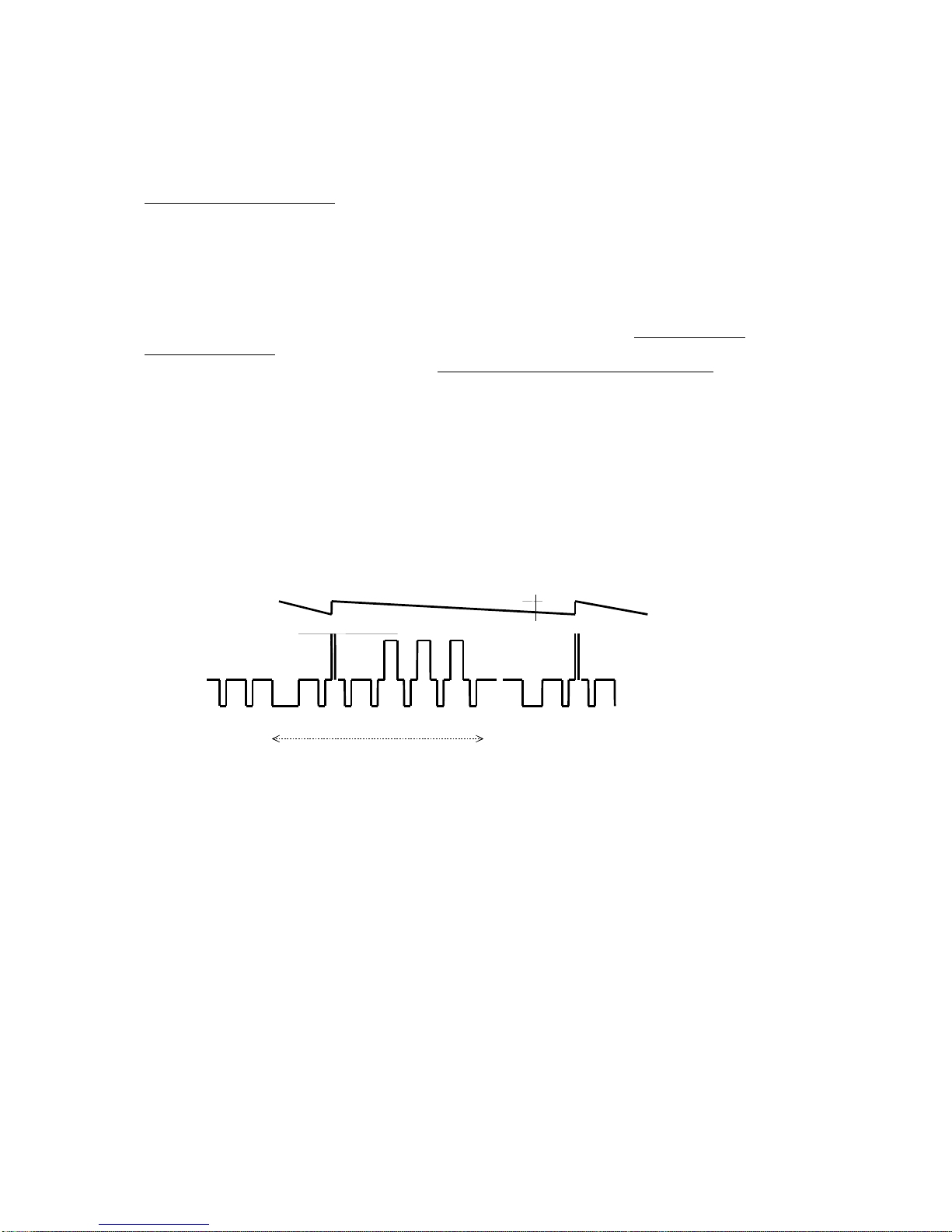
1.1.4 Horizontal and vertical synchronization .......................................................................................10
1.1.5 Luminance and chrominance signal processing............................................................................13
1.1.6 Color Decoder...............................................................................................................................15
1.1.7 AFC - Tuning - ATS .......................................................................................................................18
1.2 DIGITAL CONTROL SIGNALS....................................................................................................................20
1.2.1 1-3-1 local keyboard......................................................................................................................20
1.2.2 1-3-2 IR remote control code.........................................................................................................20
1.2.3 I2C bus...........................................................................................................................................22
1.3 HORIZONTAL DEFLECTION - FBT ...........................................................................................................24
1.3.1 General description:......................................................................................................................24
1.3.2 Horizontal deflection.....................................................................................................................24
1.4 VERTICAL DEFLECTION...........................................................................................................................29
1.4.1 Z-421 circuit ..................................................................................................................................29
1.4.2 Drive circuit part...........................................................................................................................30
1.5 VIDEO AMPLIFIER AND ABS...................................................................................................................32
1.5.1 Video output amplification.............................................................................................................32
1.5.2 ABS operation................................................................................................................................34
1.5.3 Beam current limiter......................................................................................................................35
1.5.4 Euro-scart......................................................................................................................................36
1.6 POWER SUPPLY STR-S5707....................................................................................................................37
1.6.1 Vin terminal, start-up circuit..........................................................................................................37
1.6.2 Oscillator, F/B terminal voltage (pin 7).........................................................................................37
1.6.3 Function of INH terminal (pin 6), control of off-time....................................................................37
1.6.4 Drive circuit...................................................................................................................................37
1.6.5 OCP function.................................................................................................................................37
1.6.6 Latch Circuit..................................................................................................................................38
1.6.7 Thermal shutdown circuit..............................................................................................................38
1.6.8 Over-voltage protection circuit......................................................................................................38
1.6.9 Stand-by Mode TOP210.................................................................................................................38
1.6.10 CONTROL PIN (pin4)...................................................................................................................38
2 VCR PART...................................................................................................................................................39
2.1 KEY FEATURES OF VIDEO IC AND ITS RELATIVES....................................................................39
2.2 RECORD AND PLAYBACK PROCESSING CIRCUIT .....................................................................40
2.2.1 RECORD PROCESSING...............................................................................................................40
2.2.2 PLAYBACK PROCESSING...........................................................................................................43
2.2.3 AUDIO SIGNAL PROCESSING (LA71511M) ..............................................................................46

3DQDVRQLF
3
1 Circuit Description
1.1 Small signal part
1.1.1 Tuner and IF output Tuner:
Type TV standard PIF Channel coverage
B/G 38.9 MHz
L/L’ 38.9 MHz
DT5-BF15P
(DAEWOO) I 38.9 MHz
VHF_L : CH E2 -- CH S7
VHF_H : CH S8 -- CH S36
UHF : CH S37 -- CH E69
The RF tuner selects the picture and sound signals of the desired station by converting the RF signal
into the Intermediate Frequency (IF) of the receiver.
The common UHF/VHF input is realized by an aerial connector (75Ω) (DIN IEC jack). The IF output is
balanced (75Ω). The tuning mode is voltage synthesis.
IF output and SAW filter
The high gain tuner, balanced output can be connected directly to tile SAW filter input.
The surface Acoustic Wave filters are based on the interference of mechanical surface waves.
TV standard B/G L/L’ I
Picture carrier 38.9 MHz 38.9 MHz 38.9 MHz
Color carrier 34.47 MHz 34.47 MHz 34.47 MHz
Sound carrier 33.4 MHz 33.4 MHz 33.4 MHz
1.1.2 Vision IF
See also the related block diagram as well as the diagrams at the end of the report.
The main functions are:
* IF amplifier
* PLL-demodulator and alignment free VCO
* Video buffer
* AFC
* AGC
* Tuner AGC
* Video identification
These functions will be described next in this section.
The TDA884X includes an integrated vision-IF. This gives advantages compared to a stand alone IC
for vision-IF only. Some advantages are:
I
2C bus commands are available for many control functions and alignment. This saves a pins and
external components.
Optimal performance is achieved by means of timing/gating signals derived from the
synchronization part.
Build-in accuracy of circuits is derived by use of the available chroma crystal oscillator.

3DQDVRQLF
4
* IF-amplifier
The IF-amplifier has symmetrical inputs and consists of three AC coupled differential gain stages with
AGC function. Due to the AC coupling, biasing is simple so that cascades can be used and no DC
feedback is necessary. The gain control range of the IF amplifier is 64dB minimal. The input sensitivity
for AGC onset is 70 mV typical. The maximal IF-gain can be reduced with 20dB by means of I²C bus
IFS.
* PLL-demodulator and alignment free VCO
The IF-signal is demodulated with the help of a PLL detector. The PLL detector is used to regenerate a
reference signal that is in phase to the IF-carrier signal. Demodulation is achieved by multiplying this
reference signal with the incoming IF-signal. This reference signal is a clean signal that does not
contain video information; this bandwidth (approx. 60kHz) is determined by the PLL loopfilter pin 5.
The demodulator can handle both negative and negative modulation, selection is done with I²C bus bit
MOD.
A low pass filter after the demodulator output reduces the higher frequency demodulation products.
The voltage controlled oscillator, VCO, is alignment free and makes the concept even more attractive.
No external coil is required any more. It saves both the coil costs and an alignment. As regards EMC
the system becomes more robust. The required IF-system frequency 38.9, 45.75MHz, including
SECAM-L’, is selected by I²C. The correct VCO frequency is determined by the calibrator system
which uses one of the actual chroma crystal as reference. Calibration occurs automatically after
power-on and every time after loss of sync lock (I2C bit SL)
The PLL catching range is plus/min 1MHz around the selected IF-frequency. Within this range the PLL
ensures automatic tracking to the incoming frequency. The PLL is basically an "FPLL", Frequency
Phase Lock Loop system. This extra frequency detector gives an output signal to the PLL loopfilter as
long as a difference in frequency is detected. This ensures fast catching.
The PLL loopfilter time constant can be made fast via Fast Filter IF-PLL, FFI. This function has been
made available to handle RF-transmitter signals with large phase modulation (for special market
areas).
* Video buffer
The video buffer is required to provide a low ohmic video output with the right amplitude and to protect
this output for the occurrence of noise peaks, refer to figure below. The video buffer also contains a
level shifter and gain stage for positive and negative modulation in order to provide a correct video
amplitude and DC level.
The video buffer bandwidth is typical 9 MHz. The video output amplitude is 2.2Vpp (sync inclusive),
independent of the supply voltage. A white spot clamp prevents the video amplitude becoming greater
than 5.3V typical. A noise clamp prevents the video output becoming less than 1.7V typical. (Top sync
is approx. 2V) For strong signal only, the noise peak is inverted to black level.
zero level white spot clamp
top white
zero levelnoise inv. clamptop sync.
1
2
3
4
5
Video out
[V]
Negative Positive
Fig 1: Video signal for negative and positive modulation
The IF part can be switched-off by means of I²C bus command VSW. The internal CVBS input than
can be used (with minimum components) as external input, for instance for satellite.

3DQDVRQLF
5
* AGC
An AGC system controls the IF amplifier gain such that the video output amplitude is constant.
The demodulated video signal is supplied, via a low pass filter, to an AGC detector with external
decoupling capacitor. The AGC detector voltage controls directly the IF gain stages.
Negative/positive modulation:
For optimal AGC behavior the charge and discharge current of the AGC are chosen so that both, a
relative fast AGC, as well a low tilt are possible for positive and negative modulated signals with the
same AGC capacitor.
A SECAM-L speed-up circuit improves the AGC settling time after IF-signal loss.
With tilt is mend the video amplitude variation due to less "memory" function of the AGC capacitor). In
Fig 2 the tilt is given during a field period for positive modulated signals. For negative modulated
signals the tilt is line frequent. For negative modulated signals the AGC is a top sync detector.
Positive modulation:
For positive modulated signals the AGC is a top white AGC including black level clamp which making
the video amplitude independent of video contents.
A top white AGC requires a 100% white reference pulse in order to be independent of video contents.
Suitable for that purpose is the white pulse (Video Insertion Test Signal, VITS) in line 17 and 330 - see
Fig 2.
Because the time constant is large (AGC current is decreased for positive modulation) the AGC will be
independent of the video contents between the reference pulses.
The maximum tilt per field is defined by the external capacitor, the AGC steepness and the small
discharge current in this mode.
//
one field
100% white
tilt
AGC voltage
Reference
pulse Video output
signal
Fig 2: Positive modulated signal with top white reference pulse
This top white AGC however is not optimal for those signals that have neither a white reference pulse
or white video information (e.g. with some VCR signals). Due to the top level AGC principle a gray
scene becomes white and a dark scene becomes gray, see Fig 3. This behavior can be avoided by
means of the black level clamp.

3DQDVRQLF
6
Original video signal
with/without ref. pulse Demodulated signal on video output
Not optimal behaviour Optimal behaviour
Ref
pulse
100%
Ref pulse 100%, luma 50%
Ref pulse, top white<100%
50%
100%
50%
a
100%
Top white AGC only
b
Ref
pulse
100%
Top white AGC
Black clamp AGC
50%
100%
50%
c
Fig 3: Top white and black clamp AGC
The Fig 3 “b” shows that the video amplitude is increased by the top white AGC, such that 100% white
is obtained. As a consequence the black level increases also.
The black level clamp AGC in “c” prevents this behavior and becomes automatically active if the video
black level on the video output increases.
In the external mode only the top white AGC is active. The black clamp AGC than is switched off
because the internal signal is not synchronized any more to the horizontal oscillator.
SECAM-L speed-up circuit:
In case of positive modulation and large reduction of the incoming IF-input level a speed-up circuit is
needed. This because the AGC action is slow since the AGC discharge current is small (450nA), for
minimizing the tilt.
The speed-up circuit measures the amplitude of the video output signal and will react after
approximately 60ms if the video output is continuously below 80% white level.
If the speed-up is activated the AGC capacitor will be discharged with a current of 50mA.
* Tuner AGC
The tuner AGC is provided to reduce the tuner gain and thus the tuner output voltage when receiving
strong RF signals. The tuner AGC takes over when the IF input reaches a certain input level, that can
be adjusted by I²C function AGC take over.
The tuner gain can be reduced by means of the open collector output pin 54.
* AFC
AFC output information is available for search tuning. With the alignment free concept this AFC
information is very accurate and derived via a counter. The AFC output is available by the I²C bus
outputs AFA, AFB.
The AFC window width can be increased by means of I²C bus AFW. This allows bigger frequency
steps during search tuning.
Notice: AFC information is updated once a field during the vertical retrace and only valid when the
coincidence detector is in-lock (SL=1)
* Video identification
The IF-part includes a stand-alone video identification circuit. This makes the ident function
independent of the sync part. The ident output is available by I²C bus, IFI, and can be used during
search tuning and for automatic sound mute in full scart application.
The video ident circuit measures the main frequency of the input signal, which should be
approximately 16kHz.The video ident. can be connected to the "internal" video signal or to the
selected CVBS input signal.

3DQDVRQLF
7
IF Amplifier
VCO
PLL
FFl FastFilter IF
Tuner
take over
adjust
MOD
Gating
AGC
detector LPF
LPF
Demodulator
Calibrator
AFC
IFA, IFB, IFC
IF frequency selection
AFW
AFA
AFB
fsc
MOD
pos. / Neg. VSW
Video mute
Video
Ident
IF1
PLLloopfilter
AGCdecoupling
N.C.
IF input 1
IF input 2
Tuner AGCout
IF Video out
4
3
48
49
54
53
6
5
Fig 4 : Block diagram: Vision IF

3DQDVRQLF
8
1.1.3 Sound
See also the related block diagram as well as the diagrams at the end of the report.
The main functions are:
* Limiter
* PLL-Demodulator
* Pre-amplifier and mute
* Audio switch
* Volume controlled amplifier
These functions will be described next.
* Limiter
The sound carrier signal is supplied to this limiter input via an external bandpass filter. This external
bandpass filter is used for selectivity, the internal filter at the pin is used for noise reduction. The limiter
consists of AC coupled amplifier stages. The minimum input amplitude for limiting is typical 1mVrms.
The input impedance is 8K5 in parallel with 5pF.
* PLL-Demodulator
Sound demodulation is achieved by a PLL FM-demodulator and does not need any external
alignment.
The PLL has been optimized for a low S/N ratio with still an acceptable power consumption. The PLL
catching range is 4.2 - 6.8MHz, which is suitable for all multistandard applications.
* Pre-amplifier and mute
The pre-amplifier output signal available at the deemphasis pin can be used for SCART application. At
this pin the deemphasis capacitor has to be connected. The output level is 500mVrms for a FM swing
of 50kHz.
A pre-amplifier with DC feedback has been provided. The DC component of the deemphasis signal is
always 3V, also during sound mute. Sound mute plop is therefore minimized.
When no video signal is identified the deemphasis output is automatically muted.
* Audio switch
An audio switch has been provided for full SCART function. The audio switch is controlled by the I2C
bus Source Select INA/INC. For positive modulation, MOD, the external sound input is automatically
selected for an external AM sound demodulator.
* Volume controlled amplifier
The volume control is active for both internal and external audio signals. The nominal gain is +9dB and
minimal -71dB, which gives a total control range of 80dB minimal.

3DQDVRQLF
9
Limiter
Sound decoupling
AVLdecoupling
Ext. audio in
1
2
45
56
15
55
AVL
-6dB
0 / -6dB
LPF
BPF
PLLdemodulator
Loopfilter Pre-amplifier
Audio
switch
AVLVolumeFAV
Fixed audio
INA, INB
INC, MOD
XA= 0: 0dB
XA= 1: -6dB
VCO
Automatic volume level
Volume control
1 - 10MHz
15k
3V
+15dB
-71dB
500mVrms
max. 2Vrms
500mVrms @ 50kHz swep
250mVrms @ 25kHz sweep
AVLfeature not
on all models
Sound mute:
INTmode via: SL = 0, SM = 1
EXTmode via: IFl = 0, SM = 1
STB= 0 ; SM = 1
No mute ; VIM = 1
Sound IF in Deemphasis /
Audio line-out
Audio out
Fig 5: Block diagram: Sound

3DQDVRQLF
10
1.1.4 Horizontal and vertical synchronization
See also the related block diagram as well as the diagrams at the end of the report.
The main functions are:
* Horizontal sync separator
* Horizontal oscillator and calibration system
* PHI-1 detector
* PHI-2 detector and sandcastle generation
* Horizontal output with slow start/stop facility
* Coincidence detector
* Noise detector
* Vertical sync separator
* Vertical divider system
* Horizontal sync separator
The horizontal sync separator is supplied from the CVBS/Y inputs (chosen video source). For
horizontal synchronization the sync separator slices in the middle of the sync pulse and the slicing
level is independent of the sync pulse amplitude. For the vertical synchronization the sync pulse is
sliced at a level of about 30% (closer to the black level). This ensures optimal output signals for a
stable horizontal and vertical deflection under various video input conditions.
The top sync level is clamped at the CVBS input. The black level is stored internally.
* Horizontal oscillator and calibration system
The horizontal oscillator requires no external components and is fully integrated. The adjustment for
nominal frequency is derived automatically by a calibration circuit.
The oscillator generates a sawtooth signal with double horizontal frequency. This sawtooth signal is
used to derive several other gating and timing signals. After calibration the horizontal oscillator is
controlled by the PHI-1 loop for synchronization with the incoming video input signal.
The calibrator is responsible for the automatic adjustment of the horizontal oscillator. One of the color
crystals is being used as reference. For that reason a correct crystal selection by XA,XB (Xtal
selection) is very important during power-on. Calibration occurs during the vertical retrace period and
only under following conditions:
- At power-on/ initialization
- After power dip (shutdown detection), re-initialization is required.
- After loss of synchronization (e.g. after channel switching)
* PHI-1 detector
The PHI-1 detector is a PLL circuit that synchronizes the horizontal oscillator with the incoming video
signal. The PLL compares the output of the H-sync separator with the horizontal oscillator. The PLL
output current is converted to a voltage by means of the external loop filter. This voltage controls the
horizontal oscillator. The loop filter is connected externally so the time constant can be defined
according to the customer requirements. Because the static loop gain is very high there will be no
phase shift when switching between input signals with different line.
* PHI-2 detector and sandcastle
As described, the Horizontal PLL (PHI-1 loop) synchronizes the horizontal oscillator with the incoming
video signal. The PHI-2 loop provides a stable picture position on screen.
This is necessary because due to beam current variations the storage time of the line transistor varies
and, due to that, the picture position on screen.
The PHI-2 detector compares the horizontal oscillator signal (reference) with the horizontal flyback
input pulse, pin 41. This flyback pulse is related to the horizontal deflection.
The PHI-2 circuit shifts the horizontal drive, pin 40, such that the picture position on screen is constant.
The flyback input pin 41 is combined with the sandcastle output. This combined function provides a
three level sandcastle signal and is available starting with the highest level: burstkey, line blanking (=
flyback pulse) and vertical blanking.
The phase of the video signal with respect to the deflection current can be adapted by I²C bus HS
(horizontal shift, shift picture left/right).
The PHI-2 loop filter is a first order filter. The capacitor is connected externally on pin 42.

3DQDVRQLF
11
* H-output and slow start/stop
The horizontal output is the driver pin for the line deflection. It is an open collector output. Under
normal operation condition the duty cycle of the output pulse is 45% off (Hout = high) / 55% on (Hout =
low).
A build in slow start/stop circuit ensures a smooth start/stop behavior of the line deflection and protects
the line output transistor.
During switch-on the horizontal output starts with the double frequency (31.25 kHz) and with a duty
cycle of 75% off (Hout = high)/ 25% on (Hout = low). After about 50ms the frequency is changed to the
normal value (15.625 kHz) and the duty cycle to 45% off (Hout = high) / 55% on (Hout = low).
Also during switching-off via stand by (STB) the frequency is switched to the double value and the
RGB drive is set to maximum to discharge the voltage on the EHT capacitor to half of its maximum
value. After about 100ms the RGB drive is set to minimum and 50ms later the horizontal drive is
switched-off.
* Noise detector
The TDA8844 has an internal noise detector which is used to switch the time constant of the horizontal
PLL.
The input of the detector is connected to the selected CVBS input.
The noise detector measures the RMS value of the noise during a part of the sync pulse. (The
detection level is 100mVrms and corresponds to 20dB S/N-ratio for 1Vpp CVBS).
A field counter is used for hysteresis and decides after 2 successive fields whether noise is detected.
When noise is detected the horizontal PLL time constant is switched to slow.
* Coincidence detector
The coincidence detector detects whether the incoming CVBS signal is synchronized with the
horizontal oscillator, thus whether the PHI-1 loop is in-lock. The output is available by I²C bus, SL, and
can be used for search tuning and OSD. For out of lock condition the coincidence detector can be
made less sensitive (about 5 dB) by control bit STM (search tuning mode). This prevents false stops.
* Vertical sync separator
The vertical sync separator separates the vertical sync pulse from the composite sync signal. This
separated sync pulse is used to trigger the vertical divider system. To generate a trigger pulse for the
divider the minimum pulse width of the incoming vertical sync pulse must be 17µs.
The integrator network is designed such that for anticopy signals (e.g. Macrovision) with vertical
pulses of 10µs (on) and 22µs (off) still a vertical sync pulse is generated. (Because more lines with
vertical pulses are present, pulse width of less than 17µs is allowed, by integration still the required
level is reached).
* Vertical divider system
The divider system uses a counter that delivers the timing for the vertical ramp generator in the
geometry processor. The clock is derived from the horizontal line oscillator.
The divider system synchronizes on the vertical sync pulse of the vertical sync separator.
The divider has three modes of operation:
1. Search mode (large window)
This mode is activated when the circuit is not synchronized or when a non-standard signal is received.
In the search mode the divider can catch between about 45 and 64.5Hz.
2. Standard mode (narrow window)
This mode is switched on (coming from search mode) when more than 15 successive vertical sync
pulses are detected in the narrow window. When the circuit is in the standard mode and a vertical sync
pulse is missing the retrace of the vertical ramp generator is started at the end of the window (thus
automatic insertion of missing vertical sync pulses). As consequence the disturbance of the picture is
very small. The circuit will switch back to the search window when 6 succeeding vertical periods no
sync pulses are found within the window. (See also NCIN below)
In the narrow window mode the PHI-1 is inhibited during the vertical egalization pulses to prevent
disturbance.

3DQDVRQLF
12
3. Standard TV-norm: divider ratio 525 (60Hz) or 625 (50Hz)
When the system is switched to the narrow window (standard mode) it is checked whether the
incoming vertical sync pulses are according to the TV norm, if so IVW=1. When 15 standard TV-norms
are counted the divider system is switched to the standard divider ratio mode. In this mode the divider
is always reset at the standard value even if the vertical sync pulse is missing.
The system switches back to the narrow window when 3 vertical sync pulses are missed. When also
in the narrow window 3 vertical sync pulses are missed, the divider will switch to the search window
mode.
As described above the vertical divider needs some waiting time before switching back to the search
window mode. When a fast reaction is required for instance during channel switching the system can
be forced to the search window by means of I²C bus, setting NCIN = 1 (vertical divider mode).
Immediate after forcing to search mode NCIN has to be set back to 0 for optimum performance.
The vertical synchronization mode of operation can be selected by I²C bus FORF/S, forced field
frequency.
Furthermore, 50/60Hz identification is available by I²C bus FSI (50/60Hz), and norm signal
identification with IVW. Interlace can be switched on and off by I²C bus DL.
PHl1 Filter
42
41
40
Timing
PHl1
Hout
Calibration
Horizontal
Flyback in /
detector Horizontal
oscillator PHl2
detector Slow start
&Stop
system
Vertical
Divider Sandcastle
Generator
Vsync.
separation
separation
Hsync.
Noise
detector
Coincidence
detector
Blanking
Generator
slow start
&stop
+
-
6V
HBL, LBM
HOB
IVW
FSI
HSH
FORF, FORS
NCIN, DL
Hsync
Hsync
Fsc
Luma
from
Filters &
Switches
Vertical pulse
for geometry
Sandcastle out
Drive
PHl2 Filter
VID
POC
FOA
FOBIF1
43
RGBblank 1
Fig 6 : Block diagram: Horizontal and vertical synchronization

3DQDVRQLF
13
1.1.5 Luminance and chrominance signal processing
* Chrominance signal processing
For chroma signal processing, the selected signal is supplied to both the PAL/NTSC chroma bandpass
filter and the SECAM cloche filter via a variable gain amplifier which is controlled by ACC and ACL
detection circuits.
The dynamic range of the ACC is 26dB and detects only the burst amplitude; consequently the burst
signal at the bandpass/cloche filter input is constant for a burst signal range +6dB -> -20dB where 0dB
= 300mVPP burst.
The ACL is a chroma amplitude detector and is active when the chroma/burst ratio exceeds
approximately 3. It ensures that CVBS signal to chroma bandpass & cloche filter is limited for large
chroma/burst ratios (>3). which results in a constant saturation for such non-standard transmissions.
The ACL is independent of the ACC; it controls only the chroma amplitude and does not influence the
color burst sensitivity. The ACL function can be switched on/off via bus command ACL.
The output signal of the chroma bandpass circuit is supplied to the PAL/NTSC decoder and the output
signal of the cloche filter is supplied to the SECAM decoder for further chroma processing.
* Luminance signal processing
For luminance processing, the selected video signal is supplied to the H/Vsync circuits for sync
processing and also to an adjustable delay line (0ns - 320ns, minimum step is 40ns, controlled via bus
bits YD0-YD3). The chroma trap is bypassed for no burst transmissions when in own intelligence
mode (automode). In Y/C modes the video signal follows a direct path with 160ns delay so as to
ensure similarity with chroma path delay. The output signal is supplied to the peaking and coring
stages whose operation is illustrated below.
The peaking function is realized with τ= 160ns delay cells (i.e. frequency response reaches a
maximum at a frequency f = 1/2τ= 3.125MHz).
The coring function has a non-linear transfer characteristic which implies that a noise suppression
range (coring range) of 15 IRE is realized. This means that extra noise introduced due to increased
gain of the peaking amplifier is defeated by the coring function. The coring stage is activated via the
I²C bus (COR).
Asymmetric peaking is introduced to enhance picture definition. The negative/positive overshoot ratio
is approximately 1.8. The degree of peaking is controlled by the peaking amplifier via the I²C bus
(PEAKING). The output of the peaking amplifier is summed with the delayed (160ns) selected video
signal (see Fig 7).
The output of the peaking/coring stages (i.e. output of summing stage) is fed as internal luminance
signal (YINT) to the YUV selection circuit (see YUV/RGB processing part).
SUMMING
STAGE 25IRE
100IRE
45IRE
Nominal PEAKING
PEAK
ASSYMETRIC
PEAKING
CORING
FUNCTION
COR
PEAKING
FUNCTION
15IRE
100IRE
(b1/wh)
Selected
VIDEO
Signal DELAY
160ns
25IRE
45IRE
50IRE50IRE
Fig 7: Peaking and coring operation

3DQDVRQLF
14
CS1, CS0
38
CVBS &
Y/C
select
output
select
Peaking
&
Coring
burst
detect
chroma
detect
CVBS Buffer
INA, INB, INC
0 - 320nS
160nS
CVBS
Y/ C
Chroma trap
no burst in auto mode
INA, INB
INC
To Sync.
Luma
Chroma
ACC
ACL
Cloche
Chroma (SECAM)
Fsc
Filter Tuning
Chroma (PAL/ NTSC)
COR
Peaking
CB
ACL
YD0 - YD3
(26)
11
10
13
17
CVBS1
out
Chroma
CVBS2
out
CVBS / Y
CVBS int.
CVBS ext.
Fig 8 : Block diagram: Filters and CVBS/Y/C switches

3DQDVRQLF
15
1.1.6 Color Decoder
See also the related block diagram as well as the diagrams at the end of the report.
The main functions are:
* PLL/VCXO
* PAL/NTSC identification
* SECAM identification
* ASM ( Automatic System Manager )
* (R-Y)/(B-Y) demodulation
* PLL/VCXO
The PLL operates during the burstkey period; it generates a VCXO reference signal ( fVCXO ), in
phaselock with the incoming burst signal ( fBURST ). Prior to lock condition, the signals fVCXO and fBURST
are not synchronous and are present at phase detector input. The loop filter averages the phase
detector output current and the resulting control signal to the VCXO is proportional to Sin(2π∆ft) where
∆f = fVCXO - fBURST.
A lock situation occurs when ∆f < VCXO holding range; once in lock, the phase detector output current
is proportional to θE = θVCXO - θBURST (θEis the static phase error).
The combined phase detector and VCXO sensitivity is high to ensure a small static phase error.
For fast color acquisition, the phase detector is in high gain mode when a color system is not yet
identified.
The VCXO loop (not to be confused with phase locked loop, PLL) compensates for any attenuation
loss or phase shift in the crystal so that the it’s loop gain is unity and loop phase shift is zero. The
VCXO reference outputs (0° and 90°) are stable sinusoids.
VCXO oscillation is at series resonance of the selected Xtal. Since the PLL automatically tunes the
VCXO to the burst (if inside the PLL holding range) fine tuning of the VCXO with a trimming
capacitance is not necessary.
The motional capacitance of the Xtal is damped by the internal resistance of the VCXO pins (i.e. 1K )
in order to realize the holding range.
The catching range (pull-in) of the PLL loop is governed by the PLL loop filter; the loop filter can be
chosen so that PLL holding and catching range are similar (direct catching).
The HUE phase rotator is inoperational when the PLL is active (i.e. no phase rotation during the
burstkey period). Outside the burstkey period, the hue control rotates the VCXO reference phases
from -40°to 40°linearly for I²C bus command (HUE: 0 --> 63), see also device specification.
* PAL/NTSC demodulation
The 0°and 90°reference signals from the VCXO are supplied to the HUE phase rotator; it's outputs
(H0, H90) are supplied to the (B-Y) and (R-Y) burst demodulators respectively.
The demodulated burst from the (B-Y) demodulator supplies NTSC ident information to the ASM (IDN
signal). The demodulated burst from (R-Y) demodulator supplies PAL ident information to the ASM
(IDP signal). For correct demodulation of (R-Y) PAL burst and chroma signals, then the H90 signal
requires 180°phase shift on alternate lines. This is realized with the H/2 switch before the (R-Y)
demodulator. It is not active during demodulation of NTSC signals.
The (B-Y)/(R-Y) baseband signals are obtained from the chroma signal by the (B-Y)/(R-Y)
demodulators, filtered and supplied via the PAL/SECAM switch (PS) to the internal baseband delay
line.
The demodulator gain ratio (B-Y)/(R-Y) is typically 1.78 in order to compensate for scaling in the
transmitter. For NTSC applications it is possible to bypass the delay line via I2C bus command BPS;
the gain is also corrected then by a factor two. The VINT and UINT signals from delay line outputs are fed
to the YUV selection circuit (see YUV/RGB processing part).
* SECAM demodulation
SECAM demodulation is realized with a PLL type demodulator.
When the VCXO is connected to pin 35 (controlled by XTS) and if a 4.43MHz Xtal is present on that
pin then SECAM demodulation is possible. The auto tuning loop, consisting of PLL demodulator and
oscillator, ensures that the PLL oscillator is locked to the 4.43MHz Xtal frequency during calibration
time in the vertical retrace period. The SECAM reference voltage, generated at pin 16, is regulated in
order that the PLL demodulator output is set to a reference voltage derived from a stable bandgap
voltage.
Outside calibration the oscillator remains tracking the SECAM chrominance resulting in the
corresponding demodulated voltage. This is delivered to the LF de-emphasis stage and to the line

3DQDVRQLF
16
ident stage of the Automatic System Manager (IDS signal). The H/2 switch distributes the
demodulated signal to the (R-Y) and (B-Y) amplifiers and via the PAL/SECAM switch (PS) to the
baseband delay line. The bypass mode of the delay line is not possible for SECAM.
The VINT and UINT signals from delay line outputs are fed to the YUV selection circuit (see YUV/RGB
processing part).
* ASM ( Automatic System Manager )
The ASM is field synchronous; it can identify PAL/NTSC/SECAM color standards. The different
possibilities are controlled by the I²C bus input commands (CM2 --> CM0) . These input commands
are communicated to the ASM via the I²C bus.
The I²C bus input commands (XA, XB) , also supplied to the ASM via the I²C bus, indicate which Xtals
must be connected to pins 34 and 35. This is essential for correct calibration of the horizontal
oscillator.
The I2C command FCO disables the color killer in forced modes only and allows maximum color
sensitivity. (see also I²C bus description).
For color identification purposes there is also communication with the ASM and:
- the PAL/NTSC ident circuits (IDP, IDN)
- the SECAM ident (IDS)
- the VCXO via xtalswitch (XTS)
- the PAL/SECAM switch (PS)
- the R-Y demodulator (H/2)
The I²C output commands (SXA, SXB) indicate whether the (XA, XB) bits have been correctly
transmitted by the I²C bus. The I²C output commands (CD2 --> CD0) indicate which color system has
been identified.
* The (B-Y)/(R-Y) demodulation
The (B-Y)/(R-Y) baseband signals are extracted from the chroma signal by the (B-Y)/(R-Y)
demodulators, filtered and supplied via the output switch to pins 29 and 30 respectively. For correct
demodulation of (R-Y) PAL signals, then the demodulated (R-Y) signals requires 180" phase reversal
on alternate lines, this is realized with the PAL switch
The demodulator gain ratio (B-Y)/(R-Y) is typically 1.78 in order to compensate far scaling in the
transmitter. During the line/field blanking periods of the sandcastle pulse the (B-Y)/(R-Y) are blocked ;
then the correct DC levels are supplied to the (B-Y)/(R-Y) outputs.
When SECAM is identified by the SECAM add-on decoder and no PAL/NTSC is already identified by
the ASM, then the ASM sets the (B-Y)/(R-Y) switch open via (DEMSW). This implies that the (B-Y)/(R-
Y) signals from the SECAM decoder can be directly connected to pin 29 and 30 respectively without
extra loading.

3DQDVRQLF
17
36
1H delay
XTAL4.4 / 3.6
Loop filter phase detector
1H delay
HUE
VCXO
phase
rotator
Automatic
System
Manager
Osc.
LF
Deemp.
R-Y
amp.
B-Y
amp.
6dB
6dB
Vint.
Uint.
IDN
B-Y demodulator
R-Y demodulator
SECAMPLL
demodulator
Chroma
SECAM
Chroma
PAL/ NTSC
Fsc
XTS
HUE
H/2
H0H90
BPS
ECMB
PS
IDP
H/2
IDS
IDN
IDP
IDS
XTS
PS H/2
XA, XB, FCO
CM2-CM0SXA, SXB
CD2-CD0
35 34 33
XTAL3.6
SECAMdecoupling
16
Fsc
Fig 9 : Block diagram: Color decoder

3DQDVRQLF
18
1.1.7 AFC - Tuning - ATS
IF VCO tuned circuit
The IF VCO tuned circuit is applied to pin 3 and 4 of the TDA8844. The resonance frequency is two
times the IF-frequency suitable for IF standard of 38.9 MHz. The VCO frequency can be adjusted by
I2C bus, so there is no need to readjust the external coil.
Catching range
The VCO is automatically tracked to the incoming IF frequency when the PLL is in-lock. Within the PLL
catching range (2MHz) the performance of the demodulator is independent of the incoming IF-
frequency (is one of advantages of a PLL-demodulator). Correct VCO adjustment is only required
when the AFC is used.
SECAM L’
For SECAM L’ a frequency shift is made of typical -5.5MHz by means of I2C bus; a capacitor of 10pF
is added to the VCO tuned circuit.
AFC output
The AFC output is available by I2C bus.
The analogue AFC characteristic is derived from the PLL loop-filter pin 5. The figure 10 below gives
the relation with the incoming IF frequency. The digital signals AFA anti AFB are derived form the AFC
slope via comparators
The microcontroller uses these digital AFC signals to :
•drive the main IC for VCO reference frequency adjustment.
•catch the tuning voltage of each program during channel search.
•compensate for IF frequency drift daring normal operation .
2.7 V
3.4 V
2 V
in window outside window
RF too low
outside window
RF too low
above reference below reference
fIF
AFB
AFA
Vpin5
Fig. 10 : AFC Slope and I2C output bits

3DQDVRQLF
19
Automatic Tuning System(ATS)
The Automatic Tuning System initiates a full auto-search of the channel, covering all the bands and
the system available on the TV set. At the end of the search, the microcontroller uses the teletext or
VPS information (when these signals are available ) to find out the TV network name of the channel.
Then the microcontroller sort out the stations.
Each registered TV signal broadcaster is given a Country and Network identification (CNI) code.
These codes are uniquely designated for use by a single broadcast network, by definition. within the
entire world.
In Germany the TV set uses VPS (Video Programming System) signals on video lines 16 and 329 to
pick up the CNI codes of the received signals.
VPS is transmitted in the vertical blanking interval in dedicated TV lines. Transmission is done in
biphase code, and the data contains 15 data words of each 8 bits. The transmission rate is 2.5Mbit/s.
The first 2 of the 15 data words are for synchronization of the receiver and for identification of the data
line. Words 3 and 4 contains a source identification, which is not relevant for VPS.
Word 5 contains a sound identification(mono/dual/stereo sound)
Word 6 displays a program related signal content identification; as is the case for words 7 to 10 it is
not relevant for VPS.
Words 11 to 15 with their 40 bits contain the actual VPS information.
CNI
Word number 13 14
bit number 7 8 1 2 3 4 5 6 7 8
VPS bit
number 5 6 7 8 11 12 13 14 15 16
Code Country code Network or program provider
code
Fig 11 : VPS Data format for words 13 and 14
In UK and France the TV set uses PDC (Program Delivery Control) information from teletext lines. The
CNI code is transported in a number of possible location (hidden from display in teletext program
guide pages or extension data packet type 26, and in program label of extension data packet type 8/30
format 2).
Sorting
Once the channel search is completed, the programs with PDC signals are given a name.
The TV broadcasting stations with a name (that is with PDC signal ) are sorted according to the list
below. The sorting order depends upon the TV signal. the broadcasting system, and reception
conditions If either BBC1. BBC2 or ITV are not located, then their respective pre-allocated Program
positions (1 to 3) will remain unused.

3DQDVRQLF
20
1.2 Digital control signals
1.2.1 1-3-1 local keyboard
The local keyboard is not made in matrix with regular scanning from the microcontroller. Instead one
input of the microcontroller is used to monitor 5 keys. Pressing one key makes the resistance to the
ground vary, and therefore the level at pin 33 of microcontroller
1.2.2 1-3-2 IR remote control code
The IR remote control code used is Philips RC5 code. The RC5 protocol can hand1e up to 4096
commands organized as two sets of 64 commands in up to 32 individually addressable groups, each
of which is allocated to a separate item of equipment.
RC5 remote control transmission protocol:
Bi-phase encoding is used for RC5 code words. As shown in fig. 12 a HIGH to LOW Transition is a
logic 0; one with a LOW to HIGH Transition is a logic 1.
Logic 0
1 bit period
Logic 1
1.7778mS
Fig. 12: bi-phase code
Table of contents
Popular Chassis manuals by other brands

Lutron Electronics
Lutron Electronics Sivoia QS roller 100 installation guide

Texas Instruments
Texas Instruments 990A13 manual

Sun Microsystems
Sun Microsystems Sun Fire B1600 Administration installation guide

BitFenix
BitFenix phenom mini-itx Quick installaion guide

ERECA
ERECA STAGE RACER 2 installation manual

Advantech
Advantech HPC-8224 user manual