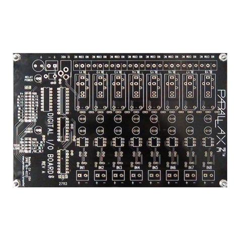
Parallax BASIC Stamp 2e Owner's manual

BASIC Stamp Programming Manual
Version 2.0c

Warranty
Parallax warrants its products against defects in materials and workmanship for a period of 90 days. If you discover a defect,
Parallax will, at its option, repair, replace, or refund the purchase price. Simply call our sales department for an RMA
number, write it on the label and return the product with a description of the problem. We will return your product, or its
replacement, using the same shipping method used to ship the product to Parallax (for instance, if you ship your product via
overnight express, we will do the same).
This warranty does not apply if the product has been modified or damaged by accident, abuse, or misuse.
14-Day Money-Back Guarantee
If, within 14 days of having received your product, you find that it does not suit your needs, you may return it for a refund.
Parallax will refund the purchase price of the product, excluding shipping/handling costs. This does not apply if the
product has been altered or damaged.
Copyrights and Trademarks
Copyright © 2000 by Parallax, Inc. All rights reserved. PBASIC is a trademark and BASIC Stamp is a registered trademark or
Parallax, Inc. PIC is a registered trademark of Microchip Technology, Inc. Windows is a registered trademark of Microsoft
Corporation. 1-wire is a registered trademark of Dallas Semiconductor. Other brand and product names are trademarks or
registered trademarks of their respective holders.
Disclaimer of Liability
Parallax, Inc. is not responsible for special, incidental, or consequential damages resulting from any breach of warranty, or
under any legal theory, including lost profits, downtime, goodwill, damage to or replacement of equipment or property, and
any costs of recovering, reprogramming, or reproducing any data stored in or used with Parallax products.
Internet Access
We maintain Internet systems for your convenience. These may be used to obtain software, communicate with members of
Parallax, and communicate with other customers. Access information is shown below:
Web: http://www.parallaxinc.com
http://www.stampsinclass.com
General e-mail: [email protected]
Tech. e-mail: [email protected]
Internet BASIC Stamp Discussion List
We maintain a BASIC Stamp discussion list for people interested in BASIC Stamps. Many people subscribe to the list, and all
questions and answers to the list are distributed to all subscribers. It’s a fun, fast, and free way to discuss BASIC Stamp
issues. To subscribe to the BASIC Stamps list, visit the Tech Support section of the Parallax, Inc website.
This manual is valid with the following software and firmware versions:
BASIC Stamp 1:
STAMP.EXE software version 2.1
Firmware version 1.4
BASIC Stamp 2:
STAMP2.EXE software version 1.1
STAMPW.EXE software version 1.096
Firmware version 1.0
BASIC Stamp 2e:
STAMP2E.EXE software version 1.0
STAMPW.EXE software version 1.096
Firmware version 1.0
BASIC Stamp 2sx:
STAMP2SX.EXE software version 1.0
STAMPW.EXE software version 1.096
Firmware version 1.0
BASIC Stamp 2p:
STAMP2P.EXE software version 1.6
STAMPW.EXE software version 1.098
Firmware version 1.1
The information herein will usually apply to newer versions but may not apply to older versions. New software can be
obtained free on our ftp and web site (ftp.parallaxinc.com, www.parallaxinc.com). If you have any questions about what
you need to upgrade your product, please contact Parallax.
Contents
BASIC Stamp Programming Manual 2.0c •www.parallaxinc.com •Page 1
PREFIX ........................................................................................................5
INTRODUCTION TO THE BASIC STAMP.........................................................7
BASIC STAMP 1 HARDWARE.........................................................................................8
BASIC STAMP 2 HARDWARE.......................................................................................10
BASIC STAMP 2E HARDWARE.....................................................................................12
BASIC STAMP 2SX HARDWARE...................................................................................14
BASIC STAMP 2P HARDWARE.....................................................................................16
DEVELOPMENT BOARDS...............................................................................................18
BASIC Stamp 1 Carrier Board..............................................................................18
BASIC Stamp 2 Carrier Board..............................................................................19
BASIC Stamp Super Carrier Board......................................................................20
Board of Education.................................................................................................22
BASIC Stamp Activity Board.................................................................................23
GUIDELINES AND PRECAUTIONS...................................................................................25
QUICK START GUIDE.................................................................................29
USING THE BASIC STAMP EDITOR .............................................................33
BASIC STAMP WINDOWS EDITOR...............................................................................34
BASIC STAMP DOS EDITOR .......................................................................................41
BASIC STAMP ARCHITECTURE...................................................................45
RAM ORGANIZATION (BS1).........................................................................................45
RAM ORGANIZATION (BS2, BS2E, BS2SX, BS2P)...................................................46
DEFINING AND USING VARIABLES.................................................................................48
The Rules of Symbol Names................................................................................49
Defining Array Variables........................................................................................51
Aliases and Variable Modifiers..............................................................................53
CONSTANTS AND COMPILE-TIME EXPRESSIONS .........................................................56
NUMBER REPRESENTATIONS .......................................................................................59
ORDER OF OPERATIONS...............................................................................................60
INTEGER MATH RULES..................................................................................................62
UNARY OPERATORS......................................................................................................63
Absolute Value (ABS).............................................................................................64
Cosine (COS)..........................................................................................................64
Decoder (DCD)........................................................................................................64

Contents
Page 2•BASIC Stamp Programming Manual 2.0b •www.parallaxinc.com
Inverse (~)................................................................................................................64
Negative (-)..............................................................................................................64
Encoder (NCD)........................................................................................................65
Sine (SIN)................................................................................................................65
Square Root (SQR)................................................................................................66
BINARY OPERATORS.....................................................................................................66
Add (+)......................................................................................................................67
Subtract (-)...............................................................................................................67
Multiply (*)................................................................................................................67
Multiply High (**).....................................................................................................68
Multiply Middle (*/)..................................................................................................68
Divide (/)...................................................................................................................69
Modulus (//)..............................................................................................................70
Minimum (MIN)........................................................................................................70
Maximum (MAX).....................................................................................................71
Digit (DIG)................................................................................................................72
Shift Left (<<)...........................................................................................................72
Shift Right (>>)........................................................................................................72
Reverse (REV)........................................................................................................73
And (&).....................................................................................................................73
Or (|)..........................................................................................................................73
Xor (^).......................................................................................................................74
And Not (&/).............................................................................................................75
Or Not (|/).................................................................................................................75
Xor Not (^/)...............................................................................................................75
BASIC STAMP COMMAND REFERENCE......................................................77
AUXIO............................................................................................................................81
BRANCH........................................................................................................................83
BUTTON........................................................................................................................85
COUNT..........................................................................................................................89
DATA..............................................................................................................................91
DEBUG..........................................................................................................................97
DTMFOUT....................................................................................................................107
EEPROM......................................................................................................................111
END..............................................................................................................................115
FOR…NEXT................................................................................................................117
FREQOUT....................................................................................................................123
GET..............................................................................................................................127

Contents
BASIC Stamp Programming Manual 2.0c •www.parallaxinc.com •Page 3
GOSUB........................................................................................................................129
GOTO...........................................................................................................................133
HIGH............................................................................................................................135
I2CIN............................................................................................................................137
I2COUT........................................................................................................................143
IF…THEN.....................................................................................................................149
INPUT ..........................................................................................................................155
IOTERM.......................................................................................................................157
LCDCMD......................................................................................................................159
LCDIN ..........................................................................................................................167
LCDOUT ......................................................................................................................171
LOOKDOWN................................................................................................................177
LOOKUP......................................................................................................................183
LOW.............................................................................................................................187
MAINIO ........................................................................................................................189
NAP..............................................................................................................................191
OUTPUT ......................................................................................................................195
OWIN ...........................................................................................................................197
OWOUT .......................................................................................................................205
PAUSE.........................................................................................................................213
POLLIN ........................................................................................................................215
POLLMODE.................................................................................................................219
POLLOUT ....................................................................................................................225
POLLRUN....................................................................................................................231
POLLWAIT...................................................................................................................235
POT..............................................................................................................................239
PULSIN........................................................................................................................241
PULSOUT....................................................................................................................243
PUT..............................................................................................................................245
PWM ............................................................................................................................247
RANDOM.....................................................................................................................251
RCTIME .......................................................................................................................255
READ...........................................................................................................................261
RETURN......................................................................................................................265
REVERSE....................................................................................................................267
RUN .............................................................................................................................269
SERIN..........................................................................................................................273
SEROUT......................................................................................................................293
SHIFTIN.......................................................................................................................309
SHIFTOUT...................................................................................................................313
SLEEP..........................................................................................................................317
SOUND........................................................................................................................319

Contents
Page 4•BASIC Stamp Programming Manual 2.0b •www.parallaxinc.com
STOP...........................................................................................................................321
STOP...........................................................................................................................323
TOGGLE......................................................................................................................327
WRITE..........................................................................................................................329
XOUT...........................................................................................................................333
APPENDIX A: ASCII CHART......................................................................337
APPENDIX B: RESERVED WORDS.............................................................339
APPENDIX C: CONVERSION FORMATTERS...............................................341

Prefix
BASIC Stamp Programming Manual 2.0c •www.parallaxinc.com •Page 5
Thank you for purchasing the Parallax BASIC Stamp development
system. We have done our best to produce a full-featured, yet easy to use
development system for the BASIC Stamp microcontrollers. We hope you
will find this system as enjoyable to use as we do.
This manual is written for the latest available BASIC Stamp modules and
software as of November 2000. As the product-line evolves new
information may become available. It is always recommended to visit the
Parallax, Inc. web site, www.parallaxinc.com, for the latest information.
This manual is intended to be a complete reference manual to the
architecture and command structure of the BASIC Stamps. This manual is
not meant to teach programming or electrical design; though a person can
learn a lot by paying close attention to the details in this book. If you have
never programmed in the BASIC language or are unfamiliar with
electronics, it would be best to locate one or more of the following books
for further information:
1. Programming and Customizing the BASIC Stamp Computer
Scott Edwards, TAB Books ISBN: 0-07-913684-2
2. Microcontroller Projects with BASIC Stamps
Al Williams, R&D Books ISBN: 0-87930-587-8
3. The Microcontroller Application Cookbook
Matt Gilliland, Woodglen Press ISBN: 0-615-11552-7
4. What's A Microcontroller
Free on Parallax CD (Documentation -> Educational Curriculum
section) and web site (Downloads section), or for purchase in print
5. BASIC Analog and Digital
Free on Parallax CD (Documentation -> Educational Curriculum
section) and web site (Downloads section), or for purchase in print
6. Earth Measurements
Free on Parallax CD (Documentation -> Educational Curriculum
section) and web site (Downloads section), or for purchase in print
7. Robotics
Free on Parallax CD (Documentation -> Educational Curriculum
section) and web site (Downloads section), or for purchase in print
In addition, there are hundreds of great examples available on the Parallax
CD and web site (www.parallaxinc.com). Also, Nut & Volts Magazine
(www.nutsvolts.com / 1-800-783-4624) is a national electronic hobbyist's

Prefix
Page 6•BASIC Stamp Programming Manual 2.0b •www.parallaxinc.com
magazine that features monthly articles featuring the BASIC Stamps. This
is an excellent resource for beginners and experts alike! For a sample of the
BASIC Stamp articles, visit their web site.
Packing List
The BASIC Stamps are available in many different forms. You may have
received them in a Starter Kit in a special limited-time package or
individually. The packing list below describes the general list of items that
would be included in a BASIC Stamp Starter Kit at the time of this writing:
BASIC Stamp Starter Kit
•(1) BASIC Stamp Module (Rev. D, BS1-IC, OEMBS1, BS2-IC,
OEMBS2, BS2e-IC, BS2sx-IC or BS2p-IC)
•(1) BASIC Stamp development software (on CD in Software section)
•(1) BASIC Stamp manual (this manual)
•(1) BASIC Stamp development board (Stamp 1 Carrier Board, Stamp
2 Carrier Board, Super Carrier Board, BASIC Stamp Activity
Board or Board or Education)
•(1) Set of jumper wires (only included with Board of Education)
•(1) 9-pin serial cable
If any items are missing, please let us know.

1: Introduction to the BASIC Stamps
BASIC Stamp Programming Manual 2.0c •www.parallaxinc.com •Page 7
Welcome to the wonderful world of BASIC Stamp microntrollers. BASIC
Stamp microcontrollers have been in use by engineers and hobbyists since
we first introduced them in 1992. As of July 2000, Parallax customers have
put more than 200,000 BASIC Stamp modules into use. Over this eight-
year period, the BASIC Stamp line of controllers has evolved into five
models and many physical package types, explained below.
General Operation Theory
BASIC Stamps are microcontrollers (tiny computers) that are designed for
use in a wide array of applications. Many projects that require an
embedded system with some level of intelligence can use a BASIC Stamp
module as the controller.
Each BASIC Stamp comes with a BASIC Interpreter chip, internal memory
(RAM and EEPROM), a 5-volt regulator, a number of general-purpose I/O
pins (TTL-level, 0-5 volts), and a set of built-in commands for math and
I/O pin operations. BASIC Stamps are capable of running a few thousand
instructions per second and are programmed with a simplified, but
customized form of the BASIC programming language, called PBASIC.
PBASIC Language
We developed PBASIC specifically for the BASIC Stamps as a simple, easy
to learn language that is also well suited for this architecture. It includes
many of the instructions featured in other forms of BASIC (GOTO,
FOR...NEXT, IF...THEN) as well as some specialized instructions (SERIN,
PWM, BUTTON, COUNT and DTMFOUT). This manual includes an
extensive section devoted to each of the available instructions.
Hardware
At the time of this writing, there are currently five models of the BASIC
Stamp; the BASIC Stamp 1, BASIC Stamp 2, BASIC Stamp 2e, BASIC
Stamp 2sx and BASIC Stamp 2p. The diagrams below detail the various
package types and part numbers of these modules.

Introduction to the BASIC Stamps
Page 8•BASIC Stamp Programming Manual 2.0b •www.parallaxinc.com
BASIC Stamp 1
Basic Stamp
©1993
REV D
TM
P0
P1
P2
P3
P4
P5
P6
P7
+5V
Vin
+5V
Vss
Vss
Vss
>>
.1“(2.54 mm)
.1“ (2.54 mm)
1.5“(38 mm)
2.5“ (63.5 mm)
.5“(13 mm).5“(13 mm)
Figure 1.1:BASIC Stamp 1 Rev. D
(27100)
Figure 1.2:BASIC Stamp 1 (Rev.
B) (BS1
-IC)
Figure 1.3:OEM BASIC Stamp 1
(Rev. A) (27295 or 27296)
VIN
VSS
PCO
PCI
P0
P1
P2
P3
P4
P5
P6
P7
13
14
1
2
3
4
5
6
7
8
9
10
11
12
BS1-IC
RES
VDD
1.41“ (36 mm)
.4“(10 mm)
.1“ (2.54 mm)
.19“(4.8mm)
V i
n V s
s
P C O P C I
V dd R E S P 0 P 1 P 2 P 3 P 4 P 5 P 6 P 7
1
OEM BASIC Stamp 1
(c) 1999
Rev A
>
>
1
1 1 1
C1 +U3
RN1
XTAL
1.4“ (36 mm)
1
.
4
“
( 3
6
m
m
)
0
.
2
5
“
( 6
m
m
)
0.1“ (2.54 mm)
0
.
1
“
( 2
.
5
4
m
m
)

1: Introduction to the BASIC Stamps
BASIC Stamp Programming Manual 2.0c •www.parallaxinc.com •Page 9
The BASIC Stamp 1 is available in the above three physical packages. The
BASIC Stamp 1 Rev. D (simply called the Rev. D), see Figure 1.1, includes
prototyping area suitable for soldering electronic components. The BS1-IC
(Figure 1.2) uses surface mount components to fit in a small 14-pin SIP
package. The OEMBS1 (Figure 1.3) features an easier-to-trace layout
meant to aid customers who wish to integrate the BASIC Stamp 1 circuit
directly into their design (as a lower-cost solution). The OEMBS1 is
available in either an assembled form or a kit form. All three packages are
functionally equivalent with the exception that the Rev. D does not have
an available reset pin.
Pin Name Description
1VIN Unregulated power in: accepts 5.5 -15 VDC (6-40 VDC on
BS1-IC rev. b), which is then internally regulated to 5 volts. May
be left unconnected if 5 volts is applied to the VDD (+5V) pin.
2VSS System ground: connects to PC parallel port pin 25 (GND) for
programming.
3PCO PC Out: connects to PC parallel port pin 11 (BUSY) for
programming.
4PCI PC In: connects to PC parallel port pin 2 (D0) for programming.
5VDD
5-
volt DC input/output: (Also called +5V) if an unregulated voltage
is applied to the VIN pin, then this pin will output 5 volts. If no
voltage is applied to the VIN pin, then a regulated voltage
between 4.5V and 5.5V should be applied to this pin.
6RES
Reset input/output: goes low when power supply is less than
approximately 4.2 volts, causing the BASIC Stamp to reset. Can
be driven low to force a reset. This pin is internally pulled high
and may be left disconnected if not needed. Do not drive high.
7-14 P0-P7 General-purpose I/O pins: each can sink 25 mA and source 20
mA. However, the total of all pins should not exceed 50 mA (sink)
and 40 mA (source).
See the "BASIC Stamp Programming Connections" section, below, for
more information on the required programming connections between the
PC and the BASIC Stamp.
Table 1.1:BASIC Stamp 1 Pin
Descriptions.

Introduction to the BASIC Stamps
Page 10 •BASIC Stamp Programming Manual 2.0b •www.parallaxinc.com
BASIC Stamp 2
The BASIC Stamp 2 is available in the above two physical packages. The
BS2-IC (Figure 1.4) uses surface mount components to fit in a small 24-pin
DIP package. The OEMBS2 (Figure 1.5) features an easier-to-trace layout
meant to aid customers who wish to integrate the BASIC Stamp 2 circuit
directly into their design (as a lower-cost solution). The OEMBS2 is
available in either an assembled form or a kit form. Both packages are
functionally equivalent.
SOUT
SIN
ATN
VSS
P0
P1
P2
P3
P4
P5
P6
P7
VIN
VSS
RES
VDD
P15
P14
P13
P12
P11
P10
P9
P8
24
23
22
21
20
19
18
17
16
15
14
13
1
2
3
4
5
6
7
8
9
10
11
12
BS2-IC
1.2“(31 mm)
.62“ (16 mm)
.1“(2.54 mm)
Figure 1.4:BASIC Stamp 2
(Rev. E) (BS2
-IC)
Figure 1.5:OEM BASIC Stamp 2
(Rev. A) (27290 or 27291)
Vin
Vss
Vdd
RES
P0
P1
P2
P3
P4
P5
P6
P7
OEM BASIC Stamp 2
(c) 1999 RevA
RN1
Q3
+
XTAL
P8
P9
P10
P11
P12
P13
P14
P15
Q1
U3
Q2
RN2
C3
C2
TM
2.0“(51 mm)
0.25“(6mm)
0.25“ (6 mm)
2.0“ (51 mm)
0.1“ (2.54 mm)

1: Introduction to the BASIC Stamps
BASIC Stamp Programming Manual 2.0c •www.parallaxinc.com •Page 11
Pin Name Description
1SOUT Serial Out: connects to PC serial port RX pin (DB9 pin 2 / DB25
pin 3) for programming.
2SIN Serial In: connects to PC serial port TX pin (DB9 pin 3 / DB25 pin
2) for programming.
3ATN Attention: connects to PC serial port DTR pin (DB9 pin 4 / DB25
pin 20) for programming.
4VSS
System ground: (same as pin 23) connects to PC serial port GND
pin (DB9 pin 5 / DB25 pin 7) for programming.
5-20 P0-P15
General-purpose I/O pins: each can sink 25 mA and source 20
mA. However, the total of all pins should not exceed 50 mA (sink)
and 40 mA (source) if using the internal 5-volt regulator. The
total
per 8-pin groups (P0 –P7 or P8 –15) should not exceed 50 mA
(sink) and 40 mA (source) if using an external 5-volt regulator.
21 VDD
5-volt DC input/output: if an unregulated voltage is applied to the
VIN pin, then this pin will output
5 volts. If no voltage is applied to
the VIN pin, then a regulated voltage between 4.5V and 5.5V
should be applied to this pin.
22 RES
Reset input/output: goes low when power supply is less than
approximately 4.2 volts, causing the BASIC Stamp to reset. Can
be driven low to force a reset. This pin is internally pulled high
and may be left disconnected if not needed. Do not drive high.
23 VSS System ground: (same as pin 4) connects to power supply’s
ground (GND) terminal.
24 VIN Unregulated power in: accepts 5.5 -15 VDC (6-40 VDC on BS2-
IC rev. e), which is then internally regulated to 5 volts. May be left
unconnected if 5 volts is applied to the VDD (+5V) pin.
See the "BASIC Stamp Programming Connections" section, below, for
more information on the required programming connections between the
PC and the BASIC Stamp.
Table 1.2:BASIC Stamp 2 Pin
Descriptions.

Introduction to the BASIC Stamps
Page 12 •BASIC Stamp Programming Manual 2.0b •www.parallaxinc.com
BASIC Stamp 2e
The BASIC Stamp 2e is available in the above two physical packages. The
BS2e-IC (Figure 1.6) uses surface mount components to fit in a small 24-
pin DIP package. The OEMBS2e (Figure 1.7) features an easier-to-trace
layout meant to aid customers who wish to integrate the BASIC Stamp 2e
circuit directly into their design (as a lower-cost solution). The OEMBS2e
is available in assembled form only.
SOUT
SIN
ATN
VSS
P0
P1
P2
P3
P4
P5
P6
P7
VIN
VSS
RES
VDD
P15
P14
P13
P12
P11
P10
P9
P8
24
23
22
21
20
19
18
17
16
15
14
13
1
2
3
4
5
6
7
8
9
10
11
12
BS2e-IC
1.2“(31 mm)
.62“ (16 mm)
.1“(2.54 mm)
Rev A
BS2e
© 2000
1Figure 1.6:BASIC Stamp 2e
(Rev. A) (BS2e
-IC)
Figure 1.7:OEM BASIC Stamp 2e
(Rev A) (27293)
Vin
Vss
Vdd
RES
P0
P1
P2
P3
P4
P5
P6
P7
(c) 2000 Rev A
RN1
Q3
+
XTAL
P8
P9
P10
P11
P12
P13
P14
P15
Q1
Q2
RN2
C3C2
TM
2.0“(51 mm)
0.25“(6mm)
0.25“ (6 mm)
2.0“ (51 mm)
0.1“ (2.54 mm)
C1

1: Introduction to the BASIC Stamps
BASIC Stamp Programming Manual 2.0c •www.parallaxinc.com •Page 13
Pin Name Description
1SOUT Serial Out: connects to PC serial port RX pin (DB9 pin 2 / DB25
pin 3) for programming.
2SIN Serial In: connects to PC serial port TX pin (DB9 pin 3 / DB25 pin
2) for programming.
3ATN Attention: connects to PC serial port DTR pin (DB9 pin 4 / DB25
pin 20) for programming.
4VSS
System ground: (same as pin 23) connects to PC serial port GND
pin (DB9 pin 5 / DB25 pin 7) for programming.
5-20 P0-P15
General-purpose I/O pins: each can source and sink 30 mA.
However, the total of all pins should not exceed 75 mA (source or
sink) if using the internal 5-volt regulator. The total per 8-pin
groups (P0 –P7 or P8 –15) should not exceed 100 mA (source
or sink) if using an external 5-volt regulator.
21 VDD
5-volt DC input/output: if an unregulated voltage is applied to the
VIN pin, then this pin will output 5 volts. If no voltage is applied to
the VIN pin, then a regulated voltage between 4.5V and 5.5V
should be applied to this pin.
22 RES
Reset input/output: goes low when power supply is less than
approximately 4.2 volts, causing the BASIC Stamp to reset. Can
be driven low to force a reset. This pin is internally pulled high
and may be left disconnected if not needed. Do not drive high.
23 VSS System ground: (same as pin 4) connects to power supply’s
ground (GND) terminal.
24 VIN Unregulated power in: accepts 5.5 -12 VDC (7.5 recommended),
which is then internally regulated to 5 volts. May be left
unconnected if 5 volts is applied to the VDD (+5V) pin.
See the "BASIC Stamp Programming Connections" section, below, for
more information on the required programming connections between the
PC and the BASIC Stamp.
Table 1.3:BASIC Stamp 2e Pin
Descriptions.

Introduction to the BASIC Stamps
Page 14 •BASIC Stamp Programming Manual 2.0b •www.parallaxinc.com
BASIC Stamp 2sx
The BASIC Stamp 2sx is available in the above two physical packages.
The BS2sx-IC (Figure 1.8) uses surface mount components to fit in a small
24-pin DIP package. The OEMBS2sx (Figure 1.9) features an easier-to-
trace layout meant to aid customers who wish to integrate the BASIC
Stamp 2sx circuit directly into their design (as a lower-cost solution). The
OEMBS2sx is available in assembled form only.
SOUT
SIN
ATN
VSS
P0
P1
P2
P3
P4
P5
P6
P7
VIN
VSS
RES
VDD
P15
P14
P13
P12
P11
P10
P9
P8
24
23
22
21
20
19
18
17
16
15
14
13
1
2
3
4
5
6
7
8
9
10
11
12
BS2SX-IC
1.2“(31 mm)
.62“ (16 mm)
.1“(2.54 mm)
Figure 1.8:BASIC Stamp 2sx (Rev.
B) (BS2sx
-IC)
Figure 1.9:OEM BASIC Stamp 2sx
(Rev. A) (27294)
Vin
Vss
Vdd
RES
P0
P1
P2
P3
P4
P5
P6
P7
(c) 2000 Rev A
RN1
Q3
+
XTAL
P8
P9
P10
P11
P12
P13
P14
P15
Q1
Q2
RN2
C3C2
TM
2.0“(51 mm)
0.25“(6mm)
0.25“ (6 mm)
2.0“ (51 mm)
0.1“ (2.54 mm)
C4
C1

1: Introduction to the BASIC Stamps
BASIC Stamp Programming Manual 2.0c •www.parallaxinc.com •Page 15
Pin Name Description
1SOUT Serial Out: connects to PC serial port RX pin (DB9 pin 2 / DB25
pin 3) for programming.
2SIN Serial In: connects to PC serial port TX pin (DB9 pin 3 / DB25 pin
2) for programming.
3ATN Attention: connects to PC serial port DTR pin (DB9 pin 4 / DB25
pin 20) for programming.
4VSS System ground: (same as pin 23) connects t
o PC serial port GND
pin (DB9 pin 5 / DB25 pin 7) for programming.
5-20 P0-P15
General-purpose I/O pins: each can source and sink 30 mA.
However, the t
otal of all pins should not exceed 75 mA (source or
sink) if using the internal 5-volt regulator. The total per 8-pin
groups (P0 –P7 or P8 –15) should not exceed 100 mA (source
or sink) if using an external 5-volt regulator.
21 VDD
5-volt DC input/output: if an unregulated voltage is applied to the
VIN pin, then this pin will output 5 volts. If no voltage is applied to
the VIN pin, then a regulated voltage between 4.5V and 5.5V
should be applied to this pin.
22 RES
Reset input/output: goes low when power supply is less than
approximately 4.2 volts, causing the BASIC Stamp to reset. Can
be driven low to force a reset. This pin is internally pulled high
and may be left disconnected if not needed. Do not drive high.
23 VSS System ground: (same as pin 4) connects to power supply’s
ground (GND) terminal.
24 VIN Unregulated power in: accepts 5.5 -12 VDC (7.5 recommended),
which is then internally regulated to 5 volts. May be left
unconnected if 5 volts is applied to the VDD (+5V) pin.
See the "BASIC Stamp Programming Connections" section, below, for
more information on the required programming connections between the
PC and the BASIC Stamp.
Table 1.4:BASIC Stamp 2sx Pin
Descriptions.

Introduction to the BASIC Stamps
Page 16 •BASIC Stamp Programming Manual 2.0b •www.parallaxinc.com
BASIC Stamp 2p
The BASIC Stamp 2p is available in the above two physical packages.
Both packages use surface mount components to fit in a small package.
The BS2p24-IC (Figure 1.10) is a 24-pin DIP package. The BS2p40-IC
(Figure 1.11) is a 40-pin DIP package. Both packages are functionally
equivalent accept that the BS2p40 has 32 I/O pins instead of 16.
SOUT
SIN
ATN
VSS
P0
P1
P2
P3
P4
P5
P6
P7
VIN
VSS
RES
VDD
P15
P14
P13
P12
P11
P10
P9
P8
24
23
22
21
20
19
18
17
16
15
14
13
1
2
3
4
5
6
7
8
9
10
11
12
BS2p24-IC
1.2“(31 mm)
.62“ (16 mm)
.1“(2.54 mm)
Rev A
BS2p 24
© 2000
1
SOUT
SIN
ATN
VSS
P0
P1
P2
P3
P4
P5
P6
P7
VIN
VSS
RES
VDD
X15
X14
X13
X12
X11
X10
X9
X8
BS2p40-IC
2.1“(53 mm)
.62“ (16 mm)
.1“(2.54 mm)
Rev A
BS2p 40
© 2000
1
1
2
3
4
5
6
7
8
9
10
11
12
13
14
15
16
17
18
19
20
40
39
38
37
36
35
34
33
32
31
30
29
28
27
26
25
24
23
22
21
MAIN I/O
AUX I/O
P0
P2
P3
P4
P5
P6
P7
P8
P9
P10
P11
P12
P13
P14
P15
X7
X6
X5
X4
X3
X2
X1
X0
Figure 1.10:BASIC Stamp 2p24
(Rev A) (BS2p24-IC) This module
is identical in function to the
BS2p40-IC, except that it has 16 I/O
pins.
Figure 1.11:BASIC Stamp 2p40
(Rev A) (BS2p40-IC) This module
is identical in function to the
BS2p24-IC, except that it has 32 I/O
pins.

1: Introduction to the BASIC Stamps
BASIC Stamp Programming Manual 2.0c •www.parallaxinc.com •Page 17
Pin Name Description
1SOUT Serial Out: connects to PC serial port RX pin (DB9 pin 2 / DB25
pin 3) for programming.
2SIN Serial In: connects to PC serial port TX pin (DB9 pin 3 / DB25 pin
2) for programming.
3ATN Attention: connects to PC serial port DTR pin (DB9 pin 4 / DB25
pin 20) for programming.
4VSS System ground: (same as pin 23 on BS2p24, or pin 39 on
BS2p40) connects to PC serial port GND pin (DB9 pin 5 / DB25
pin 7) for programming.
5-20 P0-P15
General-purpose I/O pins: each can source and sink 30 mA.
However, the total of all pins (including X0-X15, if using the
BS2p40) should not exceed 75 mA (source or sink) if using the
internal 5-volt regulator. The total per 8-pin groups (P0 –P7, P8
–15, X0 –X7 or X8 –X15) should not exceed 100 mA (source
or
sink) if using an external 5-volt regulator.
{21-36} X0-X15
(BS2p40 Only!) Auxiliary Bank of General-
purpose I/O pins: each
can source and sink 30 mA. However, the total of all pins
(including P0 –P15) should not exceed 75 mA (source or sink) if
using the internal 5-volt regulator. The total per 8-pin groups (P0
–P7, P8 –15, X0 –X7 or X8 –X15) should not exceed 100 mA
(source or sink) if using an external 5-volt regulator.
21 {37} VDD
5-volt DC input/output: if an unregulated voltage is applied to the
VIN pin, then this pin will output 5 volts. If no voltage is applied to
the VIN pin, then a regulated voltage between 4.5V and 5.5V
should be applied to this pin.
22 {38} RES
Reset input/output: goes low when power supply is less than
approximately 4.2 volts, causing the BASIC Stamp to reset. Can
be driven low to force a reset. This pin is internally pulled high
and may be left disconnected if not needed. Do not drive high.
23 {39} VSS System ground: (same as pin 4) connects to power supply’s
ground (GND) terminal.
24 {40} VIN Unregulated power in: accepts 5.5 -12 VDC (7.5 recommended),
which is then internally regulated to 5 volts. May be left
unconnected if 5 volts is applied to the VDD (+5V) pin.
NOTE: Pin numbers in braces {} are BS2p40 pin numbers.
See the "BASIC Stamp Programming Connections" section, below, for
more information on the required programming connections between the
PC and the BASIC Stamp.
Table 1.5:BASIC Stamp 2p Pin
Descriptions.

Introduction to the BASIC Stamps
Page 18 •BASIC Stamp Programming Manual 2.0b •www.parallaxinc.com
Development Boards
We provide a number of development boards to make using the BASIC
Stamps more convenient. Below is a short description of the boards and
their intended use. Please refer to the development board’s
documentation (if any) for more details.
BASIC Stamp 1 Carrier Board (Rev. E)
The BASIC Stamp 1 Carrier Board (also called the BS1 Carrier Board) is
designed to accommodate the BS1-IC module. The BASIC Stamp 1 Carrier
Board provides nearly the same form factor and prototyping space as with
the BASIC Stamp 1 Rev. D, but with the added feature of the reset button.
Figure 1.12 shows the BASIC Stamp 1 Carrier Board with the BS1-IC
properly inserted into the socket. This board features a 3-pin
programming header and 9-volt battery clips to connect a power source.
A male, 14-pin 0.1” header (to the left of the through-hole array) allows
access to all the BS1’s pins. The first two columns of solder pads (closest to
the header) are connected to the respective header pin. All other solder
pads are isolated from each other. The entire through-hole array is
provided for permanent or semi-permanent circuit design.
Figure 1.12:BASIC Stamp 1
Carrier Board (Rev. E) (shown with
BS1-IC properly inserted) (27110)
©1994
REV E
TM
Vin
Vss
PCO
PCI
Vdd
RES
P0
P1
P2
P3
P4
P5
P6
P7
BASIC Stamp
ΤΜ
.1“(2.54 mm)
.1“ (2.54 mm)
1.5“(38 mm)
2.5“ (63.5 mm)
.5“(13 mm).5“(13 mm)
Reset
BS1-IC
2 11 15
PC Parallel Port
This manual suits for next models
4
Table of contents
Other Parallax Microcontroller manuals

Parallax
Parallax BS2p Plus Pack AppKit User manual

Parallax
Parallax 27113 User manual

Parallax
Parallax 28034 User manual

Parallax
Parallax WIZnet W5200 User manual

Parallax
Parallax 28016 User manual

Parallax
Parallax Javelin Stamp User manual

Parallax
Parallax BASIC Stamp II User manual

Parallax
Parallax 27150 User manual

Parallax
Parallax eb500-SER C User manual
Popular Microcontroller manuals by other brands

Melexis
Melexis MLX90132 user manual

K1EL
K1EL K44 Assembly guide

Holtek
Holtek BS82B12A-3 manual

Texas Instruments
Texas Instruments Chipcon CC2420DK Quick start instructions

Freescale Semiconductor
Freescale Semiconductor NXP DEMO9S08SF4 Get to know

LAPIS Semiconductor
LAPIS Semiconductor ML610472 user manual