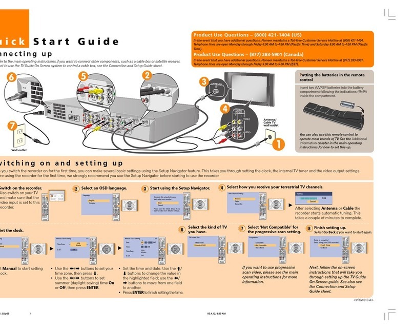
Pioneer PRV-LX1 Setup guide

PRV-LX1 DVD-Video Recorder
Field Training Guide
Technical Training Department
1925 E. Dominguez Street
Long Beach, CA 90810
Rev.1


Table Of Contents
Overall block diagram………………………………………..3~4
Block diagram overview……………………………………..5~6
Disassembly instructions……………………………………7~17
Service mode………………………………………………….18~21
Viewing log files……………………………………………....22~23
Status LED’s……………………………………………..…….24
Troubleshooting…………………………………………..…..25~28
Block diagram JKIB, JKDB, JKOB, HPVB & 422 IB…….29
Block diagram DECB assembly…………………………….30
Block diagram PCIB assembly………………………….…..31
Block diagram AVIB assembly……………………………...32~33
Block diagram PWRB, FLKB, DRV1B, DRV2B & USB…..34
Block diagram PWRB assembly………………………….…35
Upgrade Instructions………………………………………….36

!"
"
!
# "
$
$
"
%
$
$
&'$#
%
&'$#
%'
"#
"#
"#
%'
"#
%
"#
"#
%'
"#
"#
("
"
("
"
%'
"#
%'
)*
)*
)*
)%*
#
(
("
"#
(+
(+
('$
,'
%
)*
%''
$
"#
%
'
-
""-
""-
""-
.
%/
&'$#
01
!
""-
""-
""-
/
&'$#
'
&'$#
)%*
,'
%
)*
)*
,
,
-
,'
" "#
%%
'
"
'
)*
-"#
,"#
,
-
)*
)*
)*
,'
,
-
%
'
)*
'
"
234
%
356
%
%-
# "
# "
!$
7858
'
'-'0
+&
8589:
'')* '')* '')*
""""
)*
)*
,'
%-
.;
-
"
2 "
"
:<5
;
89=
)*
-
)'*
-
)*
-%
# "
"#
')"2*
)*
,
,
-
,'
)'*
# #
(>
"
"
'
!
8=85
"
"
"
(
$2
#
%
%!
%#
$2
)*
2"
"
"
)*
,'
,
-
"#
"#
)*
"
'
'
&% (
86
%
)*
?
%'
(2'
%'
(2'
%'
(2'
2+
2+
#
"
"
'
%
# "
"#
"#
$
2+
2
"
'
'$
'
?$
# "
"
0%
$
8589:
!$
%-%
( $
#
(
?$
86
# #
/
01
!
01
!
# "
?
#%%$
(>
% (2'
(2'
%
?
?
2+
2+
2+
'
)"2*
) *
?
!"
!"
!"
#
#
')"2*
!"
"
@%(>
!"#
$%$&
'((!) #
*+
,
*''-.
/,
$,
$
,
*
*
*
*
$
*
$0
*
$
*
1
23
2
2
2
1
4
2
5
6
6
26
26
2
,6
,6
,6
%
2
2
2
23
2
664
2
23
2
664
2
2
&
&
2
2
23
23
2
,6
,6
,6
161
$6
1
664
664
1614
2
7,&
,
7
,
,
1
,
1
,
2
%
&$
1
,
%
2
2
%
/
,
,/,
1
%
2
2
/
2
/
2
,* 1
2
2
2
2
&
$
&
$
&
,
8
8
%
8
8
%
1614
1
,6
,6
"( :)
Video Input
Audio Input
DV Input
Video Output
Audio Output
Video Driver & Switching IC
JKIB ASSY
1/3 AVIB ASSY
JKOB ASSY
HPVB ASSY
JKDB ASSY
AVIB ASSY
2/3
DECB ASSY
PCIB ASSY
3/3
2/2
1/3 DECB ASSY
PRV-LX1 DVD-Video Recorder
422IB ASSY
LTC IN
EXSYNC
FLASH
32M
3.

!"
"
!
# "
$
$
"
%
$
$
&'$#
%
&'$#
%'
"#
"#
"#
%'
"#
%
"#
"#
%'
"#
"#
("
"
("
"
%'
"#
%'
)*
)*
)*
)%*
#
(
("
"#
(+
(+
('$
,'
%
)*
%''
$
"#
%
'
-
""-
""-
""-
.
%/
&'$#
01
!
""-
""-
""-
/
&'$#
'
&'$#
)%*
,'
%
)*
)*
,
,
-
,'
" "#
%%
'
"
'
)*
-"#
,"#
,
-
)*
)*
)*
,'
,
-
%
'
)*
'
"
234
%
356
%
%-
# "
# "
!$
7858
'
'-'0
+&
8589:
'')* '')* '')*
""""
)*
)*
,'
%-
.;
-
"
2 "
"
:<5
;
89=
)*
-
)'*
-
)*
-%
# "
"#
')"2*
)*
,
,
-
,'
)'*
# #
(>
"
"
'
!
8=85
"
"
"
(
$2
#
%
%!
%#
$2
)*
2"
"
"
)*
,'
,
-
"#
"#
)*
"
'
'
&% (
86
%
)*
?
%'
(2'
%'
(2'
%'
(2'
2+
2+
#
"
"
'
%
# "
"#
"#
$
2+
2
"
'
'$
'
?$
# "
"
0%
$
8589:
!$
%-%
( $
#
(
?$
86
# #
/
01
!
01
!
# "
?
#%%$
(>
% (2'
(2'
%
?
?
2+
2+
2+
'
)"2*
) *
?
!"
!"
!"
#
#
')"2*
!"
"
@%(>
!"#
$%$&
'((!) #
*+
,
*''-.
/,
$,
$
,
*
*
*
*
$
*
$0
*
$
*
1
23
2
2
2
1
4
2
5
6
6
26
26
2
,6
,6
,6
%
2
2
2
23
2
664
2
23
2
664
2
2
&
&
2
2
23
23
2
,6
,6
,6
161
$6
1
664
664
1614
2
7,&
,
7
,
,
1
,
1
,
2
%
&$
1
,
%
2
2
%
/
,
,/,
1
%
2
2
/
2
/
2
,* 1
2
2
2
2
&
$
&
$
&
,
8
8
%
8
8
%
1614
1
,6
,6
"( :)
PC Mother Board
2/3
DECB ASSY
2/2 PWRB ASSY
1/2 PCIB ASSY
AVIB ASSY
1/3
DRV1B
ASSY
DRV2B
ASSY
KEYB
ASSY
FLKB
ASSY
PWRB
ASSY
1/2
2/2 ATX
POWER
1/2
ATX POWER
USBB ASSY
Overall Block Diagram
120GB HDD
DRIVE 1
DRIVE 2 (OPTION)
MASTER
SLAVE
MASTER
IDE 1
IDE 2
UPS
VGA
ETHERNET (15P)
REAR USB (4Px2)
COM 2
FAN (DRV2)
FAN (DRV1)
FAN (REAR
DVI OUTPUT
FRONT USB
(4Px2)
FLASH
32M
PCI SLOT 2
PCI SLOT 3
RS422
Control
4.

Block Diagram Overview
(JKIB Assembly)
All inputs Video and Audio (Composite, Component Beta or SMPTE,
S-Video, DV, Balanced and Unbalanced Audio) enter and pass
though the JKIB assembly and enter the AVIB assembly. If using the
composite input in through mode the unprocessed audio and video
pass back directly to the JKOB output assembly for monitor viewing.
(AVIB)
Video and Audio signals entering the AVIB assembly are subject to
analog to digital conversion, time based correction and digital noise
reduction will be added if selected by the user. On this assembly the
signals next are MPEG encoded and sent out to the PCIB assembly.
(PCIB)
The two main functions of the PCIB assembly are.
1. RS422 control interface.
2. PCI interface for the MPEG encoded signals.
Output signals from this board enter the PC Mother board (PCI slot 3)
(DECB)
The DECB assembly receives its input from the PC Mother board
(PCI slot 2) into its PCI interface conversion IC. After conversion back
to a MPEG stream the signals pass through the MPEG decoder and
digital to analog converters for both audio and video. At this point the
analog video and audio output to the JKIB assembly.
(JKOB)
The JKOB or jack panel output board receives input audio and video
signals from the JKIB assembly. In turn it outputs directly to the back
panel.
5.

Block Diagram Overview
(PC Mother Board)
The main circuit board assembly in this device is a very high quality
Pentium based personal computer main board. It interfaces directly
with the front panel control by an RS232 connection on COM 2. In
addition it has front and rear USB ports, a RS232 connection for a
UPS, 3 PCI slots (2 used), an Ethernet connection and VGA output.
Main system processor (Intel Celeron 2 GHz) with 256 Mb ram.
(ATX Power)
The ATX power assembly is similar to a home or office PC supply. It
provides +12, -12, +5, -5 and +3.3 voltage supplies to the PWRB
assembly.
(PWRB)
This main power supply assembly provides DC supply to all circuit
boards and drives 3 of the 5 fans used in this product.
(JKDB)
This assembly contains the RS422 interface and output RS422
connector. It also interfaces the external sync input to the DECB
board and the LTC (linear time code) to the PCIB board.
(422IB)
The RS422 input connector assembly provides input to the 422 driver
IC located on the JKDB board.
(HPVB)
Headphone output volume and driver assembly. Located on the front
panel.
(FLKB)
Front panel assembly. This board includes the florescent display
driver and IR remote control decoder. This board along with its main
CPU communicate directly to the PC motherboard through the RS232
Com 2 port.
6.

PRV-LX1 Disassembly
1. Top cover and side panels
1. Remove seven screws and lift off the top cover.
2. Remove eight screws for the L and R side covers.
2. Front Panel
1. Remove the front volume knob.
2. Remove the Filter covers and Air filters.
3. Remove two screws.
4. Remove three screws
5. Remove Front Panel Unit.
7.

Front & Rear Bridges must be removed in order to access drives and board
assemblies.
1. Remove 12 screws for the front & 8 screws for the rear bridge.
2. Remove bridges.
8.

3. Drive Assy LX1
1. Disconnect two connectors.
2. Remove four screws and DVDR Drive Assembly.
9
9.

4. HDD Assy
1. Disconnect two connectors.
2. Remove four screws.
A
ttention: One screw is under the label.
3. Pull up on the handle and remove HDD Assy.
10.

5. AVIB Assy
1. Remove four screws.
2. Remove Rear bridge.
3. Disconnect four FFC cables and four connectors.
4. Remove four screws.
5. Remove AVIB Assy with AVI shield and base.
11.

6. JKIB Assy & JKOB Assy
1. Disconnect two FFC cables and a connector.
2. Remove nine screws (JKIB Assy).
3. Remove nine screws (JKOB Assy).
4. Remove three screws.
5. Remove JKIB Assy with PCI cover and Jack stay.
X
6. Remove JKOBAssy.
12.

7. DECB Assy & PCIB Assy
1. Disconnect two connectors.
2. Remove two screws of Rear Panel.
3. Remove two screws.
4. Pull up DECB Assy from PCI slot of Mother Board.
5. Pull up PCIB Assy from PCI slot.
6. Remove two screws, 4P Power connector and Flat cable clamp.
13.

8. PWRB Assy
1. Remove Center stay and Front Bridge with 12 screws.
2. Disconnect eight connectors.
3. Remove three screws.
4. Remove the hook of Card edge spacer.
5. Remove PWRB Assy.
14.

9. MOTHER BOARD Assy
1. Disconnect two connectors.
2. Remove seven screws.
3. Remove MOTHER BOARD Assy
10. ATX Power Supply Unit
1. Remove one screw inside.
2. Remove four screws outside.
3. Remove ATX Power Supply Unit.
15.

11. Exchange the FAN of Power Supply
1. Remove a screw and move switch barrier.
1. screw Switch barrier
2. Remove Fan cover and disconnect a connector.
Fan connector
3. Exchange the FAN.
4. Connect FAN connector.
5. Install Fan cover.
6. Move switch barrier and secure a screw.
16.

*Cable Styling of Power Supply
17.

Service Mode
Test mode Function List Using Service Remote Control (GGF1067 or GGF1381)
Input Remote Control Code Function memo
[ESC]+[TEST] Test Mode
[CX] FAN Test Mode
[0] All FAN ON
[1] All FAN OFF
[2] Left FAN ON
[3] Left FAN OFF
[4] Right FAN ON
[5] Right FAN OFF
[6] Rear FAN ON
[7] Rear FAN OFF
[9] Exit
[P.RUN] LED/FL Test Mode
[0] Exit
[1] Turn on all FL/LED light
[2] Turn off all FL/LED light
[TV/LDP] Front Panel switch Test Mode *1
[0] Exit
[STEREO]+[8] Region number of Drive1 on display
[STEREO]+[9] Region number of Drive2 on display
[REP.A] System Information on display *2
[0] Exit
[1] Main System on display
[2] USB Interface on display
[3] Network Interface on display
[4] Primary Master Drive on display
[5] Primary Slave Drive on display
[6] Secondary Master Drive on display
[7] Secondary Slave Drive on display connected Drive2
[8] Error History of Drive1 on display
[9] Error History of Drive2 on display connected Drive2
[REP.B] Loop back Test Mode
[0] Exit
[1] RS-422A Loop Back Test
[2] RS-232C Loop Back Test
[3] RS-422A Loop Back Test (Error Stop)
[4] RS-232C Loop Back Test (Error Stop)
[A.MON] Power On Time Clear
[0] HDD Access Time
[1] Power On Time of PRV-LX1
[8] Copy the setting file for using FTP(Network)
[9] Copy the log file for using FTP(Network)
18.
Caution! This will clear the timer

Service Mode
Input Remote Control Code Function memo
[ESC]+[TEST] Test Mode
[PLAY] Measuring Error Rate
[SCAN F] +0x10000
[SCAN R] -0x10000
[1] Start measuring of Drive1
[2] Start measuring of Drive2
▲/■Stop measuring
[ESC]+[TEST] [0] RS-422A and 232C Interface Test Auto start [1]-[4]
[1] RS-422A Loop Back Test
[2] RS-232C Loop Back Test
[3] LAN Test
[4] USB Test
[5] Measuring Error Rate of Drive1 *3
[6] Measuring Error Rate of Drive2
[7] LTC on FL
[CLEAR] Clear on display
[ESC] Escape Test Mode
[ESC]+[DISP] Debug Mode *4
[DISP] Enter next page
---Page1--- : PRV-LX1 Information
---Page2--- : DVD Play Information
---Page3--- : Decode Information of DECB Assy
---Page4--- : Encode Information of PCIB Assy and AVIB Assy
---Page5--- : Encode Information of Application
---Page6--- : Linux information
*1: Test mode of front panel button input
When you enter this mode all segments on the FLdisplaylight up. Pressing front panel keyswill turn off segments
one byone.
After the all keys have been pushed, only 3 blocks remain on. (only 2 blocks-> with 2 drives)
*2: System Information on display
[1]: Main System
-CPU --- Confirmation of the CPU clock
-Memory --- Confirmation of the capacity of memories
-User Data --- Confirmation of the free space of the HDD (User Area)
-PCI --- Confirmation of the PCI boards was recognized from Linux OS
[2]: USB
- Connected USB products on display. (keyboard & mouse)
[3]: Network
-IP Address/Network/MAC Address
19.
Open or close drive trays
(ESC)+(front panel buttons or remote control
Other manuals for PRV-LX1
15
Table of contents
Other Pioneer DVR manuals

Pioneer
Pioneer DVR-231-S User manual

Pioneer
Pioneer DRM-7000 Manual

Pioneer
Pioneer DVR-543H-S User manual

Pioneer
Pioneer Recorder Instruction Manual

Pioneer
Pioneer DVR-231-S User manual

Pioneer
Pioneer DVR531H User manual

Pioneer
Pioneer DVR-LX61D User manual

Pioneer
Pioneer HTZ-929DVR User manual

Pioneer
Pioneer dvr-3100-s User manual

Pioneer
Pioneer DVR-810 H Quick start guide