Raymarine Ray54 User manual

Page: 1 of 8
THEORY OF OPERATION
Ray54/E For Raymarine
2004 Feb 27
This PLL controlled VHF marine mobile transceiver provides an accurate and stable multi-channel
operation.
The transceiver consists of 13 main sections
!" Transmitting stage
!" Receiving stage
!" Local oscillator PLL (Phase Lock Loop) Circuit
!" Memory backup
!" Low voltage detection
!" Large LCD
!" Local/distance Circuit
!" 2nd Receiver
!" WX Alert Circuit (only USA)
!" PC Program
!" DSC Feature
!" GPS Message
!" ATIS Feature (only EU)
!" Transmitter Stage
The audio is picked up from the internal Mic. The audio signal is then amplified by Audio Amplifier, IC205C ,
IC205B and filtered by a low pass filter IC10C, IC10D. The audio that is adjusted by VR3 to obtain a
suitable RF frequency-deviation, modulates the carrier of VCO, through Varicap (VD302).
The modulated signal output from the VCO is pre-amplified by Q2, and IC1 . When the supply voltage is
13.6V, this signal will be amplified up to 1W or 25W. The signal is filtered by low-pass filter circuit of which
consists of L1, L2, L4, C1, C2, C3, C5, C6, C14, C47 and C62.These low pass filters are necessary to
suppress the second and the third harmonics as higher. The signal is then fed into the antenna input and
radiated out. The signal is also fed into another path consisting of C9, C10, D3, D4 for sampling, and is
converted into a direct current voltage for the Automatic Power Control (APC) circuit IC12, Q5, Q14, Q15,
Q24 to control the voltage of IC1 Pin 2 to maintain the output power stability. Q15 is used control Hi/Lo
power
When the unit is transmitting, the channel control voltage is added to the TX VCO varicap VD306. The
capacitance of VD302 is varied following the audio signal, therefore the carrier is modulated to form the
modulated signal.

Page: 2 of 8
!" Receiver Stage
The receiver uses a double frequency super-heterodyne circuit. The first Immediate Frequency (IF) is 21.4
MHz and the second is 450 kHz.
The RF signal is received by the antenna, and passes through a low-pass filter network L1, L2, L3, L9, C1,
C2, C3, C5, C6, C14, C47 and C62 to filter out unwanted signal. The received RF signal then passes
through a high RF transformer L10 and is amplified by RF amplifier Q9. L11, L12, L13, C15, C18, C20
form the band pass filter. The RF signal then is mixed with the local oscillation frequency by the mixer D22,
D23. The first IF (Immediate Frequency) 21.4 MHz is produced. This IF is passed through a coil T2 and a
pair of crystal filter F1, F2 to further filter out other unwanted signals. The first IF then is amplified by Q11
and the IF amplifier IC7. (IC7 is an integrated IF amplifier which consists of a local oscillator, a
demodulator, a second mixer, squelch control circuit, and IF amplifier). The 21.4 MHz IF then is mixed here
with second mixer and converted into 2nd Immediate Frequency (IF) 450 kHz. The 2nd IF passes through
a ceramic filter F4 to filter out the residue unwanted signal at pin 5 of IC7 output this final IF signal and The
demodulated AF signal is output at pin 9 of IC7.
The demodulated AF signal pass through IC15 then passes through a volume control VR201 through
de-emphasis circuit feeding IC10A, IC10B.and finally amplified by Audio amplifier IC11 and heard in the
speaker.
The squelch control signal also produced by IC7, the rectified noise signal is output by Pin 14 of the IC7.
Pass through the network by composition of C170, R44 are sends the digital squelch control signal to the
MCU to mute the audio speaker path and to indicate the RX station on LCD, R214, R217 and VR203 form
a variable resistor, which correspond to the squelch level.
!" Local oscillator PLL (Phase Lock Loop) Circuit:
The receiver and transmitter both share the same PLL (Phase Lock Loop) Circuitry to produce the carrier
frequency or the receiver local oscillation frequency. The local oscillator consists of a fundamental
frequency oscillator Q301 and A phase Lock Loop (PLL) IC16 When Rx 5Vvoltage is supply, the VCO will
produce receiver local oscillator frequency. The high stability frequency is determined by crystal X2
(20.950 MHz) and as the PLL reference oscillator. This signal is frequency-divided by IC16 and a 12.5 kHz
signal is produced. When the VCO frequency applied to IC16 pin1 and frequency-divided by IC2 produces
a frequency comparable to 12.5 kHz, PLL IC pin 3 will output a PD voltage to control the VCO. When
these two frequencies are matched, a constant control voltage is output from PLL to lock VCO in desired
frequency. Otherwise the PLL IC pin 5 will also output a unlock indication to MCU to indicate that the PLL
is in the frequency unlock state.
Page: 3 of 8
!" Memory Backup
IC201 is an EEPROM AT24C64, which acts as a memory backup for the working channel code and the
system parameters. Every time when the unit is switched on, the MCU will reset the system, clear the
RAM, and recall the memory from the EEPROM to refresh the RAM in MCU IC203.
!" Low Voltage Detection
The battery voltage divided byR250 and R251 through R254 is input to IC203 for voltage level detection. If
the battery voltage drops below 9.5 V, LCD will indicate the battery is in low state.
!" Large LCD
All message through series bus from MCU to display driver IC401 and will be displayed through a
34×52mm 4×12 characters dot matrix LCD display.
!" Local/distance circuit
Local/distance circuits are composed of Q16, R195 and R88. When local SW is on high level, receiver
sensitive is high otherwise is on low.
!" 2nd Receiver
2nd receiver circuit is as figure. RF input is from C101 of main PCB, the received RF signal then passes
through a high RF transformer L505 and is amplified by RF amplifier Q501, L506, L507, L508, C15, C18,
C20 form the band pass filter. Then passes through a high RF transformer L509 is mixed with the first local
oscillation frequency by the mixer D501, D502, D503, D504. The first IF (Immediate Frequency) 17.9 MHz
is produced. This IF signal is passed through a transformer coil L510 and a pair of crystal filter F1, F2 to
further filter. The first IF then is amplified by Q503 and the IF amplifier IC501. IC501 is an integrated IF
amplifier which consists of a 2nd local oscillator (18.355Mhz),a demodulator, a second mixer, squelch
control circuit, and IF amplifier circuits). The 17.9MHz IF then is mixed here with second mixer and
converted into 2nd Immediate Frequency (IF) 455 kHz. The 2nd IF passes through a ceramic filter F503 to
filter out the residue unwanted signal at pin 5 of IC501 output this final IF signal and The demodulated FSK
signal is output at pin 9 of IC501 through R517 C543 pass J501.J4 fed in IC15 pin 13 of the main PCB.
The squelch control is also controlled by IC501. The audio signal passes through the low pass filter R514,
R515, C541 and IC501 internal squelch control R516, and C542 that form as a squelch amplifier to
produce a squelch signal (noise) from pin11 of IC501 output, this signal is then amplified by Q505 and
regulated by D505 to produce a direct current voltage as a control voltage then it is fed throughR526and
pin14 to IC501 from pin13 output the busy signal.
!" WX Alert Circuit (only USA)
The 1050Hz tone of receiver through IC6A composed band-pass filter and IC6B amplifier form square

Page: 4 of 8
wave signal. To fed IC203 pin 97produce weather alert.
!" PC Program
J203 on CPU is connected with the outside cabinet through a cable with a round pin8 plug. Software
upgrade and clone can be functioned when an exclusive interface control box is connected with RS-232
interface of computer.
When the light on control box is green, J203 pin3 is high level (5v), CPU programming is performed, and
the software is upgraded. When the light on control box is red, clone function is performed.
!" DSC Feature
!" DSC TX Encoded by MCU IC203, through RP1, R237, R234, produces D/A convert, and IC205D low pass
filter forms FSK signal. This signal is amplified by IC205A and filtered by IC10C, IC10D to modulate VCO
frequency from the DSC signal transmit output.
DSC RX decode: DSC signal from 2nd receiver is Send to IC15 pin13 on the main from pin 14 of IC15
output, then the signal passes through IC6C high-pass filter and IC6D low-pass filter form FSK signal. This
FSK is signal decoded by IC609. The DSC is restored by IC203 [MCU] with RX data from pin1 Of IC609
!" GPS Message
External GPS Message is input to MCU through phototransistor IC207 LCD will display the machine
current location and time message in idle state.
!" ATIS Feature (only EU)
ATIS encoded by MCU (IC203), through RP1, R237, R234, produces D/A conversion, and IC205D low
pass filter forms FSK signal. Through the attenuation be composed of R215, R218, R274 and Q204 This
signal is amplified by IC205A and filtered by IC10C, IC10D to modulate VCO frequency forming the ATIS
signal transmit output.
ATIS signal is received and demodulated by IC7. Demodulated signal is sent into pin12 of IC15, from pin
14 of IC15 output .the signal passes through IC6C high-pass filter and IC6D low-pass filter to get ATIS
FSK signal and filter out residual unwanted signals. This FSK is signal decoded by IC609. The ATIS is
restored and processed by MCU IC203 with RX data from pin1 of IC609. Be formed control signal to
production about 100ms squelch to mute audio speak path.

Page: 5 of 8
ALIGNMENT PROCDDURES
This transceiver is completely aligned at the factory and does not require any adjustments for installation.
However it is considered as good practice to verify that none of the adjustments are changed.
Do not adjust any circuitry in this radiotelephone unless you understand the circuit operation and have
experience in adjusting radiotelephone. Tampering with the radiotelephone may upset the alignment and
lower its performance.
Test Equipment Required:
!" Regulated DC power supply, 10 -16V adjustable, 7A
!" Audio signal generator, 10Hz~3kHz
!" Digital multimeter
!" Deviation meter {linear detector}
!" Frequency counter, 0~500MHz high impedance
!" Oscilloscope
!" RF power meter, ≥30W
!" High frequency standard generator, >500MHz
!" Tracking generator, >500MHz
!" Distortion analyzer
!" Audio level meter
!" T-coupler
!" Sinad meter
!" Alignment drivers, etc.
!" Or a radio communication test set 2955 (MARCONI INSTRUMENTS)

Page: 6 of 8
ADJUSTMENT PROCEDURE
Step Item Adjustment Procedure
1, PLL L302, L307 RX PD voltage=1.6V TX PD voltage =2V, at CH16
2 TX Frequency VC2 Adjust VC2 to obtain demanded TX frequency. ±200Hz
3 TX Power Hi VR5 Adjust VR5 to obtain demanded TX power 23±2W.
4 TX Power Low VR6 Adjust VR6 to obtain demanded TX power 0.8±0.1W
5 TX Deviation VR3 1. Inject an audio frequency (AF) –20dBm.
2. Adjust VR3 to obtain maximum TX deviation ≤5kHz.
3. Check MIC modulation sensitivity, which should be
2.5~10 mV
6 RX Sensitivity L10, L11, L12,
L13, L14, L19,
T1, T2, T3
1. Check RX sensitivity if it is normal.
2. Adjust L10, L11, L12, and L13 to obtain Best Frequency
response.
3. Adjust T1, T2 to obtain Best Frequency response.
4. Adjust L14, L19 to obtain Best sensitivity.
5. Adjust T3 to obtain Best SIAND AND Distortion. When at
antenna terminal input 1mV RF signal and modulated with
normal test modulation.
6. Repeat step 1 to 5.at CH28 and CH3.
7 DSC test Check Modulation index for DSC. Modulation index for DSC.
Frequency error (demodulated DSC signal)
8 ATIS test Check Modulation index for ATIS. Modulation index for ATIS.
Frequency error (demodulated ATIS signal)

Page: 7 of 8
TROUBLESHOOTING
Before troubleshooting, prepare your unit as follows:
!" Connect the power supply.
!" Turn volume control fully clockwise so that it is all the way up.
Item Symptom Cause/Remedy
1 Unit is not able to turn on. !" Check the power voltage and power switch.
!" Check to see if regulator IC8 defective.
2 No sound with AF signal
applied to pin 6 of IC6.
!" Check to see if IC1 and /or associated components is
Defective.
!" Check to see if speaker on control circuit VR201, IC10A,
IC10B, is defective.
3 Squelch circuit inoperative. !" Check to see if VR203 is defective.
!" Check to see if IC4 is defective.
4 No receiver (RX) !" Check to see if IC11 is defective.
!" Check to see if IC7 audio output at pin 9 is defective.
!" Check Q12.
!" Check 21.4MHz output of first mixer Q10.
!" Check 21.4MHz output of crystal filters F1, F2.
!" Check 21.4MHz output of first IF amplifier Q11.
!" Check 450kHz signal from ceramic filter F3.
!" Check to see if VCO circuit is defective.
!" Check to see MCU is defective.
5 Low receiver sensitivity !" Check to see if antenna is bad connecting.
!" Check to see if the output from Q9, Q10, Q11 and F1 F2 is
defective.
6 No transmission (TX) !" Check to see if the PTT switch is defective.
!" Check to see if Q13 is defective.
!" Check to see if power transmit circuit Q1, Q2, Q3 are
defective.
!" Check to see if VCO circuit is defective.
!" Check PLL control voltage if it reads 2±0.2V at 156.05MHz.
7 Poor or no modulation !" Check to see if the microphone or MIC jack is defective.
!" Check to see if IC205 and/or its associated components are
defective.
8 Deviation of transmit frequency !" Check the frequency of 20.950MHz crystal X2.
!" Adjust VC2 and verify the transmit frequency.

Page: 8 of 8
DISASSEMBLY INSTRUCTIONS
To disassembly follow the procedures below:
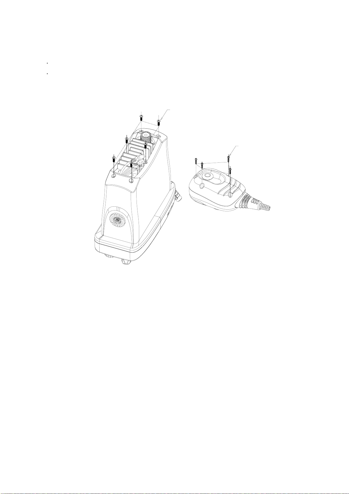
AUnscrew the 4Screws of hand MIC.
BUnscrew 6 screws for the bottom cabinet of the main UNIT.
A
B
Other manuals for Ray54
1
This manual suits for next models
1
Table of contents
Other Raymarine Transceiver manuals

Raymarine
Raymarine Ray 53 Installation instructions

Raymarine
Raymarine AIS500 User manual

Raymarine
Raymarine Ray101 User guide

Raymarine
Raymarine AIS350 User manual

Raymarine
Raymarine AIS700 User manual

Raymarine
Raymarine AIS500 User manual

Raymarine
Raymarine AIS700 User manual

Raymarine
Raymarine AIS950 User manual

Raymarine
Raymarine AIS700 User manual

Raymarine
Raymarine AIS700 User manual