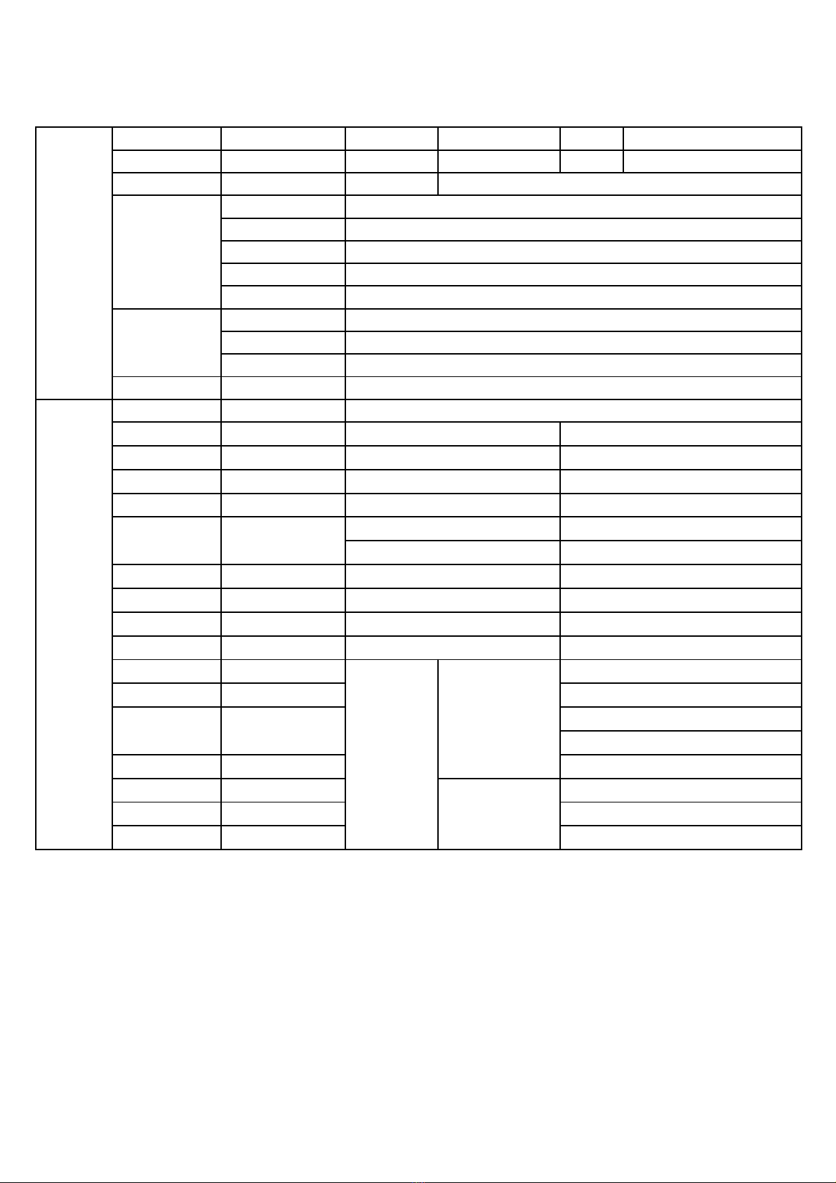
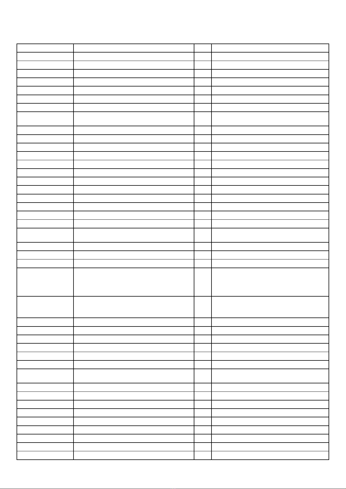
ITEM SPEC. QTY LOCATION
19-AB0222-JTX RES SMD 2.2K OHM 1/10W 0603 2 R147;R146
19-AB0223-JTX SMD. RES 22K OHM 1/10W +/-5% 0603 21 R061;R053;R052;R051;R050;R049;R225;R047;
R226;R046;R222;R223;R054;R048;R060;R031;
R059;R058;R057;R056;R055
19-AB0243-JTX SMD. RES 24K OHM 1/10W +/-5% 0603 1 R137
19-AB0271-JTX SMD. RES 270 OHM 1/10W +/-5% 0603 1 R217
19-AB0332-JTX SMD RES 3.3K OHM 1/10W 0603 6 R122;R131;R140;R150;R168;R171
19-AB0392-JTX SMD. RES 3.9K OHM 1/10W +/-5% 5 R135;R136;R219;R220;R036
19-AB0470-JTX RES SMD 47 OHM 1/10W +/-5%0603 20 R099;R075;R081;R134;R154;R126;R133;R085;
R087;R123;R124;R151;R139;R138;R121;R120;
R119;R118;R083;R117
19-AB0472-JTX RES SMD 4.7K OHM 1/10W 0603 10 R115;R144;R145;R224;R006;R007;R008;R029;
R033;R093
19-AB0473-JTX SMD. RES 47K OHM 1/10W 0603 7 R041;R026;R045;R044;R040;R042;R043
19-AB0682-JTX RES SMD 6.8K OHM 1/10W 0603 1 R025
19-AB0750-JTX SMD. RES 75 OHM 1/10W 0603 13 R011;R190;R187;R173;R170;R169;R157;R156;
R155;R002;R005;C195;R014
19-CD0000-JTX RES.SMD 0 OHM 1206 4 L029;L027;L025;R022
23-A08220-JBX NETWORK RES. 22 OHM +/-5% 16 RP017;RP023;RP022;RP021;RP024;RP025;
RP019;RP031;RP020;RP032;RP018;RP030;
RP029;RP028;RP027;RP026
23-A08470-JBX CHIP ARRAY RES. 47 OHM +/-5% 0603*4 24
RP035;RP037;RP047;RP046;RP045;RP044;
RP043;RP042;RP041;RP040;RP039;RP038;
RP034;RP033;RP011;RP006;RP007;RP009;
RP036;RP005;RP004;RP003;RP002;RP001
28-AB0102-JCX SMD. CAP 1000PF 50V +/-5% 0603 5 C215;C164;C191;C184;C176
28-AB0103-ZFX CAP.SMD 10NF 50V +80-20% 0603 2 C019;C018
28-AB0104-ZFX CAP. SMD 0.1UF 50V +80%~-20% F 1 C216
28-AB0120-JCX SMD. CAP 12 PF 50VDC 0603 +/-5% 3 C180;C179;C178
28-AB0180-JCX SMD. CAP 18 PF 50V +/-5% 0603 8 C158;C202;C201;C083;C084;C085;C200;C157
28-AB0224-ZFX CAP.SMD 0.22UF 50V +80-20%0603 6 C173;C174;C177;C187;C192;C196
28-AB0392-KBX SMD. CAP 3900 PF 50VDC +/-10% 0603 1 C159
28-AB0393-ZFX SMD. CAP 0.039 UF 50V +80%-20% 1 C160
28-AB0471-JCX CAP.SMD 470PF 50V +/-5% 0603 1 C214
28-AC0105-ZFX SMD. CAP 1 UF 16VDC +80%/-20% 2 C213;C217
28-AD0104-ZFX SMD CAP 0.1UF 25V +80-20% 0603 128
C062;C063;C065;C064;C080;C082;C077;C168;
C166;C073;C074;C075;C109;C105;C091;C104;
C076;C066;C079;C078;C172;C054;C055;C056;
C057;C058;C059;C060;C061;C087;C088;C089;
C090;C096;C170;C167;C169;C053;C086;C098;
C099;C100;C101;C102;C072;C068;C069;C070;
C071;C095;C114;C118;C119;C097;C081;C013;
C023;C024;C014;C001;C015;C016;C103;C092;
C093;C094;C130;C129;C128;C127;C126;C125;
C124;C123;C122;C121;C133;C148;C067;C171;
C120;C131;C163;C156;C155;C154;C151;C150;
C183;C186;C185;C175;C149;C132;C181;C182;
C165;C051;C052;C025;C005;C006;C007;C147;
C032;C134;C021;C136;C137;C138;C139;C140;
C022;C046;C048;C050;C008;C146;C145;C144;
C141;C031;C030;C029;C028;C027;C026;C002
28-RA0107-MAX SMD. CAP 100 UF 10V +/-20% 6 C115;C111;C110;C135;C152;C116
28-RC0106-MAX SMD. CAP 10 UF 16V +/-20% 13 C039;C040;C038;C017;C020;C045;C044;C043;
C041;C042;C037;C036;C035
28-RC0226-MAX SMD. CAP 22 UF 16V +/-20% 2 C033;C034