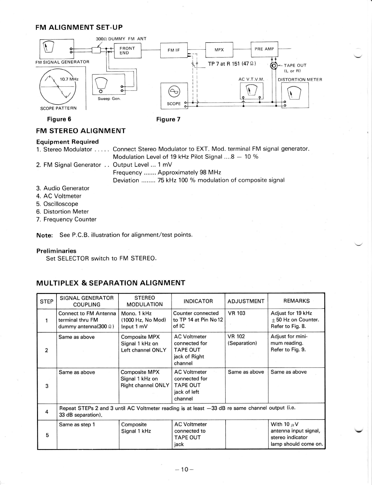
Realistic STA-21 User manual

STA.21
AM /FM STEREO RECETVER
Catalog Number : 31 -2071
cusT0M MANUFACTURED FOR RAD|0 SHACK [ln DMS|0N 0F TANDY C0RP0RAT|0N
J

(1} ELECTRICAL PERFORMANCE SPECIFICATIONS ..... 3 -
(2} DISASSEMBLY INSTRUCTIONS .
(3) BLOCK DIAGRAM
(4) ALIGNMENT INSTRUCTIONS .,. 7 -
(5) TROUBLE SHOOTING . . , 12 -
(6) DIAL STRINGING DIAGRAM
(7) IC & TRANSISTOR LEAD IDENTIFICATION .
(8) AM/FM TUNER, IF & MPX ASSEMBLED BOARD
(TOP & BOTTOM VIEWS)
(9) PRE & TONE AMP ASSEMBLED BOARD
(TOP & BOTTOM VIEWS)
(10) MAIN AMP & POWER SUPPLY ASSEMBLED BOARD
(TOP & BOTTOM V|EWS) ....... 18
(11) JACK ASSEMBLED BOARD
(TOP & BOTTOM VTEWS) ....... 19
(12) ELECTRICAL PARTS LIST . , . ,. 19 - 27
(13) EXPLODED VIEW PARTS LIST . 28 - 30
(14) IC INTERNAL DIAGRAM ...... 31
(15) SCHEMATIC DIAGRAM . 32 - 33
(16) EXPLODED VIEW 34 - 35
4
5
b
11
14
15
15
16
17
-2-

1. ELECTRICAL PERFORMANCE SPECIFICATIONS
AM BAND
Range
IF
Antenna Sensitivity for S/N 20 dB
at 600 kHz
at 1000 kHz
at 1400 kHz
Terminal Sensitivity (20 dB S/N)
ACA at S/N 6 dB sensitivity at 1000 kHz
AGC Distortion at 1000 kHz, 100 mV/m, 80% Mod.
AGC Figure of Merit
lF Rejection at 600 kHz
lmage Rejection at 1400 kHz
Distortion at 5 mV/m 30% Mod.
Tapeout Level at 5 mV/m 30o/o Mod. 400 Hz
Fidelity 5 mV/m lnput, -6 dB Down (1 kHz:0 dB)
Whistle Modulation of 2nd and 3rd Harmonic
atland5mV/m
Calibration Accuracy at 600 kHz
at 1400 kHz
FM BAND
Range (For UL and C.S.A. Models)
Range (For European and Australian Models)
IF
IHF Sensitivity at 90, 98 and 106 MHz
FM S/N Ratio at 98 MHz, 1 mV lnput
FM Limiting -3 dB
lF Rejection at 90 MHz
lmage Rejection at 106 MHz
Capture Ratio
ACA + 400 kHz at 100 pV
Audio THD 400 H2,75 kHz Dev.
Audio THD 400 H2,22.5 kHz Dev.
Calibration Accuracy at 90 MHz
at 106 MHz
AFC Holding Range with 1 mV Signal
AM Suppression
Maximum Signal Handling Capacity
Tapeout Level 1 mV 75 kHz Dev. 400 Hz Mod.
All Sets must meet the Requirements of the FCC.
UNIT
(kHz)
(kHz)
I pV /ml
( zV)
(dB)
(o/ol
(dB)
(dB)
(dB)
l'/ol
(mV)
(Hz) 50
(o/ol
(kHz)
(kHz)
UNIT
(MHz)
(l.VlHz)
(MHz)
( pYl
(dB)
( pV)
(dB)
(dB)
(dB)
(dB)
lo/ol
(o/ol
(kHz)
(kHz)
(kHz)
(dB)
(v)
(mV)
NOM INAL
510 - 1650
455
200
200
200
10
28
4
45
32
45
1.5
250
- 2500
LIMIT
520 - 1620
500
500
s00
NOMINAL LIMIT
86.5 - 108.5 88 - 108
87.5 - 108.5 87.5 - 108
10.7
2.8
60
3.2
80
50
3
45
0.5
0.3
+ 200
38
0.2
750
20
10
38
27
35
3.5
200
10
t25
+50
;:;
55
7.1
70
45
6
30
1.0
0.8
t 500
+ 500
300 - 800
30
0.1
750 + 2.5 dB
:
Frequency Response must meet the 75 1-usec.De-emphasis for UL and C.S.A. Approved Models
(50 p sec.De-emphasis for European and Australian Models).
-3-

FM MPX
Stereo lndicator "ON" Point
Separation at 1 mV 100 Hz
1 kHz
10 kHz
Stereo Distortion 1 mV 1 kHz
38 kHz Rejection
SCA Rejection
AUDIO SECTION
lnput lmpedance PHONO MAG.
AUX
Output Power at THD 1% 8 ohms
Both Channels Driven at 1 kHz
Power Bandwi<ith B ohrns Both Channels Driven
TH D 1 o/o, 20 Hz - 20 kHz
Sensitivity for Rated Power
PHONO MAG.
AUX
Tape ln
Frequency Response at AUX (1 W t 2 dB)
Bass Action at 100 Hz
Treble Action at 10 kHz
Min. Volume Hum and Noise
Max. Volume Hum and Noise Tone Max. at AUX
Signal to Noise Ratio
PHONO MAG. 5 mV Input (lnput Short)
AUX 200 mV lnput
Cross Talk at 1 kHz AUX
Bass Compensation at 100 Hz -30 dB Volurne
Treble Compensation at 10 kHz -30 dB Volume
Tapeout Level PHONO MAG. at 3 mV 1 kHz
AUX at 200 mV 1 kHz
PHONO MAG. Eq. Response at 100 Hz
at 10 kHz
Tapeout Level (DlN Connector)
AM 5 mV,/m lnput 30% Mod.
FM 1 mV lnput 22.5 kHz Dev.
AUX 200 mV lnput
PHONO MAG. Overload
NOTE:
UNIT
( ,,rV)
(dB)
(dB)
(dB)
lo/ol
(dB)
(dB)
UNIT
(K ohm)
(K ohm)
(w)
(w)
(mV)
(mV)
(mV)
(Hz) 15
(dB)
(dB)
(mV)
(mV)
(dB)
(dB)
(dB)
(dB)
(dB)
(mV)
(mV)
(dB)
(dB)
(mV)
(mV)
(mV)
(mV)
NOMINAL
10
29
34
26
0.6
42
42
LIMIT
20
?2
27
20
2.0
35
35
NOMINAL
50
100
11
8.5
2.5
150
't50
-30K
+10
+10
1
15
60
65
46
+9
+4
200
200
+13
-13
LIMIT
8.5
25
25
25
80
7
3.5
200
200
20-20K
t 10 t2.5
t 10 +2.5
3
70
55
55
40
+9 +2
+4 X2
200 + 2dB
200 + 2dB
+13 +2
-13 +2
25 + 3dB
25 + 3dB
25 t 3dB
60
The supply voltage is 120 volt AC (for UL and C.S.A. Models) (use 220/240 volt AC for European
and Australian Models), from a regulated power supply. The Power Source must insulated from
other equipment connected to antenna or output. The room temperature is 25 degrees C.
Nominal Specs represent the design specs; all units should be able to approximate these - some
will exceed and some may drop slightly below these specs.
Limit Specs represent the absolute worst condition which still might be considered acceptable; in
no case should a unit perform to less than within any Limit Specs.
-4-

2. DISASSEM BLY I NSTR UCTIONS
1)To remove chassis from wooden
cabinet.
Turn the cabinet upside down and
remove the five Pan head screws from
the cabinet bottom.
2) Removal of front panel (Aluminum
panel )
a) Remove the chassis from wooden
cabinet as described in 1).
b) Pull out the main chassis.
c) Remove the two Pan head screws from
the top and the three Pan head screws
from the bottom of the front panel.
d) Remove knobs and pull off panel.
3) To remove rear panel from chassis.
Remove the four Pan head screws from
the rear panel.
-5

3. BLOCK DIAGRAM
;P L
;; =i
aa >E
oo Io
";
o
o
o
d
o
d
o
$
o
";o
r
2
z
>z
z
z
Zz F
z-
O-O
6"HH
d<FF
t_l
;l
il,
ftN
a>o
OF
>E
)z
!d
1A
OI
ri
OF
-z
zo
ou
>= !2o
rH
>r
>l
=
E
o
L=
E
u
=
o
2
2t
]U
FF
=
!2
?"3
uF"
":5
=*L
o9
_c
-6-

4. ALIGNMENT INSTRUCTIONS
MAIN AMPLIFIER AND RESET CIRCUIT ADJUSTMENT/CHECK
NOTE o Maintain line voltage at 120 volts. (UL, C.S.A.) (Use 220/240 VAC For European & Australian Models.)
o Set SELECTOR Switch to AUX.
. Set MODE Switch to STEREO.
o See P.C.B. illustrations for alignment points/adjustments.
MAIN AMPL!FIER ADJUSTMENT
STEP ADJUSTMENT EOUIPMENT CONNECTION AUDIO FREO. LEVEL ADJUSTMENT
1
Check DC Balance
by measuring
DC voltage
across Output
of L and
R channel.
DC Volt Meter See Fig. 1No signal DC
voltage
should be
less than
30 mV.
Select of
8305(L channel)
R306(R channel)
2
ldling current
adjustment DC Volt Meter See Fig,2 No signal Adjust voltage
across Emitter
resistors R321
and R322
to 10 mV.
(8 0 Load)
R329
R330
0-30 mV
Main Amp Figure 1 (-30 mV to +30 mV)
Reset Lamp
8 ohm load
Speaker Output Oscilloscope (When protector circuit is activated)
E
Oscilloscope
Osc
Hz)
Adjust Volt Meter for 10 mV
Main AmP Figure 2
RESET CI RCU IT ADJ USTM ENT
STEP ADJUSTMENT EOUIPMENT CONNECTION AUDIO FREO. SETTING LEVEL ADJUSTMENT
1Turn trimmer resistor R 332 counterclockwise (minimum value).
2
Audio Osc.
V.T.V.M. Figure 31000 Hz VOLUME: Max
BASS, TREBLE
& BALANCE:
Center
Adjust input to
AUX 1 to get
output level
of about 3 Volts
(8 ohm load)
3
Reset circuit
adjustment Audio Osc.
V.T.V.M. Figure 41000 Hz Same as
above Adjust R 332 so
output drops to zero
(RESET comes "on")
when output speaker
terminals are shorted:
DO NOT ADJUST
PAST THIS POINT.
R 332
Figure 3
-7 -
AC V.T.V.M. (3V) Figure 4

@l-"o'" "o'''''ou'
(TC 1O3)
FM OSC, TRIMMER
[mAN___r%3i*,
ta_\
Elf- FM lsr lF rr rolr
ALIGNMENT
Signal generator output should be no higher than necessary to obtain an output reading.
Maintain line voltage at 120 volts. {UL, C.S.A.} (Use 220/240 VAC For European & Australian Models.)
Set SELECTOR Switch to AM.
See P.C.B. illustrations for alignment points/adjustments.
AM ALIGNMENT SET-UP
AM INTERNAL BAR ANTENNA Scope
Figure 5
-8-
EOUIPMENT REOUIRED
1. AM Signal Generator
2. AC Voltmeter
3. Oscilloscope
AM IF&
NOTES:
TUNER COIL
rrc 101) (rc 104]
FM ANT AM ANT
TRIMMER TRIMMER
& TRIMMER LOCATIONS
(TC 102) (TC 1O5)
FM RF AM O$,
TRIMMER TRIMMER
RF
a
o
a
a
STEP SIGNAL GENERATOR
COUPLING SIGNAL GENERATOR
FREOUENCY DIAL SETTING INDICATOR ADJUSTMENT REMARKS
1
Connect standard
loop ANTENNA to
Signal Generator
and radiate signal
into the AM Ferrite
antenna. See Fig. 5.
455 kHz
(4ob Hz,30% MoD) Point of non-
interference
(near 600 kHz)
AC Voltmeter
tO TAPE OUT
JACK
T 106
1 107
T 108
T 109
Adjust for
maximum
reading.
2Same as above 600 kHz (400 Hz,
30o/o MOD) 600 kHz Same as above T 105 (OSC Coil)
L 106 (AM ANT
Coil)
Adjust for
maximum
reading.
3
Same as above 1400 kHz (400 Hz,
30o/o MOD) 1400 kHz Same as above TC 105
(OSC Trimmer)
TC 104
(ANT Trimmer)
Adjust for
maximum
reading.
4Repeat steps 2 and 3 urrtil no further change is noticed.
5
Same as step 'l 1000 kHz (400 Hz,
30% MOD)
Output level
to 100 mV,/m
Point of non-
interference
and no signal
AM Strength
Meter Select
value of
R 160
Meter Pointer
on Receiver
should indicate
between 80o/o
and 90% on
the Meter.
AM SIGNAL GENERATOR 2'(60cm)- tlr)r'\
AC
VOLTMETE R@
Cf)B---
[.=-rE[!--=
STA-21
TAPE OUT (L or R)

FM RF & IF ALIGNMENT
EOUIPMENT REOUIRED 3. AC Vottmeter
1. FM signal Generator output Level: 1 mV 4. oscilloscope
2. Sweep Generator S. Distortion Meter
NOTE o Signal Generator output should be no higher than necessary to obtain an output reading.
. Set SELECTOR Switch to FM.
o Maintain Line voltage at 12Q volts. (UL, C.S.A.) 1220/240 VAC For European & Australian Models.)
a Refer to P.C.B. illustrations for test points,/adjustments.
STEP GENERATOR
COUPLING GENERATOR
FREOUENCY RADIO DIAL
SETTING INDICATOR ADJUSTMENT REMARKS
1
Sweep Generator to
"FM ANT" terminal
on FM Front end
board
10.7 MHz
(1400 kHz
Sweep)
Any dial setting
where no noise
or interference
exists
Scope to TP 7
at R 151
{MPX input)
AM/FMIMPX
Board
T 101, 102
103, 104
(Primary)
FM IFT
Adjust for maximum
amplitude and
proper linearity
between + 150 kHz
markers.
Refer to Fig. 7.
2
Sweep Generator to
FM Antenna
Terminal thru FM
Dummy antenna
(300 ohm)
T101, 102
FM IFT
3
Same as above T 104 FM IFT.
(Primary and
Secondary)
Ajust for symmetri-
cal "S" curve as
shown in Fig.6.
4
Signal Generator to
FM Antenna
Terminal thru FM
Dummy antenna
(300 ohm)
98 MHz
(400 Hz, 100o/o
MOD}
Tune for
Maximum
reading on
meter
Distortion
Meter to TAPE
OUT Jack
T 104
FM Discrim.
(Secondary)
Adjust for minimum
distortion.
5
Same as above *86.5 MHz
See Note
in step 7
Tuning gang
fully closed AC Voltmeter
and Scope to
TAPE OUT
Jack
L 105
(FM OSC} Adjust for maximum
reading on meter.
6Same as above 108.5 MHz Tuning gang
fully opened TC 103 (FM
OSC Trimmer)
7Repeat STEPs (5) and (6) until Tuning Range Covers exactly from 86.5 MHz to 108.5 MHz.
(*European models must not be able to tune below 87.8 MHz.)
8
Signal Generator to
FM Dummy
antenna (300 ohm)
90 MHz 90 MHz
Tune to
Signal
AC Voltmeter
and Scope to
TAPE OUT
Jack
L 101
(FM ANT Coil)
L 103 (FM BF
Coil; stretch
or squeeze)
Adjust for maximum
reading on meter.
9
Same as above 106 MHz 106 MHz
Tune to
Signal
TC 101 (FM
ANT Trimmer)
TC 102 (FM
RF Trimmer)
10 Repeat STEPs (8) and (9) until no further improvement is noticed.
11 Same as STEP (8)
ANT. input: 1 mV 98 MHz 98 MHz Tune to
Signal T110 Adjust for maximum
reading on meter.
12 Same as STEP (8)
ANT. input: 100 mV VR1Ol Adjust so the Meter
Pointer on Receiver
is full scale.
-9-

FM SIGNAL GENERATOR
FM ALIGNMENT SET-UP
3OOO DUMMY FM ANT
Sweep Gen-
FM STEREO ALIGNMENT
Equipment Required
1. Stereo Modulator . . .. .
2. FM Signal Generator . .
3. Audio Generator
4. AC Voltmeter
5. Oscilloscope
6. Distortion Meter
7. Frequency Counter
Note: See P.C.B. illustration for alignment/test points.
Preliminaries
Set SELECTOR switch to FM STEREO.
MULTIPLEX & SEPARATION ALIGNMENT
TAPE OUT
(L or B)
AC V.T.V-M- DISTOBTION METER
tLrpTatRlsl(470)
Figure 7
Connect Stereo Modulator to EXT. Mod. terminal FM signal generator.
Modulation Level of 19 kt{z Pilot Signal ....8 - 10 %
Output Level ... 1 mV
Frequency ....... Approximately 98 MHz
Deviation ........75 kHz 100 % modulation of composite signal
STEP SIGNAL GENERATOR
COUPLING STEREO
MODULATION INDICATOR ADJUSTMENT REMARKS
1
Connect to FM Antenna
terminal thru FM
dummy antenna(30O 0 )
Mono. 1 kHz
{1000 Hz, No Mod)
lnput 1 mV
Counter connected
to TP 14 at Pin No 12
of lC
VR 103 Adjust for 19 kHz
+50 Hz on Counter.
Refer to Fig. 8.
2
Same as above Composite MPX
Signal 1 kHz on
Left channel ONLY
AC Voltmeter
connected for
TAPE OUT
jack of Right
channel
VR 102
(Separation) Adjust for mini-
mum reading.
Refer to Fig. 9.
3
Same as above Composite MPX
Signal 1 kHz on
Right channel ONLY
AC Voltmeter
connected for
TAPE OUT
jack of left
channel
Same as above Same as above
4Repeat STEPs 2 and 3 until AC Voltmeter reading is at least -33 dB re same channel output (i.e.
33 dB separation).
5
Same as step 1Composite
Signal 1 kHz AC Voltmeter
connected to
TAPE OUT
jack
With 10 pV
antenna input signal,
stereo indicator
lamp should come on.
- 10-

TP 14
161514131211109
rc 101 LA 3350
1 23 4 5 6 7 A
FM STEREO ALIGNMENT SET-UP
FM ANT
TERMINAL
TAPE OUT
JACK
Figure 8
Figure 9
BRIEF DESCRIPTION OF PROTECTIVE CIRCUIT
lf speaker terminals are shorted, or Load impedance of one channel (Left or Right) comes less
than 4 ohms, excessively high current flows from Emitter to Collector of TR 313 (or TR 314) and
a high voltage appears across R 323 (or R3241.
This high voltage goes to Gate of SCR D315 after being rectified by D 308 (or D 309). When the
voltage between Cathode and Gate increases to about 0.7 V, SCR D315 will be turned on.
Voltageat Pin No. 15on PowerSupply Board goesto -1 V to 0V, PRE AMP and TONE circuits
will stop functioning and thus protect MAIN Amp.
lf this should occur, the amplifier will automatically shut down and output will drop to zero. Turn
the receiver off to reset the protective circuit.
When the problem is corrected, turn the receiver on again.
TR 3II
(TR 3t2)
R 321
( R 322) R 333
R 332 C 3t9
POWER SUPPLY CIRCUIT
PRE & TONE B+
D3o8 ; a
(D3oe) I i
tI
OUT PUT
Lor R
MAIN AMP CIRCUIT
- 11-

5. TROUBLE SHOOT!NG
Symptom Cause/Remedy
1) No output. 1) Faulty AC power cord.
{< Replace the cord.
2) Defective power switch.
x Replace the switch.
3) Broken wire in the power transformer.
* Replace the transformer.
2) Pilot lamp does not light. 1) Broken lamp.
x Replace the lamp.
2) Open in the power transformer tertiary winding.
{< Replace the power transformer.
3) Pilot lamp lights but no speaker ouptut. 1) Defective capacitor C326or C327.
* Replace the defective capacitor{s).
2) Defective diode D 301, 302, 303 or 304.
x Replace the defective diode(s).
3) Defect in the power transformer secondary winding.
* Beplace the power transformer.
4) Blows fuse. 1) Defective doide D 301-304 in the rectifier circuit.
x Replace the defective diode(s).
2) Short-circuit in the rectifier circuit.
x Remove the short.
3) Short-circuit in power transistor circuitry TR 311-314.
* Repair circuit and,/or Replace the defective transistor.
5-1) No output one channel with VOLUME
at maximum and BALANCE at center,
when a test signal is applied
to the terminal of non-operating
channel of the BALANCE
control R 249.
1) Defective transistor TR 205, 206 or TR 301-314.
x Replace the defective transistor(s).
2) Defective resistor or capacitor of TONE or MAIN AMP circuit.
* Replace the defective part(s).
5-2) No output when a test signal is applied
to the input terminals. 1) Defective transistor, resistor or capacitor of PRE AMP circuit.
*< Replace the defective part(s).
2) Defective MONO/STEBEO or TAPE MONITOR switch.
x Replace or repair the switch(es).
3) Defective Selector switch,
* Replace the Selector switch.
6) Speaker works normally but headphone
does not work. 1) Defective R zl01 (left) or R 4O2 (right).
x Change it.
7) All the inputs work normally except
"AUX" input. 1) Poor contact in "AUX" input jack.
x Replace or repair it.
2) Defective resistor R 501, 502, 503 or 5(X.
* Replace it.
3) Poor contact in selector switch.
* Repair or replace the switch.
8) "PHONO" input no operative. 1) Poor contact in "PHONO" input jack.
x Repair or replace it.
2) Faulty selector switch.
x Repair or replace the switch.
- 12-

Symptom Cause/Remedy
9) "TAPE OUT" inoperative. 1) Poor contact in "TAPE OUT" ouput jack.
*. Repair or replace it.
'10) No AM or FM.
(TUNER B + voltage is not l1-12 V). 1) Broken tertiary winding in the power transformer.
* Replace the transformer.
2) Defective diode D 305,306 or D314.
* Change the defective diode(s).
3) Faulty capacitor C 3n,324, or 325.
x Change it.
4) Defective resistor R 337.
* Replace the resistor.
5l Zener diode D 314 defective.
* Replace the diode.
6) Short circuit in TUNER B + circuit.
* Remove the short.
7) Poor contact in selector switch.
* Repair or replace it.
11) No FM. 1) Poor contact in selector switch.
x Repair or replace it.
2) Defective resistor or capacitor of FM Tuner circuit.
* Replace the defective part(s).
3) Transistor, diode, lFT, resistor or capacitor of
FM Tuner & lF board defective.
* Replace the defective part(s).
4) Faulty FM Antenna lead-in/circuitry.
* Repair or replace the Antenna lead-in,/circuitry.
12) No AM. 1) Poor contact in selector switch.
{< Repair or replace the switch.
2) Transistor, diode, lFT, resistor or capacitor of AM lF defective.
* Replace the defective part(s).
3) Bar-Antenna coil defective.
* Repair or replace it.
13) No MPX separation. 1 ) lmproper adjustment.
x Readjust it.
2) lC of MPX board defective.
x Replace the lC.
3) VR 102 or 103 (Trimmer resistor) defective.
x Replace it.
14) No stereo light. 1) STEREO Lamp burned out.
* Replace the lamp.
2) Defective lC of MPX board.
{. Change the defective lC.
15) FM STEREO does not works. 1) Defective lC (LA 3350).
x Replace it.
2) Defective VR 102 or 103.
x Replace it.
3) Defective transistor, resistor, capacitor or diode of
FM MPX circuit.
x Replace the defective part(s).
4) Defective STEREO lamp PL 5.
x Replace it.
- 13-

Symptom Cause/Remedy
16) "LOUDNESS" has no effect. 1) Defective "LOUDNESS" switch.
x Replace the switch.
2) Defective C 219, 220, 221, )r?, R 245 or R 246.
x Replace the defective part(s).
17) "BASS" has no effect. 1) R 251 (100K BASS control) defective.
x Replace it.
2) Def ective R 237, 238, 239, 240, 241, 242, C 235, 236, 231 or
238 of Tone Control Board.
x Replace the defective part(s).
18) "TREBLE" has no effect. 1) Faulty R 250 (100K TREBLE control).
* Replace it.
2) Defective C 231,232,233,234, R 2(l or 24 ot Tone
control Board.
* Replace the defective part(s).
19) "TAPE lN" inoperative. 1) Poor contact in "TAPE lN" input jack.
x Repair or replace it.
2) Faulty "TAPE MONITOR" switch.
x Repair or replace the faulty switch.
20) Overload protector circuit does not
work. 1) Defective SCR D 315.
x Replace the defective SCR.
2) Defective resistor R 331 or 333.
x Replace the defective resistor(s).
3) Defective capacitor C 319.
x Replace the defective capacitor.
4) Defective diode D 307, 308 or 309.
* Replace the defective diode(s).
5) Defective trimmer resistor R 332.
x Replace the defective trimmer resistor.
21 ) DC not balanced within + 30 mV at
output of L,/R channel. 1) Defective transistor TR 301 or TR 303 (TR 302 or TR 304)
x Replace the defective transistor(s).
2) lncorrect,/unsuitable value of R 305/R306.
x Select suitable value resistor.
- 14-

6. DIAL STRINGING DIAGRAM
e
(1) I
(2 TUR
START WITH CAPACITOR SET AT MINIMUM,
PLATES FULLY MESHED
Pointer position: HIGH END
Start: Spring
Finish: Hook
sc
NS)
7. IC &TRANSISTOR LEAD IDENTIFICATION
169
i;l
BCE
2SD 330
2SC 288
2SC 790
GDS
l:\
(rooor)
\=r./
2SK 19
m
[ilil
GDS
e
2SK 41
ffiffi
LA 3350
[ilil
ECB
( ooo )
\__/
2SC 945 2SC 1047
2SC 900 2SC 1359
2SC 923 2SA 539
2SC 644 2SA 561
2SC 815 2SA 495
25C734 2SC828
2SC 829
2SC 930
m
ililil
GAK
e
M 21C
2SF 657
-15-

8. AM/FM TUNER, IF & MPX ASSEMBLED BOARD
(TOP & BOTTOM VIEWS}
BOTTOM VIEWTOP VIEW
-16-

9. PRE & TONE AMP ASSEMBLED BOARD
TOP VIEW (TOP & BOTTOM VIEWS}
BOTTOM VIEW
1&
i#'
F S*;'
I
,t:
,:':
::&r
tl';ii
LN
Ia
9:llt iillt ,.=7Y4
.4ti'ii]arrr:u:r.rt]1f , t:
II
--_l F
*1":i .i
$*
1q
,P
::1
::!
;
l.
*
},
i;
ry
,
rffi
::?.**
-17-

10. MAIN AMP & POWER
TOP VIEW
SUPPLY ASSEMBLED BOARD
(TOP & BOTTOM VIEWS}
BOTTOM VIEW
- 18-

11. JACK ASSEMBLED
TOP VIEW
BOARD (TOP & BOTTOM VIEWS}
BOTTOM VIEW
12. ELECTRICAL PARTS LIST
J,-mrE
50'8.':,
. -'1.
bour S
_o5'
^r.l t,
,: ,::ft$Qt,,
\lo0 Kr,'
+iAAts
.':r..r,:tR 5,fi,1iii'r:r,i r,,
fi5,6 1'1',1,..,,,.'.
REF. NO. DESCRIPTION RS
PART NO. MFD.
PART NO.
CAPACITORS
c101
c102
c103
c'104
c105
c106
c107
c108
c109
c110
c111
c112
c113
c114
c115
cl16
c117
C11B
c119
Ceramic
Ceramic
Ceramic
Ceramic
Ceramic
Ceramic
Ceramic
Ceramic
Ceramic
Ceramic
Ceramic
Ceramic
Ceramic
Ceramic
Ceramic
Ceramic
Ceramic
Ceramic
Mylar
1pF25WV
30 pF 25 WV
15 pF 25 WV (NPO)
0.01 pF 25 WV
0.01 pF 25 WV
0.01 pF 25 WV
30 pF 25 WV
10 pF 25 WV
15 pF 25 WV (NPO)
0.01 pF 25 WV
150 pF 25 WV
1pF25WV
0.01 pF 25 WV
0.01 7-zF 25 WV
0.01 pF 25 WV
0.01 pF 25 WV
0.04 pF 25 WV
0.04 pF 25 WV
0.01 pF 50 WV
-19-

REF. NO, DESCRIPTION RS
PART NO. MFD.
PART NO.
c120
c121
c122
c123
c124
c125
c126
c127
c128
c129
c130
c131
c132
c133
c134
c135
c136
c137
c138
c139
c140
c141
c142
c143
c144
c145
c146
c147
c148
c149
c150
c151
c"t52
c153
c154
c155
c156
c157
c158
c 159
c160
c161
c162
c163
c1&t
c166
c167
c168
c169
c170
c171
Ceramic 0.04 pF 25 WV
Mylar 0.0047 pF 50 WV
Ceramic 0.01 pF 25 WV
Ceramic 0.0'l pF 25 WV
Ceramic 7 pF 25 WV
Ceramic 7 pF 25 WV (NPO)
Ceramic 18 pF 25 WV (N470)
Ceramic 15 pF 25 WV (NPO)
Ceramic 10 pF 25 WV (NPO)
Ceramic 0.01 pF 25 WV
Ceramic 0.02 pF 25 WV
Ceramic 10 pF 25 WV
Ceramic 30 pF 25 WV
Ceramic 0.02 pF 25 WV
Ceramic 0.O2 pF 25 WV
Ceramic 0.01 pF 25 WV
Ceramic 0.04 pF 25 WV
Ceramic 5 pF 25 WV
Ceramic 0.01 pF 25 WV
Ceramic 0.02 pF 25 WV
Ceramic A.02 pF 25 WV
Ceramic 220 pF 25 WV
Ceramic 100 pF 25 WV
Electrolytic 10 pF/10Y
Ceramic 220 pF 25 WV
Mylar 0.015 pF 50 WV
Electrolytic 10 tfi/10Y
Mylar 0.015 rzF 50 WV
Ceramic 0.04 pF 25 WV
Mylar 0.047 pF 50 WV
Ceramic 0.02 pF 25 WV
Ceramic 0.01 pF 25 WV
Ceramic 0.0'l pF 25 WV
Ceramic 100 pF 25 WV
Electrolytic 4.7 pF/10Y
Electrolytic 100 pF/10Y
Electrolytic 47O pF/16V
Electrolytic 3.3 pF/16V
Electrolytic 220 pF/16V
Ceramic O.O4 pF 25 WV
Electrolytic 1 pF/50V
Mylar 0.015 pF 50 WV
Electrolytic 330 pF/16V
Mylar 0.047 pF 50 WV
Polystyrene 680 pF 50 WV
Polystyrene 1500 pF 50 WV
-20-
This manual suits for next models
1
Table of contents
Other Realistic Stereo Receiver manuals

Realistic
Realistic STA-85 User manual

Realistic
Realistic STA-95 User manual

Realistic
Realistic STA-77L User manual

Realistic
Realistic STA-720 User manual

Realistic
Realistic STA-2100D User manual

Realistic
Realistic STA-235B User manual

Realistic
Realistic STA-235 User manual

Realistic
Realistic STA-115 User manual

Realistic
Realistic STA-16B User manual

Realistic
Realistic PRO-2002 User manual