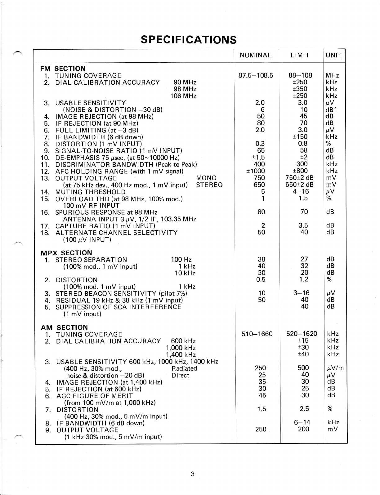
Realistic STA-85 User manual

ruLrstC.
Seruice
STA.85
AM /FM STEREO RECEIVER
Catalog Number:31 -2061
" cusloM MANUFACIURED FoB RADIo sHACK[|R orvrstoN 0F rANDy conponAloN

CONTENTS
SPECIFICATIONS 3 & 4
BLOCK D|AGRAM.......... ......................... 5
D|SASSEMBLY TNSTRUCTTONS ......... ................... 6
DIAL STRINGING DIAGRAM .............. 6
ALIGNMENTPROCEDURE 7_9
LEVEL DTAGRAM .......... ...................... 10
ALIGNMENT & CHECK POINTS .......... 11
TROUBLESHOOTTNG ............. .... 12 _ 16
0055 TUNER 8OARD................ . 17 & 18
6053 AUDTO AMp BOARD ........ 19 & 20
SEMICONDUCTOR LEAD IDENTIFICATIONS................. 21
ELECTRICAL PARTS LIST
MISCELLANEOUS PARTS LIST
SCHEMATIC DIAGRAM SEPARATE SHEET
EXPLODED VIEW SEPARATE SHEET
1.
2.
3.
4.
5.
6.
7.
8.
9.
10.
11.
12.
13.
14.
15.
22-29
30
,l

SPECIFICATIONS
NOMINAL LIMIT UNIT
FM SECTION
1. TUNING COVERAGE
2. DIAL CALIBRATION ACCURACY 90 MHz
98 MHz
3. usABLE sENsrrvrrY 106 MHz
(NOTSE & DTSTORTTON -30 dB)
4. IMAGE REJECTION (at 98 MHz)
5. lF REJECTION (at g0 MHz)
6. FULL LIMITING (at -3 dB)
7. lF BANDWIDTH (6 dB down)
8. DISTORTION (1 mV INPUT)
9. SIGNAL-TO-NOISE RATIO (1 mV INPUT)
10. DE-EMPHASIS 75 trrsec. (at 50-10000 Hz)
11. DISCRIMINATOR BANDWIDTH (Peak-to-Peak)
12. AFC HOLDING RANGE (with 1 mV signal)
13. OUTPUT VOLTAGE MONO
(at 75 kHz dev.,400 Hz mod., 1 mV input) STEREO
14, MUTING THRESHOLD
15. OVERLOAD THD (at 98 MHz, 100% mod.)
100 mV RF INPUT
16. SPURIOUS RESPONSE at 98 MHz
ANTENNA INPUT 3pV,1l2 1F,103.35 MHz
17. CAPTURE RATIO (1 mV INPUT)
18. ALTERNATE CHANNEL SELECTIVITY
(100 pV INPUT)
M PX SECTION
1. STEREO SEPARATION 100 Hz
(100% mod., 1 mV input) 1 kHz
10 kHz
2, DISTORTION
(100% mod. 1 mV input) 1 kl.{z
3. STEREO BEACON SENSITIVITY (pilot 7%)
4. RESIDUAL 19 kHz & 38 kHz (1 mV input)
5. SUPPRESSION OF SCA INTERFERENCE
(1 mV input)
AM SECTION
1. TUNING COVERAGE
2, DIAL CALIBRATION ACCURACY 600 KHZ
1,000 kHz
1,400 kHz
3. USABLE SENSITIVITY 600 kH2,1000 kHz, 1400 kHz
(400 H2,30% mod., Radiated
noise & distortion -20 dB) Direct
4. IMAGE REJECTION (at 1,400 kHz)
5. lF REJECTION (at 600 kHz)
6. AGC FIGURE OF MERIT
(from 100 mV/m at 1,000 kHz)
7, DISTORTION
(400 Hz, 30% mod., 5 mV/m input)
L IF BANDWIDTH (6 dB down)
9. OUTPUT VOLTAGE
(1 kHz 30% mod., 5 mV/m input)
87.5-108.5
0.3
65
r1.5
400
r1000
750
650
5
1
80
2.0
6
50
80
2.O
2
50
38
40
30
0.5
10
50
250
25
35
30
45
1.5
510-1660
250
88-108
t250
1350
r250
3.0
10
45
70
3.0
t1 50
0.8
58
!2
300
1800
75012 dB
650t2 dB
4-16
1.5
70
3.5
40
27
32
20
1.2
3-16
40
40
520-1620
r15
t30
t40
2.5
6-14
200
500
40
30
25
30
MHz
kHz
kHz
kHz
prV
dBf
dB
dB
pV
kHz
o/
/o
dB
dB
kHz
kHz
mV
mV
pV
o/
/o
dB
dB
dB
dB
o/
/o
dB
dB
kHz
kHz
kHz
kHz
pV lm
pV
dB
dB
dB
o/
/o
kHz
mV
pV
dB
dB

NOMINAL LIMIT UNIT
11.
12.
10. AUDIO RESPONSE
(5 mV/m input from 400 Hz to 3 kHz, 0 dB @1,000 kHz)
SELECTIVITY 200 pYlm
SIGNAL.TO-NOISE RATIO
(1000 kHz, with antenna input 5 mV/m)
AM BEAT (input 5 mV/m)
AUDIO SECTION
1. RMS OUTPUT POWER
(distortion (:0.3o/o,20 Hz - 20 kHz)
PER CHANNEL DRIVEN 8 O
BOTH CHANNELS DRIVEN 3 3
(lHF power @ 1 kHz,8 Sl, t1 dB)4 O
2. IM DISTORTION
(at 25 W output TO|T,OOAHz 411l
3. HARMONIC DISTORTION lat 25 W output)
100 Hz
1,000 Hz
10,000 Hz
4. FREOUENCY RESPONSE
(AUX, 8 Sl load, 1 W output, 30 Hz - 20 kHz)
5. INPUT SENSITIVITY (for 35 W output) PHONO
AUX
TAPE MON
PHONO
AUX
TAPE MON
BASS 100 Hz
TREBLE 10 kHz
8. EOUALIZATION RIAA: 30- 15,000 Hz
9. PHONO AMP OVER LOAD CAPABILITY (at 1%)
10. HIGH FILTER
11. LOUDNESS COMPENSATION (volume -30 dB)
12. CHANNEL SEPARATION
(AUX input 100 - 10,000 Hz)
13. SIcNAL-TO-NOISE RATTO (input shorted)
PHONO
AUX
14. RESIDUAL NOISE
15. LOAD IMPEDANCE
16. POWER SOURCE
20 WATTS, No Signal
170 WATTS, Full Signal
120 Volts,60 Hz AC*
13.
6. INPUT IMPEDANCE
7. TONE CONTROL
10 kHz
10 kHz
100 Hz
-4
28
40
50
55
40
45
0.2
0.1
0.1
o.2
r1
2.8
180
180
50K
70K
70K
r10
tg
120
-64
10
40
60
70
1.5
-6
20
32
10
40
45
35
35
0.5
0.15
0.15
0.3
r1.5
2.810.5
1 80r40
1 80r40
!10!2
!8!2
RIAAt2
100
-6!2
4!2
10t2
35
55
60
3
4-16
dB
dB
dB
o/
/o
W
W
W
W
o/
/o
o/
lo
o/
lo
o/
/o
dB
mV
mV
mV
ohm
ohm
ohm
dB
dB
dB
mV
dB
dB
dB
dB
dB
dB
mV
ohm
* 2201240 VAC, 50 Hz for European and Australian Models.
NOTE: Nominal Specs represent the design specs; all units should be able to approximate these-some
will exceed and some may drop slightly below these specs. Limit Specs represent the absolute
worst condition which still might be considered acceptable; in no case should a unit perform
to less than within any Limit Spec.
4

BLOCK DIAGRAM ;
o\
= E PH
i E-.dr =
E9 t-Jt A
E E:; *'E E
ee
H:=
==3
_l
E
al--=*= =:
ll
5
I
;
I+t't
=
t.F t't
=
33; =
==
z
=
LA- E--, -: :--.,]
:
=
<=e ==I
=r t
Er
-3
t
=:
=F
-= E3-
t==
AF
=F tEl
==
Es
at =
t- _-
==
ts= o I =,s
9l
t6
^_]
,*l
l
l
_l
I<F
zq;
6
t-
o=3
3! ,9
=
=---r-
I
I
I
___l_ 1
i; =
.l
i
l-r
t
=
=q
o-
Eo
---r
II
E
E
II
r
=
t=l
!l___l
_J&*
I
=
l
=<=
==
9=
Z6 ==
=a
E
2
==l
:l
-l =
=
=
V-)
E=
!==
=
E=E
7
l.
=9 )*l T
=
o
e
=
;=s =3
=9
=
cE
=-
E
E
=F
I
=
=oF
;> o
o
= : E= E:=:
g = E=E::=

DISASSEM BLY INSTRUCTIONS
1. Removing chassis from wooden cabinet. (Refer to Fig. A)
Remove the five screws (#58 & #66) from both sides of the wooden cabinet and back panel.
2. Removing the Front Panel. (Hefer to Fig. A)
a) Remove the knobs from SELECTOR, SPEAKERS, BASS, TREBLE, Tuning and VOLUME.
b) Remove six screws (#65) from both side of Front Panel and remove panel.
@
^(
rC
a, ^lA)
\D*
Fig. A@(B
DIAL STRINGING DIAGRAM
Note: Tuning capacitor should be in fully closed position.
{d
@-/:\
^_e
ar^
rurrnc srarr zf

ALIGNMENT PROCEDURES
Do not attempt alignment unless the following equipment is available.
Note: Remove line cord antenna from FM external antenna terminal
1. AM Signal Generator
2. Oscilloscope
3. AC Voltmeter
4. FM Signal Generator
5. Stereo Modulator
6. Audio Generator
7. Distortion meter
8. DC Voltmeter
9. Frequency Counter
when aligning.
AM IF & RF ALIGNMENT
RECEIVER
Loop Antenna
L451
Fis. 1 AM ALIGNMENT CONNECTION
TAPE OUT --l
Output of signal generator should be no higher than necessary to obtain an output reading.
Signal Generator Modulation: 30%
Set SELECTOR switch SWl to AM.
STEP SIGNAL
GENERATOR
COUPLING
SIGNAL
GENERATOR
FREOUENCY
R ECEIVER
DIAL
SETTING INDICATOR ADJUSTMENT
Refer Fig. 4. REMARKS
1Refer Fig. 1455 kHz
(400 Hz Mod.)
Point of non-
i nterference
(on/about
600 kHz)
AC Voltmeter
to TAPE OUT
jack T402 flFT) Adjust for maxi-
mum reading.
2Same as Step 1600 kHz
(400 Hz Mod.) 600 kHz Same as Step 1L402 (OSC Coil)
1451 (ANT Coil) Same as Step 1
3Same as Step 11400 kHz
(400 Hz Mod.) 1400 kHz Same as Step 1
TC1 05
(OSC Trimmer)
TC1 04
(ANT Trimmer)
Same as Step 1
4Same as Step 11000 kHz
(400 Hz Mod.) 1 000 kHz Same as Step 1vR402 Adjust for 160
mV Audio
output.
5Same as Step 11000 kHz
(400 Hz Mod.) 1000 kHz Receiver's
SIGNAL
Meter VR4O1 Adjust lor 70o/o
reading of full
scale with input
of 5 mV/m.
Note: Remove line cord antenna from FM external antenna terminal when aligning.
'7

FM RF AND IF ALIGNMENT
Zin = 50 o (75 o)
FM Dummy Antenna to 300 S) antenna terminal of Receiver
Zout = 3OO Sl (balanced)
8
Signal generator output should be no higher than necessary to obtain an output reading.
set selector switch to FM.
Signal Generator deviation: 75k{z NOTE: Be sure to disconnect FM line cord antenna during alignment.
STEP SIGNAL
GENERATOR
COUPLING
SIGNAL
GENERATOR
FREOUENCY
RECEIVER
DIAL
SETTING INDICATOR ADJUSTMENT
Refer Fig. 4. REMARKS
1
Connect to FM
Antenna Termi-
nal through
FM Dummy
Antenna
(300 O) Fig. 2
90 MHz
(400 Hz Mod.) 90 MHz
AC Voltmeter
connected to
TAPE OUT
jack
L101
(ANT. COIL)
L102
(RF COIL)
L 103
(OSC. COIL)
Adjust for maxi-
mum reading on
AC Voltmeter.
2Same as Step 1106 MHz
(400 Hz Mod.) 106 MHz Same as Step 1
TC1 O1
(ANT. Trimmer)
TC1O2 ,
(RF Trimmer)
TC1 03
(OSC. Trimmer)
Same as Step 1
Repeat steps 1 & 2 until no further improvement is possible.
3Same as Step 190 MHz
(400 Hz Mod.) 90 MHz Same as Step 1T101 flFT) Same as Step 1
4Same as Step 198 MHz
(400 Hz Mod.) 98 MHz DC Voltmeter
connect
across R21 1
(s.9 Ks,)
T201
(Bottom Core)
Adjust for zero
reading on DC
Voltmeter.
5Same as Step 198 MHz
(400 Hz Mod.) 98 MHz
Distortion
Meter con-
nected to
TAPE OUT
jack
T201
(Top Core) Adjust for mini-
mum distortion.
6Same as Step 198 MHz
(400 Hz Mod.) 98 MHz Receiver's
SIGNAL
Meter VR2O3 Adjust for 70o/o
reading of full
scale with input
of 1 mV.
7Same as Step 198 MHz
(400 Hz Mod.) 98 MHz
Oscilloscope
connect to
TAPE OUT
jack VR2O4
Adjust so output
just appears with
an input signal
level of 5 pV.
For European model, the lowest frequency of FM tuning range should not be below 87.5 MHz.
125 sl (112.5 s))
50 a (75 a)
150 r, Fis.2 FM DUMMY ANTENNA

MPX ALIGNMENT
TAPE OUT
FM ANTENNA
TE RM I NAL RECEIVER
(300 s,) tr-
Fig.3 MPX ALIGNMENT CONNECTION
MAIN AMPLIFIER ALIGNMENT
FRONT END
L103, L101
L102, TC101
TCl02, TC103
FM SIGNAL
GENERATOR FM DUMMY
ANTENNA
300 f2
FM IF
T201
VR2O3
vR2o,4
STEREO
MODULATOR
Set SELECTOR Switch to FM.
Tune for 98 MHz on band.
Signal Generator output level: 1000pV. Deviation: 75kHz, at 100% modulation of composite signal.
Connect Signal Generator to FM Antenna Terminal through FM Dummy Antenna (300 S.)).
ST EP
19 kHz
(PILOT SIGNAL)
MODULATION
Level
SIGNAL
GENERATOR
Freq. Set to
OUTPUT
INDICATOR
Connected to ADJUST
Refer Fig. 4ADJUST
FOR NOTE
18To Composite 1 kHz
R channel
AC Voltmeter to
TAPE OUT jack
of R channel
Adjust input for
audio output of
about 0.65 V
28% Composite
1 kHz L channel
AC Voltmeter to
TAPE OUT jack
of R channel VR301 Minimum
AC Voltmeter
reading shou ld
be at least 30
dB below reading
in step 1.
38Yo Composite
1 kHz R channel
AC Voltmeter to
TAPE OUT jack
of L channel VR301 Minimum Same as Step 2.
4PILOT OFF Carrier only
Frequency
Counter Connect
to TP (#10 pin)
of PCB 0055 and
ground
VR3O2 19 kHz
lf you did not obtain -30 dB readings in steps 2 and 3 (compared with step 1), readjust VR301 until you obtain -30 dB
reading for both steps 2 and 3.
INDICATOR ADJUSTMENT REMAR KS
DC Voltmeter VR601 a. bAdjust for 0.005 V - 0.015 V across
R623 a, b with no signal

LEVEL DIAGRAM
AUX : FM: AM SELECTOR
ctr
=,
=50
=
C9
UJ
(9 40
O
30
FRE0UENCY AT. 1 kHz
16.7V
35W/8s,
o
E'
cl
I
V
o
E
6l
(o
co
PH(]NO INPUT
10

ALIGNMENT & CHECK POINTS
L402
VR4O1
TC105
TC 104
TC101
TC102
TCl 03
T10l
VR2O3
VR2O4
TP
(N0.10 Pin)
V R302
FIGURE 4
NOTE: This Receiver has built-in over load thermal protection for abnormal operation.
When the temperature of the thermal protector (installed with heat sink) does rise abnormally
(9015'C), the thermal protector will automatically cut out, and as soon as the temperature goes
down suff iciently (35115'C), the thermal protector turns back on automatically.
lf the Receiver doesturn itself off, check ventilation and speaker connections.
L'101
L1 02
L1 03
Heat Sink of Power
Transistors POWE R
TRANSFORI\4ER
11
V8601 a
[-t-tl]r:tvl:
i& diPR0TEcr0R
AC OUTLET

TROUBLESHOOTING
SYMPTOM CAUSE AND REMEDY
1) Receiver not operative; pilot lamp
does not light. A) Faulty AC power cord
Replace the cord.
B) Defect in the power switch
Replace the switch.
C) Broken wire in the power transformer.
Replace the transformer.
D) Broken power fuse
Replace the fuse.
2l Fuse blows when power is turned on. A) Power Transformer T851 defective
Replace the transformer.
B) Short in the primary or secondary of the transformer
circuitry
Repair the short.
C) Damaged rectifier D801
Replace the rectifier.
D) Short-circuit in the rectifier circuit
Repair the short.
E) Short circuit in power transistor TR609a, b or
TR610a, b
Replace the defective transistor and check circuit.
3) Pilot lamp does not light. A) Defective lamp(s)
Replace lamp(s).
B) Open in the transformer T851 tertiary
winding
Replace the transformer.
4) Pilot lamp lights but no sound from
either channel. A) Resistor R801, R807, R508, R509, R904 0r R915
open
Replace.
B) Capacitor C507, C508, C801, C802, C807 or C808
defective
Rep lace the defective capacitor(s).
C) Diode D801 damaged
Replace the diode.
D) Open in secondary winding of the power trans-
former T851
Rep lace the transformer.
5) "A" Speakers do not work. A) Speaker switch SW8 defective
Replace the switch.
6) "B" Speakers do not work. A) Speaker switch SW8 defective
Replace the switch.
12

SYMPTOM CAUSE AND REMEDY
7l One channel does not work with
VOLUME at maximum, with a test
signal applied to the center terminal
of VOLUME control (VR551 or
VR552) of the dead channel.
A) Defect in transistor TR901, TR902 or TR903 of
Audio Amp Board 6053
Locate and correct the defect.
B) Defect in transistor TR601-TR610 of Audio Amp
Board 6053
Locate and correct the defect.
C) Break in copper foil of printed circuit board 6053
Repair or replace circuit board.
D) Short in speaker output terminal
Repair the short.
E) Defective resistor R903, R904, R906, R907, R914,
R915, R603-R606, R609, R610, R615, R620-R627
Replace the defective resistor(s).
8) Same as 7 above but channel
operates when test signal is applied
as 7.
A) Defective lC 1C501
Replace the lC.
B) Faulty resistor R503, R504, R508 or R509
Replace the faulty resistor(s).
C) Faulty capacitor C501 or C506
Replace the faulty capacitor(s).
D) Defective selector switch SW1
Repair or replace the switch.
9) Speaker works normally but head-
phones do not work. A) Headphone plug does not mate with jack
Replace the plug.
B) Defective resistor R629a, b
Replace the resistor.
10) All inputs work normally except
AUX input. A) Poor contact in AUX input jack
Repair or replace the jack.
B) Poor contact in selector switch SW1
Repair or replace the switch.
1 1) PHONO input not operative. A) Poor contact in PHONO input jack
Repair or replace the jack.
B) Faulty selector switch SW1
Repair or replace the switch.
C) Defective lC 1C501
Replace the lC.
12l, TAPE OUT not operative. A) Defective contact in TAPE OUT jack
Repair or replace the jack.
13

SYMPTOM CAUSE AND REMEDY
13) FM does not operate. A) Defective resistor R 107, R114, R207, R316, R317
or R235.
Replace the defective resistor(s).
Short circuit in Tuner B+ circuit
Repair the short.
Poor contact in selector switch SW1
Repair or replace the switch.
Defective diode D201
Replace the diode.
Capacitor C301 defective
Replace the capacitor.
Defective transistor TR201 or lC 1C201
Replace the defective component.
Defective IFT T201
Replace the lFT.
Defective capacitor C2 1 1
Replace the capacitor.
Defective transistor TR 101, TR 102, TR 103 or Coil
L101, L1O2, Ll03 of Tuner Board 0055
Replace the defective component(s).
Faulty lead-in
Repair or replace the lead-in.
B}
c)
D)
E)
F)
G)
H)
t)
J)
14l Poor multiplex separation A) lmproper adjustment
Readjust T2O1, VR301 and VR302.
(Refer to MPX ALIGNMENT on page 9)
B) Defective lC 1C301
Replace the lC.
C) Variable resistor VR301 or VR302 defective.
Replace the variable resistor(s).
15) Stereo indicator does not light. A) Defective LED D303
Replace the LED.
B) Defective lC 1C301 or resistor R322 of Tuner board
0055
Replace the defective component(s) .
C) Defective diode D301
Replace the diode.
16) FM volume not sufficient. A) lf volume of both L and R channels not enough
Front End defective, or faulty transistor TR201
lC 1C201, IFT T201 or diode D2O3, capacitor
C211 or faulty TR301, TR302, tC301 or C301
of Tuner Board 0055
Replace the defective component(s).
B) lf sound of one channel not enough: Defective
L301 in case of L channel, or defective L302 in
case of R channel
Replace the defective coil.
14

SYMPTOM CAUSE AND REMEDY
17l AM does not operate. Damaged 1C401 of Tuner Board 0055
Replace 1C401.
Defective L4O1, L404, T401 or T4O2 of Tuner
Board 0055
Replace the defective component(s).
Defective diode D401 or D4O2 of Tuner Board 0055
Replace the defective diode(s).
One of resistors of Tuner Board 0055
Replace the defective part.
One of capacitors of Tuner Board 0055
Replace the defective part.
Selector switch SW1 defective
Repair or replace the switch.
Defective Tuning Gang
Replace Tuning Gang.
Damaged AM bar antenna
Repair or replace the bar antenna.
A)
B)
c)
D)
E)
F)
G)
H)
18) LOUDNESS has no effect. A) Defective LOUDNESS Switch SWs
Replace the switch.
B) Defective C701 or R703
Replace defective component(s).
C) Defective VOLUME control VR551 or VR552
Replace.
19) STEREO-MONO not effective A) Defective MONO switch SW4
Replace the switch.
2Ol TAPE MONITOR noteffective A) Defective TAPE MON switch SW3
Replace the switch.
B) Poor contact in TAPE lN input jacks
Repair or replace jack.
C) Resistor R702 defective
Replace the resistor.
21!. BASS control has no effect. A) VR902 defective
Replace.
B) Defective C908, C909 or R908, R910, R912 of
Audio Amp Board 6053.
Replace the defective component(s).
221 TREBLE control has no effect. A) VR901 defective
Replace.
B) Defective C906, C907, R909, R91 1, R913 of
Audio Amp Board 6053
Replace the defective component(s).
23t. Excessive noise with PHONO input A)
B)
Faulty lC 1C501
Replace the lC.
Faulty R501, R503, R504 or C501, C506
Replace the faulty component(s).
15

SYMPTOM CAUSE AND REMEDY
24l, Noisy VOLUME control A) Defective VR551 or VR552
Replace the variable resistor.
B) Defective capacitor C506, C901, C905 or C912
Replace the defective capacitor(s).
25l. SIGNAL meter not functioning. A) Defective meter
Replace the meter.
B) ln case of FM reception, lC2O1, D2O4 or TH201
defective
Replace the defective component(s).
C) ln case of AM reception, 1C401 or VR401 defective
Replace the defective component(s).
26l, AUTO-MAGIC AFC has no effect
when AUTO-M switch is ON.
(White light behind the tuning meter
does not change to red when the
tuning control is touched.)
A) Transistor TR701 ,TR7O2 or lC 1C701 defective
Replace the defective component(s).
B) Resistor R706, R715, R716 or R718 defective
Replace the defective resistor(s).
C) Diode D7O1, D7O2 or D852 defective
Replace the defective diode(s).
D) Capacitor C7O4 or C705 defective
Replace the defective capacitor(s).
E) Defective switch SW2.
Replace the switch.
271 Red light does not light when the
tuning control is released. A) Defective transistor TR701 (open) or TR702 (short)
Replace the defective transistor(s).
281 Hl-FlL has no effect. A) Defective switch SW6
Replace the switch.
B) Defective capacitor C702
Replace the capacitor.
NOTE:
Transistors TR605 and TR606 protect the audio output stage when abnormally high current flows through
TR609 and TR610, caused by excessive drive at input, or too low impedance load is connected at output.
lf increase of the current is excessive, the voltage across R623 and R626 will turn on TR605 and TR606
which are normally not biased "on".
The collector potential of these transistors (through D601 and D602 diodes) reduce bias on TR607 and
TR608, which causes output transistor current (TR609 and TR610) to reduce.
This performs two safety functions.
1. Protects the output circuit devices.
2. Protects the speakers from loud clicks, pops and
excessive levels.
TO OBIVT
CIBCUIT
TO OBIVT
CIRCUIT
16

OO55 TUNER BOAI
/::l 1\
(v f.)e"
\:t/. :r. ,i
]6=
\7
@. .-.c
E m irsl
':::lj:j
I :, ll,,
{:'L
)= )z
-i) 'rx
C.Ol.
,"', ,' .,.,(jJ,*, 'ffi
{@
.'.'..,,...'..r.)-
6)* i
- (rr
O*^
- f.rH
\J
,'.111
,**Lis
Fi+.,,+,i5'a',,,
€rn1
,r-
,
No )= \
v
u I- ) n
tHA^ll I
|(
+l{
xJUV A=I=
EX/
VE f;.
; \t
l; E'
t^
\_,9
)a=-+
E -isr
- t3./ ,
- jo) a\
'{,'
fs ri?!4 x())
@"ffi : *,; 'iiri '., '
;3 . rmr )-,-
"{oP#r
-E- EIJA
iz C322 \^UA
f.iY'? = \ '
). \*EE/ 6
ptft:
E) ="(, G
./ 71
fr304 5 6K \ ,mrrc li
hr,, \nizd,
I rnnv+I2q(1i
\4v?
= l;-
3 l5q
= l---i
=i ffi
E A l- lbrr5o '-'
=d/ :>..:r/ap ,
E-)*:t \7X**3-F=c'
]
(q;sl.
\+,+
at' i
4a.\ ;= .;>
rrffii
n:zr sl -') t
e
+aB
::- ::-
!t \:,",11.,'i) %n*lffT )
3
e
tqP
P:\
R219.220( *:
lE.E)
lqi
I l,
-?B ,LI /:T_
i:\ H i /
Es Xl--.-*
- { B2os r5oK ) i
ni* D
--l-E :'
'*!q rd
I E - L-..0.1
ffi
8?t 1...,5. )1
ffi >'J BZoB ..,i50
?07
.B
ltt_t
ll l;!l
L] [*=l
r'icirir.:.. ..::' - o
LAll3ol',,.i..;r' ",:r:
ll x!!li,.}
ll (oI<..g*,,2-
H2l8 l80K b< 0 u /
Elln"I '
l:Hl^
t" l/es
t8s
.*: \,,
/'\ .-
1-t\ 1 nz:r 'o
v-- ,o'rt4
' lt d o
---at ::
17

UNER BOARD (TOP VIEW)
:@
@i'

OO55 TUNER BOARD (BOTI
I, ,ll].,,,.,
lrr,,,,o*, -1- e71t ?7k -L ^- =ls .02&>lKB"62 'fH G
L*lqL ,s+* O*O' ..',,,....'..,l:tt:,.,.',1' ;; 'i{!,',. .'3+f !l#1'!,,;,,:,-?,,-, ,.;;:
---:J5-9----.-.---"-..\-.--__-..fc?,iEflji'Et*ffic
Pig---i1 C= --- t= i ._. : I I* , _r..iif1ti, * ;iij_-= is - =
H*llue €. f i.=.:ifil Hl;.i-j{-ri"};=rijs 1,,_ =l
* lJ l= k I= (D- *;**ri, t . c21s _'#f*g' :i,g J= 1I' \'
llY-*--'-"f' x t- is ,^ ^ fl=^,-\ ,^c?12 004 ,." i
L_'__t__'__l ,^ L--r- @.ol.aaaa- I 'ciT
.-rzt*lo. ' . c21s_ _'i"d+i"iT#' jilT J= 1I' \'
*4+sr{ 1222 - **ffii:W$pffi4.f- ;-rr,r
. r!9sl?!!. .{tr{^,mi. T J. ""',i:r ' pzos v<ox'ia i =:r
^ l.-IE c21so16ov rf- -? I --
W^^?.^ !l! .+:j' -o,, :. ;fi!G-----t I .lq.
t ,a* _. I r -:B c21s o16ov i r t -? L;";
,,,,,,,,,,,,,,',,.1.,:,,.',,,., . :ffi""luH**l- I=a . =+EF$1:;&*'o.}',fn" 3',,,,.'1,.,'1,#
i+ii*- ?-1=.:r:u l- ',;--. E*l .nzrr*s'x:*-: ili =
3; ;.t =-l,F;f-=l= i= Etu riat l --=1* i--,ru-' | .i-'-,
?E 1 "ai#!E i't L;;-., \---,'q+:i- ll*yt/^ l- -_*
a a=
\ aa
a_1e
I uri,?ifii
,i,'i:{..-a' {qr3
iih vit:O=
=s:ffi=1n6.
,_-z *1 .-t+- V Rip.uli*!
3!E oo'(oi.!?l!*91- r.l-'ioo cr2r 0'r'50!
*tii I,LHgt*: **ffi.
1." le ,----il l';
fl-t ''ffi.ry$
fxp '*Gr!: '.!ffi=tti.1 1\,*:Hq# "ffi
-l '; T--'-;*;1e+F.l*- l-.* .f '-rYl-? : 4:V = I*l*
,Liffg._ffb- ,io-, , l*' .. i l=tit= 41+=*=
l; Iiit'I mJil:t ,,:'',,'"* ,, ..,'':' .:",-- ';J$*.'i i="= H; .r
f= t-r,,..-,.rr^ 'j'#' \]/- . r '', ,' , - . ! ,' '-,'=
c1$ ee
L-
at
)
l
t-
t:
I

ID (BOTTOM VIEW)
ts
,[,,i*-J
,lr,e,it
,l;Jl
,1i,'l''ll
,,ii l.rr
.l:+,Jl],'
| --1
l.-'l
,lt?r,il:
l:,?,r.11
rli-ll
l--J
,.f*t,.
,1,;.,.;
,i,;-],.,1
l*--/
t-J
1B
This manual suits for next models
1
Table of contents
Other Realistic Stereo Receiver manuals

Realistic
Realistic STA-95 User manual

Realistic
Realistic STA-95 User manual

Realistic
Realistic STA-2100D User manual

Realistic
Realistic STA-21 User manual

Realistic
Realistic STA-720 User manual

Realistic
Realistic STA-78 User manual

Realistic
Realistic STA-235 User manual

Realistic
Realistic STA-7 User manual

Realistic
Realistic STA-115 User manual

Realistic
Realistic 31-2080 User manual