R16UZ0031EU0100 Rev.1.00 Page 4
Apr 1, 2022
ISL9123IIx-EVZ, ISL9123IRx-EVZ Evaluation Board Manual
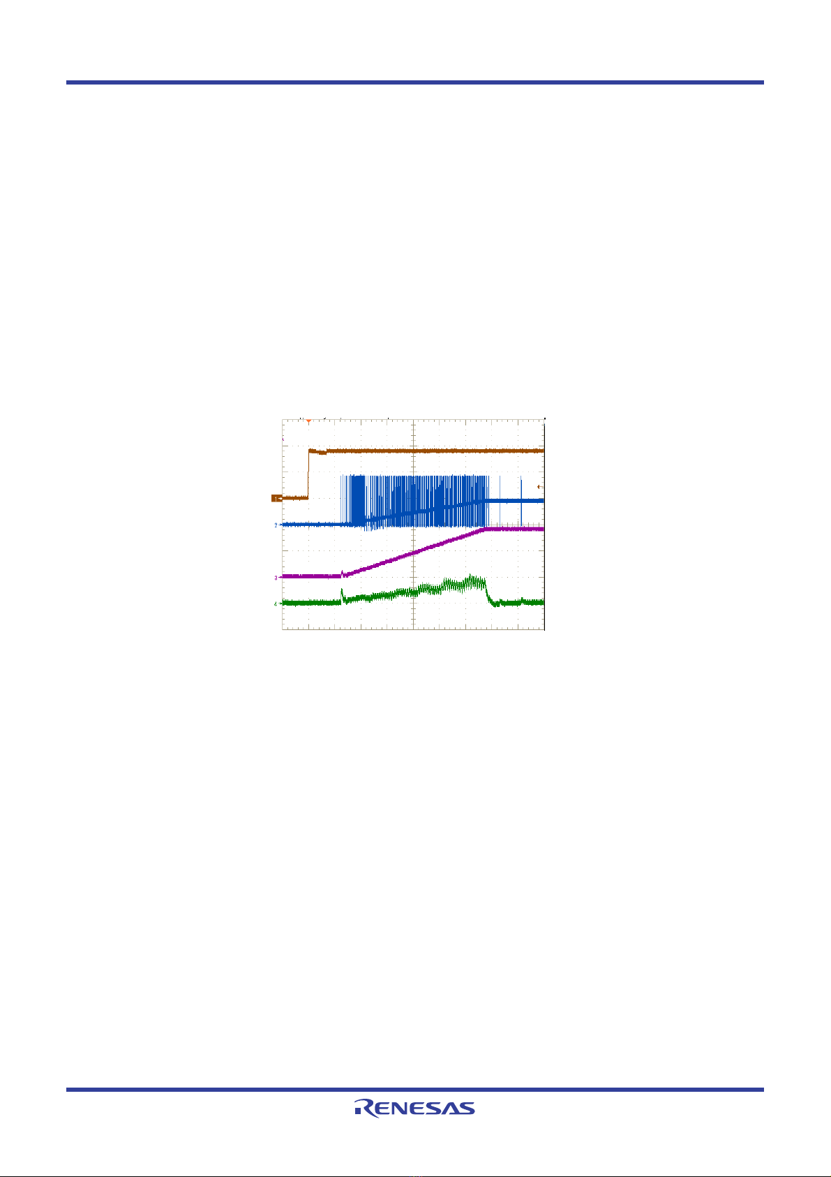
5. Turn on the power supply. At the end of the soft-start sequence, the ISL9123 is operating in Regulation mode
at default output voltage setting. Note: A minimum effective output capacitance of 6µF is required. Therefore,
depending on the performance specifications of the capacitor, an additional output capacitor might be required
for higher output voltage settings.
6. Monitor the output voltage start-up sequence on the scope. The waveforms should look similar to those shown
in Figure 2.
7. Turn on the electronic load.
8. Measure the output voltage with the voltmeter. The voltage should regulate within the datasheet specification
limits.
9. To determine efficiency, measure input and output voltages at the Kelvin sense test points (S+ and S-), which
are part of J1 and J2 headers. The bench power supply can be connected to the VIN and GND headers on J1.
The electronic load can be connected to the VOUT and GND headers on J2. Measure the input and output
currents. Calculate the efficiency based on these measurements.
10. VSW (auxiliary output) should be left floating if not connected to a load. Refer the part datasheet for additional
information on VSW pin.
1.3 Evaluation Software Installation and Use
The ISL9123 evaluation software and evaluation software guide are available for download from the Renesas
website.
1. Save the evaluation software executable file and install the evaluation software (see the evaluation software
manual). When the evaluation software launches, (see the Setup and Configuration and) connect the power
supply, DC load, and other test equipment to the evaluation board; next, apply power.
2. The ISL9123 has five control registers. See the ISL9123 datasheet for detailed register descriptions.
3. Register RO_REG1 (Address: 0x02) provides chip identification information. The Get IC INFO_RO_REG1
button reads from this read-only register.
4. To change the output voltage, you can use the VSET Control slider in the VSET register (Address: 0x11) panel
and perform a Write REG operation. The output voltage ramps up at the slew rate specified in the DVSRATE
setting of CONV_CFG register. If the modified output voltage is lower than the initial value, its ramp down rate
depends on the applied load and output capacitance. The Read REG button provides the contents of the
register, so adjust the slider accordingly.
5. Register INTFLG_REG (Address: 0x03) contains the fault flags. The background color changes from green to
red: when (1) a fault occurs, and (2) this register is read using either the Check Fault button or the READ ALL
button. Each bit is set by a fault event and cleared when read. When the bit is cleared after reading, the
background color changes from red back to green.
Figure 2. ISL9123 Start-Up with VIN = 3.6V and VOUT = 1.8V
OUT
IIN