manuals.online logo
Brands
  1. Home
  2. •
  3. Brands
  4. •
  5. Rohm
  6. •
  7. Microcontroller
  8. •
  9. Rohm LAPIS ML610Q305 User manual

Rohm LAPIS ML610Q305 User manual

FEDL610Q306-03
Issue Date: Aug. 7, 2023
ML610Q305/306
8-bit Microcontroller with Voice Output Function
1/36
GENERAL DESCRIPTION
ŸPlease see the “Notes” and the “Notes for product usage” in this document.
Equipped with a 8-bit CPU nX-U8/100, the ML610Q305/306 is a high-performance 8-bit CMOS microcontroller that integrates
a wide variety of peripherals such as timer, synchronous serial port, successive approximation type 10-bit A/D converter and
voice output function. The nX-U8/100 CPU is capable of executing instructions efficiently on a
one-instruction-per-clock-pulse basis through parallel processing by the 3-stage pipelined architecture. The ML610Q305/306
is also equipped with a flash memory* that has achieved low voltage and low power consumption (at read) equivalent to mask
ROM, so it is best suited to battery-driven applications such as alarm and portable devices. In addition, it has an on-chip
debugging function, which allows software debugging/rewriting with the LSI mounted on the board.
FEATURES
•CPU
−8-bit RISC CPU (CPU name: nX-U8/100)
−Instruction system: 16-bit instructions
−Instruction set: Transfer, arithmetic operations, comparison, logic operations, multiplication/division, bit
manipulations, bit logic operations, jump, conditional jump, call return stack manipulations, arithmetic shift, and so on
−On-Chip debug function
−Minimum instruction execution time
Approx 30.5 µs (@32.768kHz system clock)
Approx 0.244 µs (@4.096 MHz system clock)@VDD=2.0 to 5.5V
Approx 0.122 µs (@8.192 MHz system clock)@VDD=2.2 to 5.5V
•Internal memory
−Has 96-Kbyte flash ROM(48K ×16-bits) built in. (1 K byte of test domain that it cannot be used is included)
−Has 2-Kbyte flash ROM built in. (area in which self rewriting is possible (512byte ×4))
−Internal 1Kbyte RAM (1K ×8 bits)
•Interrupt controller
−2 non-maskable interrupt sources
Internal source: 1(Watchdog timer)
External source: 1(NMI)
−24 maskable interrupt sources
Internal source: 16(SSIO0, SSIO1, UART, I2C bus master/slave interface, Timer 0, Timer 1, Timer 2, Timer 3,
A/D converter, Voice sound reproduction, Speaker pin short detection, TBC128Hz, TBC32Hz,
TBC16Hz, TBC2Hz)
External source: 8(P80, P81, P82, P83, P84, P85, P86, P87)
•Time base counter
−Low-speed time base counter ×1 channel
−High-speed time base counter ×1 channel
•Watchdog timer
−Generates a non-maskable interrupt upon the first overflow and a system reset occurs upon the second
−Free running
−Overflow period: 4 types selectable (125ms, 500ms, 2s, and 8s at 32.768kHz)
*: This product uses SuperFlash® technology licensed from Silicon Storage Technology, Inc. SuperFlash®
is a registered trademark of Silicon Storage Technology, Inc.
FEDL610Q306-03
ML610Q305/306
2/36
•Timers
−8 bits ×4ch (16-bit configuration available)
•Voice output function
−Voice synthesis method: 4-bit ADPCM2 / non-linear 8-bit PCM / straight 8-bit PCM /
straight 16-bit PCM / HQ-ADPCM
−Sampling frequency: 8kHz, 16kHz, 32 kHz, 10.7kHz, 21.3 kHz, 6.4kHz, 12.8kHz, 25.6 kHz
•Successive approximation type A/D converter
−10-bit A/D converter
−Input: 3ch (ch0-2:External input) (for ML610Q305) /
4ch (ch0-3:External input) (for ML610Q306)
−Conversion time: 24.4 μs per channel at 4.096MHz VDD≥2.2V
−Conversion time: 12.2 μs per channel at 8.192MHz VDD≥2.5V
−Continuous conversion / Single conversion selectable
•Synchronous serial port
−2ch
−Master/slave selectable
−LSB first/MSB first selectable
−8-bit length/16-bit length selectable
•UART
−Half-duplex × 1ch
−TXD/RXD
−Bit length, parity/no parity, odd parity/even parity, 1 stop bit/2 stop bits
−Positive logic/negative logic selectable
−Built-in baud rate generator
•I2C bus interface
−Master function: standard mode (100 kbps) and Fast mode (400 kbps)
−Slave function: standard mode (100 kbps) and Fast mode (400 kbps)
•General-purpose ports
−Input-only port ×1ch
−Output-only port ×3ch (including secondary functions)
−Input/output port ×12ch (including secondary functions)
(P40 to P42 uses also as an A/D converter input port.) (for ML610Q305)
×15ch (including secondary functions)
(P40 to P43 uses also as an A/D converter input port.) (for ML610Q306)
•Speaker amplifier(D-class) output power
−1.0W(at 5.0V)/0.45W(at 3.0V)
−Disconnection detection circuit
−Speaker pin short detection circuit
•Reset
−Reset through the RESET_N pin
−Power-on reset generation when powered on
−Reset by the watchdog timer (WDT) overflow
−PLL oscillation stop detection reset
−Low level detection (LLD) reset
•Clock
−Low-speed clock
Built-in RC oscillation (32.768 kHz)
−High-speed clock
Built-in PLL oscillation (Approx. 1.024MHz / 2.048MHz / 4.096MHz / 8.192MHz)
FEDL610Q306-03
ML610Q305/306
3/36
•Power management
−STOP mode: Stop of oscillation (Operations of CPU and peripheral circuits are stopped.)
−HALT mode: Instruction execution by CPU is suspended (peripheral circuits are in operating states).
−Clock gear: The frequency of high-speed system clock can be changed by software (1/2, 1/4, 1/8, or 1/16 of the
oscillation clock)
−Block control function: Operation of an intact functional block circuit is powerd down. (register reset and clock stop)
•Shipment
−32-pin WQFN(P-WQFN32-0505-0.50-A63)
ML610Q305-xxxGD (blank product: ML610Q305-NNNGD)
−32-pin TQFP(P-TQFP32-0707-0.80-ZK6 or P-TQFP32-0707-0.80-Z6K6)
ML610Q305-xxxTB (blank product: ML610Q305-NNNTB)
−36-pin WQFN(P-WQFN36-0606-0.50-A63)
ML610Q306-xxxGD (blank product: ML610Q306-NNNGD)
xxx: ROM code number
•Guaranteed operating range
−Operating temperature: −40°C to 85°C
−Operating voltage: VDD = 2.0V to 5.5V, SPVDD = 2.0V to 5.5V
FEDL610Q306-03
ML610Q305/306
4/36
BLOCK DIAGRAM
ML610Q305/306 Block Diagram
* : Secondary or tertiary function
*1:Select I/O port or A/D converter input terminal
Program Memory
(Flash)
96Kbyte
Data Flash
2Kbyte
RAM
1KByte
Interrupt
Controller
CPU (nX-U8/100)
Timing
Controller
EA
SP
Instruction
Decoder
BUS
Controller
Instruction
Register
TBC
INT
4
INT
4
8bit Timer
Data-bus
TEST0
RESET_N
OSC
POWER
VDDL
RESET &
TEST
ALU
EPSW1
~
3
PSW
ELR1
~
3
LR
ECSR1
~
3
DSR/CSR
PC
GREG
0~15
VDD
VSS
On-Chip
ICE
SSIO
SCK0*
SIN0*
SOUT0*
INT
2
WDT
INT
1
INT
2
10bit-ADC
VREF
1
INT
LSCLK*
OUTCLK*
VOICECNT
SCK1*
SIN1*
SOUT1*
SPP
SPM
TEST1_N
LLD
SPVSS
SPVDD
AIN0 to AIN2*1 (Q305)
or
AIN0 to AIN3
*1(Q306)
GPIO
INT
9
I2C
Master/Slave
INT
2
SDA*
SCL*
50 to P57
D-class
Speaker
Amplifier
UART
INT
1
RXD0*
TXD0*
P80 to P87
P40 to P42*1(Q305) or
P
40 to P431 (Q306)
P20 to P22
NMI
P90(Q305) or
P90 to P92(Q306
)
FEDL610Q306-03
ML610Q305/306
5/36
PIN CONFIGURATION
Pin Layout of ML610Q305 32pin WQFN Package(Top View)
P22/LED2 1
V
SS
3
P20/LED0 4
P80/EXI0/SDA/SIN0 5
P81/EXI1/SCL/SCK0 6
TEST1_N 7
9TEST0
10 P82/EXI2/SOUT0
15 SPM
14 SPP
12 RESET_N
11 P83/EXI3
16 SPM
NMI 32
P87/EXI7/TXD0 31
P41/AIN1/SCK1/SCK0 27
P40/AIN0/SIN1/SIN0 28
V
REF
29
P86/EXI6/RXD0/SOUT1 30
P42/AIN2/SOUT1/SOUT0 26
24 V
DDL
23 V
SS
22 P85/EXI5/SCK1
21 P84/EXI4/SIN1
19 SPV
DD
17 SPV
SS
P21/LED1 2
(TOP VIEW)
WQFN32
P90 8
13 SPP
V
DD
25
18 SPV
SS
20 SPV
DD
FEDL610Q306-03
ML610Q305/306
6/36
Pin Layout of ML610Q305 32pin TQFP Package(Top View)
P42/AIN2/SOUT1/SOUT0
(
TOP VIEW
)
TQFP32
25
26
27
28
29
30
31
32
1
2
3
4
5
6
7
8
16
15
14
13
12
11
10
9
SPM
SPM
SPP
SPP
RESET_N
P83/EXI3
P82/EXI2/SOUT0
TEST0
24
23
22
21
20
19
18
17
SPVDD
SPV
SS
SPV
SS
P22/LED2
P21/LED1
VSS
P20/LED
P80/EXI0/SDA/SIN0
P81/EXI1/SCL/SCK0
TEST1_N
P90
P40/AIN0/SIN1/SIN0
P41/AIN1/SCK1/SCK0
P85/EXI5/SCK1
P84/EXI4/SIN1
VDD
NMI
P87/EXI7/TXD0
P86/EXI6/RXD0/SOUT1
VREF
V
DDL
SPV
DD
V
SS
FEDL610Q306-03
ML610Q305/306
7/36
Pin Layout of ML610Q306 36pin WQFN Package(Top View)
(NC): No Connection
P20/LED0 5
11 TEST0
P86/EXI6/RXD0/SOUT1 34
25 P92
P91 1
P21/LED13
V
SS
4
P80/EXI0/SDA/SIN0 6
P81/EXI1/SCL/SCK0 7
NMI 36
P87/EXI7/TXD0 35
P41/AIN1/SCK1/SCK0 31
P40/AIN0/SIN1/SIN0 32
V
REF
33
P42/AIN2/SOUT1/SOUT0 30
P22/LED2 2
(TOP VIEW)
WQFN36
TEST1_N 8
P43/AIN3 29
P90 9
18 SPM
V
DD
28
10 (NC)
17 SPM
16 SPP
15 SPP
13 P83/EXI3
12 P82/EXI2/SOUT0
14 RESET_N
24 P85/EXI5/SCK1
23 P84/EXI4/SIN1
22 SPV
DD
21 SPV
DD
20 SPV
SS
19 SPV
SS
27 V
DDL
26 V
SS
FEDL610Q306-03
ML610Q305/306
8/36
LIST OF PIN
In the I/O column, “—” denotes a power pin, “I” an input pin, “O” an output pin, and “I/O” an input/output pin.
36pin
WQFN
32pin
WQFN
/TQFP
Primary function
Secondary/Tertiary function
Pin name I/O Description
Secondary/
Tertiary
Pin name I/O Description
15, 16 13, 14 SPP O
Positive output pin of the
built-in speaker amplifier


17, 18 15, 16 SPM O
Negative output pin of the
built-in speaker

19, 20 17, 18 SPVss 
Negative power supply pin for
built-in speaker amplifier

21, 22 19, 20 SPVDD 
Positive power supply pin for
built-in speaker amplifier

4, 26
3, 23
VSS

Negative power supply pin




27 24 VDDL 
Power supply for internal logic
(internally generated)

28
25
VDD

Positive power supply pin




33 29 VREF 
Reference power supply pin
for successive-approximation
type ADC
   
14
12
RESET_N
I
Reset input pin




11
9
TEST0
I/O
Input/output pin for testing




8
7
TEST1_N
I
Input pin for testing




36 32 NMI I
Input port,
non-maskable interrupt
   
5
4
P20/LED0
O
Output port / LED port
Secondary
LSCLK
O
Low-speed clock output
3
2
P21/LED1
O
Output port / LED port
Secondary
OUTCLK
O
high-speed clock output
2
1
P22/LED2
O
Output port / LED port




9
8
P90
I/O
Input port/Output port




1

P91
I/O
Input port/Output port




25

P92
I/O
Input port/Output port




32 28 P40/AIN0 I/O
Input port/Output port
/Successive-approximation
type ADC input0
Secondary SIN1 I SSIO1 data input
Tertiary SIN0 I SSIO0 data input
31 27 P41/AIN1 I/O
Input port/Output port
/Successive-approximation
type ADC input1
Secondary SCK1 I/O SSIO1 clock input/output
Tertiary SCK0 I/O SSIO0 clock input/output
30 26 P42/AIN2 I/O
Input port/Output port
/Successive-approximation
type ADC input2
Secondary SOUT1 O SSIO1 data output
Tertiary SOUT0 O SSIO0 data output
29 P43/AIN3 I/O
Input port/Output port
/Successive-approximation
type ADC input3

6 5 P80/EXI0 I/O
Input port/Output port /
External interrupt
Secondary
SDA
I/O
I2C data input/ output
Tertiary
SIN0
I
SSIO0 data input
7 6 P81/EXI1 I/O
Input port/Output port /
External interrupt
Secondary
SCL
I/O
I2C clock input/output
Tertiary
SCK0
I/O
SSIO0 clock input/output
12 10 P82/EXI2 I/O
Input port/Output port /
External interrupt
Tertiary SOUT0 O SSIO0 data output
13 11 P83/EXI3 I/O Input port/Output port /
External interrupt
  
23 21 P84/EXI4 I/O
Input port/Output port /
External interrupt
Tertiary SIN1 I SSIO1 data input
24 22 P85/EXI5 I/O
Input port/Output port /
External interrupt
Tertiary SCK1 I/O SSIO1 clock input/output
34 30 P86/EXI6 I/O
Input port/Output port /
External interrupt
Secondary
RXD0
I
UART0 data input
Tertiary
SOUT1
O
SSIO1 data output
35 31 P87/EXI7 I/O
Input port/Output port /
External interrupt
Secondary TXD0 O UART0 data output
Note:
The function which is not chosen is lost when either a secondary function or a tertiary function is chosen. However, when
using it as an input, read-out of an input data is possible at a port n data register (PnD).
FEDL610Q306-03
ML610Q305/306
9/36
PIN DESCRIPTION
In the I/O column, “—” denotes a power pin, “I” an input pin, “O” an output pin, and “I/O” an input/output pin.
Pin name I/O Description
Primary/
Secondary/
Tertiary
Logic
Power supply
V
SS
—
Negative power supply pin
—
—
V
DD
—
Positive power supply pin
—
—
V
DDL
—
Positive power supply pin for internal logic (internally generated)
Connect the capacitor CL(1uF)( Refer to Measuring circuit 1) to
VSS
—
—
SPV
SS
—
Negative power supply pin for built-in speaker amplifier
—
—
SPV
DD
—
Positive power supply pin for built-in speaker amplifier
—
—
V
REF
—
Reference power supply pin for successive-approximation type ADC
—
—
Test
TEST0
I/O
Input/output pin for testing. Has a pull-down resistor built in.
—
Positive
TEST1_N
I
Input pin for testing. Has a pull-up resistor built in.
—
Negative
System
RESET_N I
Reset input pin
. When this pin is set to a “L”level, the device is
placed in system reset mode and the internal circuit is initialized
.
If after that this pin is set to a “H”level, program execution starts
.
This pin has a pull-up resistor built in.
— Negative
LSCLK O
Low-speed clock output. This function is allocated to the secondary
function of the P20 pin.
Secondary —
OUTCLK O High-speed clock output. This function is allocated to the secondary
function of the P21 pin.
Secondary —
General-purpose Output port
P20 to P22 O
General-purpose output ports.
Provided with a secondary function. Cannot be used as ports if
their secondary function is used.
Primary Positive
General-purpose Input/output port
P40 to P42 I/O
General-purpose input/output ports.
Provided with a tertiary function. Cannot be
used as ports if their
tertiary function is used.
Primary Positive
P43
I/O
General-purpose input/output port. (built into ML610Q306)
Primary Positive
P80 to P87 I/O
General-purpose input/output ports.
Provided with a secondary function or a tertiary func
tion. Cannot
be used as ports if their secondary function or tertiary function is
used.
Primary Positive
P90
I/O
General-purpose input/output ports.
Primary Positive
P91 to P92
I/O
General-purpose input/output port. (built into ML610Q306)
Primary
Positive
FEDL610Q306-03
ML610Q305/306
10/36
Pin name I/O Description
Primary/
Secondary/
Tertiary
Logic
I
2
C bus interface
SDA I/O
I2C data input/output pin. This pin is used as the secondary
function of the P80 pin. This pin has an Nch open drain output.
When using this pin as a function of the I2C
, externally connect a
pull-up resistor.
Secondary Positive
SCL I/O
I2C clock output pin. This pin is used as the secondary function
of the P81 pin. This pin has an Nch open drain output. When
using this pin as a function of the I2C, externally connect a
pull-up resistor.
Secondary Positive
Synchronous serial (SSIO)
SIN0 I
Synchronous serial data input pin. Allocated to the tertiary
function of the P40 pin and P80 pin.
Tertiary Positive
SCK0 I/O
Synchronous serial clock input/output pin. Allocated to the
tertiary function of the P41 pin and P81 pin.
Tertiary —
SOUT0 O
Synchronous serial data output pin. Allocated to the tertiary
function of the P42 pin and P82 pin.
Tertiary Positive
SIN1 I
Synchronous serial data input pin. Allocated to the tertiary
function of the P84 pin and the secondary function of the P40
pin.
Secondary/
Tertiary Positive
SCK1 I/O
Synchronous serial clock input/output pin. Allocated to the
tertiary function of the P85 pin and the secondary func
tion of the
P41 pin.
Secondary/
Tertiary —
SOUT1 O
Synchronous serial data output pin. Allocated to the tertiary
function of the P86 pin and the secondary function of the P42
pin.
Secondary/
Tertiary Positive
UART
TXD0 O
UART data output pin. Allocated to the secondary function of the
P87 pin.
Secondary Positive
RXD0 I
UART data input pin. Allocated to the secondary function of the
P86 pin.
Secondary Positive
External interrupt
NMI I
External non-maskable interrupt input pin. The interrupt occurs
on both the rising and falling edges.
Primary Positive/
Negative
EXI0 to 7 I
External maskable interrupt input pins. It is possible, for each bit,
to specify whether the interrupt is enabled and select the
interrupt edge by software. Allocated to the primary function of
the P80 to P87 pins.
Primary Positive/
Negative
LED drive
LED0 to 2 O
Pins for LED driving. Allocated to the primary function of the P20
to P22 pins.
Primary Positive/
Negative
Voice output function
SPP
O
Positive output pin of the internal speaker amplifier.
—
—
SPM
O
Negative output pin of the internal speaker amplifier.
—
—
Successive-approximation type A/D converter
AIN0 to 2 I
Analog inputs to Ch0 to Ch2 of the successive-approximation
type A/D converter. Allocated to the primary function of the
P40
to P42 pins.
Primary —
AIN3 I
Analog inputs to Ch3 of the successive-approximation type A/D
converter.(built into ML610Q306) Allocated to the primary
function of the P43 pins.
Primary —
FEDL610Q306-03
ML610Q305/306
11/36
TERMINATION OF UNUSED PINS
How to Terminate Unused Pins
Pin
Recommended pin termination
RESET_N
Open
TEST0
Open
TEST1_N
Open or connect to VDD *
VREF
Connect to VDD
P40 to P42 (AIN0 to AIN2)
Open
P43(AIN3) (built into ML610Q306)
Open
SPVDD
Connect to VDD
SPVSS
Connect to VSS
SPP
Open
SPM
Open
P20 to P22
Open
P80 to P87
Open
P90
Open
P91 to P92(built into ML610Q306)
Open
NMI
Open or connect to VDD *
*: TEST1_N pin (Typ.10kΩ) and NMI pin (Typ.100kΩ) have the built-in pull-up resistor. It is recommened to connect to VDD
or be pulled up by around 1kΩ resistor in a severe enviroment such as noise.
Notes:
•The unused input ports or unused input/output ports should not be configured as high-impedance inputs and left open. If the
corresponding pins are configured as high-impedance inputs and left open, because the input buffer of both Nch and Pch MOS
transistor turn on, the supply current may become excessively large. Therefore, it is recommended to configure those pins as
either inputs with a pull-down resistor/pull-up resistor or outputs.
•When the power is turned on, the state of the general-purpose port is undefined. Therefore, there is a possibility of outputting
high-level or low-level.If the undefined state at the power-on is a problem, take measures with the peripheral components on the
user board.
FEDL610Q306-03
ML610Q305/306
12/36
ELECTRICAL CHARACTERISTICS
Absolute Maximum Ratings
(VSS= SPVSS=0V)
Parameter Symbol Condition Rating Unit
Power supply voltage 1
V
DD
Ta=25
°
C
−
0.3 to +6.5
V
Power supply voltage 2 SPVDD Ta=25°C −0.3 to +6.5 V
Power supply voltage 3 VDDL Ta=25°C −0.3 to +2.0 V
Reference supply voltage
V
REF
Ta=25
°
C
−
0.3 to V
DD
+0.3
V
Input voltage
V
IN
Ta=25
°
C
−
0.3 to V
DD
+0.3
V
Output voltage VOUT Ta=25°C −0.3 to VDD+0.3 V
Output current 1
(P40 to P42, P43*1, P80 to P87,
P90, P91 to P92
*1
)
IOUT1 Ta=25°C −12 to +11 mA
Output current 2
(P20 to P22) IOUT2
Ta=25
°
C
When setting Nch open drain
mode.
−12 to +20 mA
Power dissipation
PD
Ta=25
°
C
1.0
W
Storage temperature TSTG ―−55 to +150 °C
*1 :P43, P91 to P92 are built into ML610Q306
Recommended Operating Conditions
(VSS= SPVSS=0V)
Parameter Symbol Condition Range Unit
Operating temperature TOP ―−40 to +85 °C
Operating voltage VDD ―2.0 to 5.5 V
SPVDD ―2.0 to 5.5
Reference supply voltage VREF VDD≥VREF 2.2 to VDD V
Operating frequency (CPU) fOP
VDD = 2.0 to 5.5V
27k to 4.2M
Hz
VDD = 2.2 to 5.5V
4.2M to 8.4M
Capacitor externally connected to
VDD pin
CV―More than 1.0±30% µF
Capacitor externally connected to
VDDL pin
CL―1.0±30% µF
FEDL610Q306-03
ML610Q305/306
13/36
Operating Conditions of Flash Memory
(VSS= SPVSS=0V)
Parameter
Symbol
Condition
Range
Unit
Operating temperature TOP
At write/erase
(Data flash area)
-40 to +70
°C
At write/erase
(Program code area)
0 to +40
Operating voltage
VDD
At write/erase
2.2 to 5.5
V
Maximum rewrite count*1
CEPD
Data flash area(512Byte x 4)
10,000
cycles
CEPP
Program code area
100
Erase unit
―Chip erase
All program and data
area
―
―Block erase
Program area
16
KB
Data area
2
―
Sector erase
512
B
Erase time(Maximum)
―
Chip/Block/Sector erase
50
ms
Program unit
―
―
1word(2Bytes)
―
Program time(Maximum)
―
1word(2Bytes)
40
μs
Write cycles
YDR
―
15
years
*1 : It means one erase and one program. Even when erasing is interrupted, it counts as one time.
DC Characteristics (Supply Current)
(VDD= 2.0 to 5.5V, SPVDD=2.0 to 5.5V, VSS= SPVSS=0V, Ta=−40 to +85°C, unless otherwise specified)
Parameter Symbol Condition
Rating
Unit
Measuring
circuit
Min.
Typ.
Max.
Supply current 1 IDD1
CPU: In STOP state.
Low-speed/high-speed
oscillation: stopped
Ta≤+50°C ―0.5 3.0
µA
1
Ta≤+85°C―0.5 8.0
Supply current 2 IDD2
CPU: In HALT state
(LTBC,WDT: Operating)
High-speed oscillation:
Stopped
Ta≤+50°C ―2.0 5.0
Ta≤+85°C―2.0 10
Supply current 3 IDD3
CPU: Running at 32.768 kHz*1
High-speed oscillation: Stopped
―15 30
Supply current 4 IDD4
CPU: Running at 4.096MHz
CR oscillating mode
V
DD
=SPV
DD
=
3.0V
―1.0 2.5
mA
V
DD
=SPV
DD
=
5.0V
―1.0 2.5
CPU: Running at 8.192MHz
CR oscillating mode
VDD=SPVDD=
3.0V
―2.0 3.5
VDD=SPVDD=
5.0V ―2.0 3.5
Supply current 5 IDD5
CPU: Running at 4.096MHz
CR oscillating mode
During voice playback of
1KHz,2.98db,SIN-wave (no
output load)
VDD=SPVDD=
3.0V ―2.0 5.0
VDD=SPVDD=
5.0V ―4.0 8.0
CPU: Running at 8.192MHz
CR oscillating mode
During voice playback of
1KHz,2.98db,SIN-wave (no
output load)
VDD=SPVDD=
3.0V ―3.0 6.0
VDD=SPVDD=
5.0V ―5.0 9.0
*1: Case when the CPU operating rate is 100% (no HALT state).
FEDL610Q306-03
ML610Q305/306
14/36
DC Characteristics (VOHL, IOHL, IIHL)
(VDD= 2.0 to 5.5V, SPVDD=2.0 to 5.5V, VSS= SPVSS=0V, Ta=−40 to +85°C, unless otherwise specified)
Parameter Symbol Condition
Rating
Unit Measuring
circuit
Min.
Typ.
Max.
Output voltage 1
(P20 to P22)
(P40 to P42,
P43*1)
(P80 to P87)
(P90, P91 to
P92
*1
)
VOH1 IOH1=−0.5mA
(When one port is selected as output mode)
VDD
−0.5 ――
V 2
VOL1 IOL1=+0.5mA
(When one port is selected as output mode) ――0.5
Output voltage 2
(P20 to P22) VOL2
(When one port is
selected as Nch open
drain mode)
IOL2=+5mA
VDD
≥
2.2V
――0.5
IOL2=+8mA
VDD
≥
2.3V
――0.5
Output voltage 3
(P80 to P81) VOL3
IOL3=+3mA
( I2C bus input/output mode,
When one port is selected as output)
――0.4
Output leakage
(P20 to P22)
(P40 to P42,
P43*1)
(P80 to P87)
(P90, P91 to
P92
*1
)
IOOH VOH=VDD (in high-impedance state) ――1.0
µA 3
IOOL VOL=VSS (in high-impedance state) −1.0 ――
Input current 1
(RESET_N)
(TEST1_N)
IIH1 VIH1=VDD 0 ―1.0
µA 4
IIL1 VIL1=VSS −1500 −300 −20
Input current 2
(NMI)
(P40 to P42,
P43*1)
(P80 to P87)
(P90, P91 to
P92*1)
IIH2 VIH2=VDD (when pulled-down) 2 30 250
IIL2 VIL2=VSS (when pulled-up) −250 −30 −2
IIH2Z VIH2=VDD (in high-impedance state) ――1.0
IIL2Z VIL2=VSS (in high-impedance state) −1.0 ――
Input current 3
(TEST0)
IIH3
VIH3=V
DD
20
300
1500
IIL3
VIL3=VSS
−1.0
―
―
*1 P43, P91 to P92 are built into ML610Q306
FEDL610Q306-03
ML610Q305/306
15/36
DC Characteristics (VIHL)
(VDD= 2.0 to 5.5V, SPVDD=2.0 to 5.5V, VSS= SPVSS=0V, Ta=−40 to +85°C, unless otherwise specified)
Parameter Symbol Condition
Rating
Unit Measuring
circuit
Min.
Typ.
Max.
Input voltage 1
(RESET_N)
(TEST0)
(TEST1_N)
(NMI)
(P40 to P42,
P43*1)
(P80 to P87)
(P90, P91 to
P92
*1
)
VIH1 ―0.7×VDD ―VDD
V 5
VIL1 ―0 ―0.3×VDD
Hysteresis width
(RESET_N)
(TEST0)
(TEST1_N)
(NMI)
(P40 to P42,
P43*1)
(P80 to P87)
(P90, P91 to
P92
*1
)
⊿VT―0.05×VDD ―0.4×VDD
Input pin
capacitance
(NMI)
(P40 to P42,
P43*1)
(P80 to P87)
(P90, P91 to
P92
*1
)
CIN
f=10kHz
Vrms=50mV
Ta=25°C
――10 pF ―
*1 : P43, P91 to P92 are built into ML610Q306
Hysteresis Width
⊿
VT
Input signal
Internal signal
VDD
VSS
VSS
VDDL
FEDL610Q306-03
ML610Q305/306
16/36
Measuring circuit
・Measuring circuit 1
・Measuring circuit 2
A
V
DD
V
REF
C
SV
C
AV
V
SS
SPV
SS
C
V
:
1.0μF
C
SV :1.0μF
C
AV :1.0μF
C
L:1.0μF
C
V
SPV
DD
VDDL
C
L
A
Input pins
V
V
DD
V
SS
V
DDL
SPV
SS
VIH
VIL
Output pins
(* 1) Input logic circuit to determine the specified measuring conditions.
(
* 2) Measured at the specified output pins.
(* 2)
(* 1)
V
REF
SPV
DD
FEDL610Q306-03
ML610Q305/306
17/36
・Measuring circuit 3
・Measuring circuit 4
・Measuring circuit 5
Input pins
A
V
DD
V
SS
V
DDL
SPVSS
VIH
VIL
Output pins
(* 1) Input logic circuit to determine the specified measuring conditions.
(
* 2) Measured at the specified output pins.
(* 2)
VREF
SPVDD
(* 1)
Input pins
A
V
DD
V
DDL
SPVSS
Output pins
(* 3) Measured at the specified output pins.
(* 3)
VSS
V
REF
SPV
DD
Input pins
V
DD
V
DDL
SPV
SS
VIH
VIL
Output pins
(* 1) Input logic circuit to determine the specified measuring conditions.
(* 1)
Waveform monitoring
VSS
V
REF
SPV
DD
FEDL610Q306-03
ML610Q305/306
18/36
AC Characteristics (Oscillation Circuit)
(VDD= 2.0 to 5.5V, SPVDD=2.0 to 5.5V, VSS= SPVSS=0V, Ta=−40 to +85°C, unless otherwise specified)
Parameter Symbol Condition
Rating
Unit
Measuring
Circuit
Min.
Typ.
Max.
Built-in low-speed RC oscillation
frequency fLCR
Ta = −10 to +50°C
Typ
-1.5%
32.768
Typ
+1.5%
kHz
1
Ta = −40 to +85°C Typ
-3.0%
Typ
+3.0%
PLL oscillation frequency fHPLL
Ta = −10 to +50°C
Typ
-1.5%
4.096
or
8.192
Typ
+1.5%
MHz
Ta = −40 to +85°C
Typ
-3.0%
Typ
+3.0%
AC Characteristics (Speaker amp)
(VDD= 2.0 to 5.5V, SPVDD=2.0 to 5.5V, VSS= SPVSS=0V, Ta=−40 to +85°C, unless otherwise specified)
Parameter Symbol Condition
Rating
Unit
Min.
Typ.
Max.
SPM, SPP output load
resistance
RLSP ―6.4 8 — Ω
Speaker amp output power
PSPO1 SPVDD=3.0V, f=1kHz
RSPO=8Ω, THD≥10% — 0.45 —
W
PSPO2SPVDD=5.0V, f=1kHz
RSPO=8Ω, THD≥10% — 1.0 —
FEDL610Q306-03
ML610Q305/306
19/36
AC Characteristics (Power on, Reset Sequence)
(VDD= 2.0 to 5.5V, SPVDD=2.0 to 5.5V, VSS= SPVSS=0V, Ta=−40 to +85°C, unless otherwise specified)
Parameter Symbol Condition
Rating
Unit
Measuring
circuit
Min.
Typ.
Max.
Time until it starts SPV
DD
after starting
VDD
tVDD ―0 ――ns
1
Reset *1 pulse width
PRST
―
100
―
―
µs
Reset *1 noise elimination pulse width
PNRST
―
―
―
0.4
Power-on rising slope
SPOR
―
0.1
―
―
V/ms
*1 : reset from RESET_N pin
RESET_N
RESET_N Pin Reset
Power-on rising slope
PRST
VIL1
VIL1
V
DD
S
POR
FEDL610Q306-03
ML610Q305/306
20/36
AC Characteristics (Low Level Detection Reset)
(V
DD
= 2.0 to 5.5V, SPV
DD
=2.0 to 5.5V, V
SS
= SPV
SS
=0V, Ta=−40 to +85°C, unless otherwise specified)
Parameter Symbol Condition
Rating
Unit
Measuring
circuit
Min.
Typ.
Max.
Detection voltage VTH
LLD1-0=3H
Typ.
-5%
1.9
Typ.
+5%
V
1
LLD1-0=2H
Typ.
-5%
2.1
Typ.
+5%
LLD1-0=1H
Typ.
-5%
2.3
Typ.
+5%
LLD1-0=0H
Typ.
-5%
2.5
Typ.
+5%
Hysteresis width
ΔTH
―
0.05
0.1
0.15
V
Output delay when power
rising TPLH ――10 200 µs
Output delay when power
falling
TPHL ――10 200 µs
Low level detection reset
operating voltage
VMIN ―1.0 ――V
Note:
When the detection voltage of Low Level Detection Reset (VTH) is set to 1.9V(LLD1-0=3H), Low Level Detection Reset is not
asserted in the voltage lange from lower minimum recommended operating volatge (VDD=2.0V) to upper detection voltage
(VTH=1.9V). During power shutdown sequence, if this voltage lange is kept, depending on the LSI operationg condition, the
internal regulated power supply circuit (VRL) can not keep the operationg votage, and the program may NOT operate properly.
Therefore, please take measures, such as, setting Low Level Detection Reset (VTH) to except 1.9V (LLD1-0 =3H), and reset
generation from RESET_N pin for fail-safe
0V
V
MIN
ΔV
TH
TP
HL
TP
LH
TP
HL
V
DD
(*)“L”: reset
“
H
”
“
H
”
“
L
”
V
TH
S
POR
TP
LH
Low level
Detection
Reset

This manual suits for next models

1

Other Rohm Microcontroller manuals

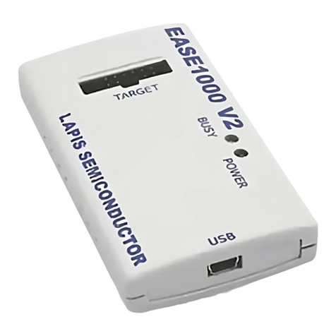
Rohm Lapis EASE1000 V2 User manual

Rohm

Rohm Lapis EASE1000 V2 User manual

Rohm RKX-EVK-001 User manual

Rohm

Rohm RKX-EVK-001 User manual

Rohm LAPIS RB-S22660GD32 User manual

Rohm

Rohm LAPIS RB-S22660GD32 User manual

Rohm LAPIS SEMICONDUCTOR ML620Q503 User manual

Rohm

Rohm LAPIS SEMICONDUCTOR ML620Q503 User manual

Rohm BD91N01NUX Installation and operating instructions

Rohm

Rohm BD91N01NUX Installation and operating instructions

Rohm LAPIS Technology RB-D610Q339TB64 User manual

Rohm

Rohm LAPIS Technology RB-D610Q339TB64 User manual

Rohm LAPIS Semiconductor ML620Q151B User manual

Rohm

Rohm LAPIS Semiconductor ML620Q151B User manual

Popular Microcontroller manuals by other brands

Freescale Semiconductor MPC5634M manual

Freescale Semiconductor

Freescale Semiconductor MPC5634M manual

Microchip Technology PIC16F87XA datasheet

Microchip Technology

Microchip Technology PIC16F87XA datasheet

GigaDevice Semiconductor GD32F403 Series user manual

GigaDevice Semiconductor

GigaDevice Semiconductor GD32F403 Series user manual

Microchip Technology EVB-LAN9254-DIGIO user guide

Microchip Technology

Microchip Technology EVB-LAN9254-DIGIO user guide

GlobalScale MiraBox user guide

GlobalScale

GlobalScale MiraBox user guide

Cytron Technologies CIKU user manual

Cytron Technologies

Cytron Technologies CIKU user manual

ST STM32F2 Series user manual

ST

ST STM32F2 Series user manual

Velleman KA01 manual

Velleman

Velleman KA01 manual

Intrinsyc Open-Q 2500 user guide

Intrinsyc

Intrinsyc Open-Q 2500 user guide

NEC mPD789026 Subseries user manual

NEC

NEC mPD789026 Subseries user manual

Intel Stratix 10 GX user guide

Intel

Intel Stratix 10 GX user guide

ST ST25R3911B-DISCO user manual

ST

ST ST25R3911B-DISCO user manual

Microchip Technology PIC32MZ user guide

Microchip Technology

Microchip Technology PIC32MZ user guide

Congatec conga-SKIT quick start guide

Congatec

Congatec conga-SKIT quick start guide

Texas Instruments CC2540 quick start guide

Texas Instruments

Texas Instruments CC2540 quick start guide

Nvidia JETSON TX1 Quick start guides

Nvidia

Nvidia JETSON TX1 Quick start guides

NXP Semiconductors MC9S08QL8 MCU Series Reference manual

NXP Semiconductors

NXP Semiconductors MC9S08QL8 MCU Series Reference manual

NEC mPD17120 Subseries user manual

NEC

NEC mPD17120 Subseries user manual

manuals.online logo
manuals.online logoBrands
  • About & Mission
  • Contact us
  • Privacy Policy
  • Terms and Conditions

Copyright 2025 Manuals.Online. All Rights Reserved.