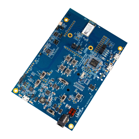
Rohm LAPIS RB-S22660GD32 User manual

FEBL22660GDRB-02
RB-S22660GD32
User's Manual
Issue Date: February 5, 2021

RB-S22660GD32
User’s Manual
FEBL22660RB
I
Notes
1) The information contained herein is subject to change without notice.
2) When using LAPIS Technology Products, refer to the latest roduct information (data sheets, user’s manuals, a lication
notes, etc.), and ensure that usage conditions (absolute maximum ratings, recommended o erating conditions, etc.) are within
the ranges s ecified. LAPIS Technology disclaims any and all liability for any malfunctions, failure or accident arising out
of or in connection with the use of LAPIS Technology Products outside of such usage conditions s ecified ranges, or without
observing recautions.
Even if it is used within such usage conditions s ecified ranges, semiconductors can break down and
malfunction due to various factors.
Therefore, in order to revent ersonal injury, fire or the other damage from break down
or malfunction of LAPIS Technology Products, lease take safety at your own risk measures such as com lying with the
derating characteristics, im lementing redundant and fire revention designs, and utilizing backu s and fail-safe rocedures.
You are res onsible for evaluating the safety of the final roducts or systems manufactured by you.
3) Descri tions of circuits, software and other related information in this document are rovided only to illustrate the standard
o eration of semiconductor roducts and a lication exam les.
You are fully res onsible for the incor oration or any other
use of the circuits, software, and information in the design of your roduct or system.
And the eri heral conditions must be
taken into account when designing circuits for mass roduction.
LAPIS Technology disclaims any and all liability for any
losses and damages incurred by you or third arties arising from the use of these circuits, software, and other related
information.
4) No license, ex ressly or im lied, is granted hereby under any intellectual ro erty rights or other rights of LAPIS Technology
or any third arty with res ect to LAPIS Technology Products or the information contained in this document (including but
not limited to, the Product data, drawings, charts, rograms, algorithms, and a lication exam les、etc.). Therefore LAPIS
Technology shall have no res onsibility whatsoever for any dis ute, concerning such rights owned by third arties, arising
out of the use of such technical information.
5) The Products are intended for use in general electronic equi ment (AV/OA devices, communication, consumer systems,
gaming/entertainment sets, etc.) as well as the a lications indicated in this document.
For use of our Products in a lications
requiring a high degree of reliability (as exem lified below), lease be sure to contact a LAPIS Technology re resentative
and must obtain written agreement: trans ortation equi ment (cars, shi s, trains, etc.), rimary communication equi ment,
traffic lights, fire/crime revention, safety equi ment, medical systems, servers, solar cells, and ower transmission systems,
etc.
LAPIS Technology disclaims any and all liability for any losses and damages incurred by you or third arties arising by
using the Product for ur oses not intended by us. Do not use our Products in a lications requiring extremely high reliability,
such as aeros ace equi ment, nuclear ower control systems, and submarine re eaters, etc.
6) The Products s ecified in this document are not designed to be radiation tolerant.
7) LAPIS Technology has used reasonable care to ensure the accuracy of the information contained in this document. However,
LAPIS Technology does not warrant that such information is error-free and LAPIS Technology shall have no res onsibility
for any damages arising from any inaccuracy or mis rint of such information.
8) Please use the Products in accordance with any a licable environmental laws and regulations, such as the RoHS Directive.
LAPIS Technology shall have no res onsibility for any damages or losses resulting non-com liance with any a licable laws
or regulations.
9) When roviding our Products and technologies contained in this document to other countries, you must abide by the
rocedures and rovisions sti ulated in all a licable ex ort laws and regulations, including without limitation the US Ex ort
Administration Regulations and the Foreign Exchange and Foreign Trade Act..
10) Please contact a ROHM sales office if you have any questions regarding the information contained in this document or LAPIS
Technology's Products.
11) This document, in art or in whole, may not be re rinted or re roduced without rior consent of LAPIS Technology.
(Note) “LAPIS Technology” as used in this document means LAPIS Technology Co., Ltd.
Copyright 2020 – 2021 LAPIS Technology Co., Ltd.
2-4-8 Shinyokohama, Kouhoku-ku, Yokohama 222-8575, Japan
https://www.lapis-tech.com/en/
RB-S22660GD32 User’s Manual
FEBL22660GDRB i
Table of Contents
1. Overview.............................................................................................................................................................1
2. Operational notes...............................................................................................................................................1
3. Specification .......................................................................................................................................................2
3.1. EROFF jumper pin.....................................................................................................................................2
3.2. OE jumper pin ............................................................................................................................................2
3.3. IOVDD jumper pin .....................................................................................................................................2
3.4. OUT jumper pin .........................................................................................................................................2
3.5. LOUT jack...................................................................................................................................................2
3.6. SP jack.........................................................................................................................................................3
3.7. AIN through hall ........................................................................................................................................3
3.8. SPVDD jumper terminal, EXT through hall ............................................................................................3
3.9. SAD2-0 lands ..............................................................................................................................................3
3.10. XT1 land, J1 land .......................................................................................................................................4
3.11. CN1 connector ............................................................................................................................................4
3.12. CN2 connector ............................................................................................................................................5
4. Appendix.............................................................................................................................................................6
4.1. PCB layout..................................................................................................................................................6
4.2. BOM list, Schematic ..................................................................................................................................7
5. Revision History.................................................................................................................................................9

RB-S22660GD32 User’s Manual
FEBL22660GDRB 1
1. Overview
This instruction manual is for the RB-S22660GD32 which is reference board for the ML22660 (hereinafter referred to as
"Speech Synthesis LSIs").
This board can be combined with Sound Device Control Board 3 (hereinafter referred to as "SDCB3") to do the following:
-Voice playback by ML22660.
-Writing sound code data into serial FLASH memory.
By connecting a flash writer to the RB-S22660GD32, sound code data can be written to the serial flash memory.
2. Operational notes
The following describes the precautions to follow when handling the RB-S22660GD32.
-Turn off the power when attaching the RB-S22660GD32 to the SDCB3.
-Turn off the power when loading Speech Synthesis LSIs into the RB-S22660GD32. Pin 1 is the position of the board
silk ▲at the bottom left with respect to the socket opening. The Figure 1 shows the setting directions of Speech
Synthesis LSIs.
-The ML22660 supply voltages are 2.7 to 3.6V / 3.3 to 5.5V. Use the RB-S22660GD32 with a power supply voltage of
3.0V.
-Connect LOUT jack and SP jack to the mono speaker.
-RB-S22660GD32 is a device used only by experts in R&D facilities for research and development purposes.
RB-S22660GD32 is not intended to be used in mass-produced products or parts thereof.
-The information in this document is subject to change without notice due to product improvement and technological
improvement. Prior to use, please ensure that the information is up to date.
-LAPIS Technology does not provide any RB-S22660GD32 support. Replace only in case of initial failure.
-
Figure 1 Outline Diagram

RB-S22660GD32 User’s Manual
FEBL22660GDRB 2
3. Specification
3.1. EROFF jumper pin
EROFF jumper pin is jumper pin that switch the connection of EROFF pin of Speech Synthesis LSIs.
EROFF
Contents
NML
EROFF pin is connected to CN1,CN2.
PRG
EROFF pin is connected to IOVDD.
Set to NML when connecting to SDCB3 for use. EROFF pin is controlled from SDCB3.
When this board is used by itself, setting PRG enables the serial flash memory interface of Speech Synthesis LSIs.
3.2. OE jumper pin
OE jumper pin is a jumper pin that enables or disables the signal input/output of CN1 pins to the serial flash memory pins.
OE
Contents
NML
Enable: The pins of the serial flash memory are input/output from the pins of CN1.
PRG
Disable: The pins of the serial flash memory do not input/output from the pins of CN1.
Set to NML when connecting to SDCB3 for use.
When this board is used by itself, the serial flash memory interface signal of Speech Synthesis LSIs and CN2 signal are
input/output to the serial flash memory when OE jumper pin is set to PRG.
3.3. IOVDD jumper pin
IOVDD jumper pin is jumper pin that switch the connection of IOVDD pin of Speech Synthesis LSIs.
IOVDD
Contents
SDCB3
IOVDD pin is connected to the output (3.0V) of the LDO mounted on this board.
CN2
IOVDD pin is connected to 23pin of CN2.
Set to SDCB3 when connecting to SDCB3 for use.
When this board is used by itself, power can be supplied to IOVDD terminal of the speech synthesis LSI from 23pin of
CN2 when IOVDD jumper pin is set to CN2.
3.4. OUT jumper pin
OUT jumper pin is jumper pin that switch the connection of SPP pin of Speech Synthesis LSIs.
OUT
Contents
LOUT
SPP pin is connected to LOUT jack.
SP
SPP pin is connected to SP jack.
3.5. LOUT jack
LOUT jack is a jack where the signal from LOUT pins of Speech Synthesis LSIs is output via the speaker amplifier.
Set Mode of Play setting of SDCB Controller to Line AMP(SPP). (Refer to Speech LSI Utility User's Manual.)
Connect a monaural speaker.

RB-S22660GD32 User’s Manual
FEBL22660GDRB 3
3.6. SP jack
SP jack is a jack where the signal from SPP,SPM pins of Speech Synthesis LSIs is output.
Set Mode of Play setting of SDCB Controller to Speaker AMP. (Refer to Speech LSI Utility User's Manual.)
Connect a monaural speaker.
3.7. AIN through hall
AIN through hole is used to input signals from an external source to the AIN pin of Speech Synthesis LSIs.
Input the speaker amplifier input signal to AIN through hole.
Figure 2 AIN through hall
3.8. SPVDD jumper terminal, EXT through hall
SPVDD jumper terminal is used to switch the destination of SPVDD pins of Speech Synthesis LSIs.
When supplying from SDCB3, connect 1-2pin of SPVDD jumper terminal.
To supply from an external source, cut the pattern between 1 and 2 pins of SPVDD jumper terminal and input SPVDD from
the EXT throughhole.
Figure 3 SPVDD jumper terminal
3.9. SAD2-0 lands
SAD2-0 lands are used to change SAD2-0 setting of Speech Synthesis LSIs.
This board is shipped to DVDD (I2C slave address is 111_101).
When connecting this board to SDCB3 and using it, set DVDD to the factory default settings.
To set any I2C slave address, change the connection of SAD2-0 lands.
Cut this when cutting the 1-2-pin
pattern of SPVDD jumper terminal.
Speech Synthesis LSIs

RB-S22660GD32 User’s Manual
FEBL22660GDRB 4
Figure 4 SAD2-0 lands
3.10. XT1 land, J1 land
XT1 land is used to mount the Ceramic resonator.
When using a ceramic resonator for the clock of Speech Synthesis LSIs, mount the components.
When no component is mounted, Speech Synthesis LSIs operates with built-in RC oscillation.
Figure 5 Ceramic resonator
A typical example of a ceramic resonator that matches XT1 land foot pattern is shown below.
Vendor
Frequency[Hz]
Parts Number
Murata Manufacturing Co., Ltd.
4M
CSTCR4M00G55B-R0
Murata Manufacturing Co., Ltd. 4.096M CSTCR4M09G55B-R0
J1 land is land connecting the XT pin of speech synthesis LSIs to the 28pin (XT) of CN2.
To use an external clock for Speech Synthesis LSIs clock, connect the pins of the J1 land and input them from the 28pin
(XT) of CN2.
Figure 6 J1 land
3.11. CN1 connector
CN1 connector is used to connect to SDCB3.
Change DVDD or GND to the desired
I2C slave address.
ceramic resonator
Connect the terminals of the J1 lands.

RB-S22660GD32 User’s Manual
FEBL22660GDRB 5
3.12. CN2 connector
CN2 connector is used to connect to the pins of Speech Synthesis LSIs.
CN2
Pin No
LSI
I/O
Pin No Pin Name
SDCB3
connection
Single unit
serial flash memory interface:
Enable
Single unit
serial flash memory interface:
Disable
1
19
DVDD *1
O
I
I
2
19
DVDD *1
O
I
I
3 28 RESETB O I I
4 29 TEST0 O I I
5 30 STATUS1 O O O
6 31 STATUS2 O O O
7 32 CBUSYB O O O
8 - - - - -
9 4 SCL O I I
10 5 SDA O I/O I/O
11 - - - - -
12 10 ERSCK
*4
O I I
13 12 ERSO
*4
O I I
14 11 ERSI O O O
15 1, 18 DGND - - -
16 1, 18 DGND - - -
17 9 ERCSB O O I
18 10 ERSCK O O I
19 11 ERSI O O O
20
12
ERSO
O
O
I
21
13
EROFF
O
O
I
22
-
-
-
-
-
23 14 IOVDD
*1,3
O I I
24 - - - - -
25 1, 18 DGND - - -
26 1, 18 DGND - - -
27 16 XTB
*2
O O O
28 17 XT
*2
O I I
29 1, 18 DGND - - -
30 1, 18 DGND - - -
*1 Do not supply DVDD,IOVDD from CN2 when connecting SDCB3.
*2 When the J1 and J2 lands are connected, the XT and XTB pins of Speech Synthesis LSIs are input and output.
*3 Supply IOVDD externally when IOVDD jumper pin is set to CN2.
*4 When IOVDD jumper pin is set to SDCB3, this pin is not connected to the terminal of the speech synthesis LSI. When
IOVDD jumper pin is set to CN2, this pin is connected to the pin of the speech synthesis LSI.
Figure 7 CN2 connectors hole pattern

RB-S22660GD32 User’s Manual
FEBL22660GDRB 7
4.2. BOM list, Schematic
Parts Number Symbol Contents Qty. Vendor
1 QTU-11896 RB-S22660GD32 PCB 1 LAPIS Technology Co., Ltd.
2 CGA3E2X7R1E104K080AA
C1,C3,C4,C5,
C7,C11,C13,C14,
C15,C18
Ceramic Capacitor
0.1μF/25V X7R 10 TDK Corporation
3 CGA3E1X7R1C474M080AC C16,C17
Ceramic Capacitor
0.47μF/16V X7R
2 TDK Corporation
4 CGA3E1X7R1C105K080AC C2,C6,C10
Ceramic Capacitor
1.0μF/16V X7R
3 TDK Corporation
5 C1608X5R1C335K080AC C8,C12
Ceramic Capacitor
3.3μF/16V X5R
2 TDK Corporation
6 HIF3FB-40DA-2.54DSA(71) CN1 40pin Receptacle 1 Hirose Electric Co., Ltd.
7 A2-3PA-2.54DSA EROFF,OUT,IOVDD,OE 3pin Pin Header 4 Hirose Electric Co., Ltd.
8 MJ-354A0 JACK1,JACK2
2-Conductor Miniature
Jack
2
MARUSHIN ELECTRIC MFG.
CO., LTD.
9 MCR03EZPJ203 R1 Resistor 20kΩ ±5% 1 Rohm Co., Ltd.
10 MCR03EZPJ103 R2 Resistor 10kΩ ±5% 1 Rohm Co., Ltd.
11 MCR03EZPJ104 R3,R4 Resistor 100kΩ ±5% 2 Rohm Co., Ltd.
12 - SAD0,SAD1,SAD2 Select pad 3 -
13 IC610-0324-007 U1 QFN P0.50 32P Socket 1
YAMAICHI ELECTRONICS
Co., Ltd.
14 LM4890MM/NOPB U2 Audio Power Amplifier 1
Texas Instruments
Incorporated
15 TXS0108EPWR U3 Voltage level translation 1
Texas Instruments
Incorporated
16 MT25QL128ABA1ESE U4
128Mb Serial NOR Flash
Memory
1 Micron Technology, Inc.
17 BU30SD2MG-MTR U5 LDO Regulator 1 Rohm Co., Ltd.
18 TC7SH125FU U6
Bus Buffer with 3-State
Output
1 Toshiba Corporation
19 HIF3GA-2.54SP - Short Pin 4 Hirose Electric Co., Ltd.
20 - CN2 Unmounted 1 -
21 - J1,J2,J3,J4,J5,J6 Unmounted 6 -
22 - SPVDD Unmounted 1 -
23 - TH1,TH2,TH3,TH4 Unmounted 4 -
24 - XT1 Unmounted 1 -

RB-S22660GD32 User’s Manual
FEBL22660GDRB 8
LAPIS Technology Co., Ltd.

RB-S22660GD32 User’s Manual
FEBL22660GDRB 9
5. Revision History
Document No. Issue Date
Page
Description
Previous
Edition
New
Edition
FEBL22660RGDB-01
March 9,
2020
–
–
First edition.
FEBL22660GDRB-02
February 5
2021
Notes
Notes
Change the description.
Company name change.
1
1
2. Operational notes
Added to connect a monaural speaker to the
LOUT jack and SP jack.
-
2
3.1. EROFF jumper pin
Added chapter.
3.2. OE jumper pin
Added chapter.
3.3. IOVDD jumper pin
Added chapter.
3.4. OUT jumper pin
Added chapter.
3.5. LOUT jack
Changed chapter number.
Added SDCB Controller settings when using
LOUT jack.
Added to connect a monaural speaker to the
LOUT jack.
-
3
3.6. SP jack
Changed chapter number.
Added SDCB Controller settings when using
SP jack.
Added to connect a monaural speaker to the
LOUT jack.
3.7. AIN through hall
Changed chapter number.
Changed chapter name.
Added connection diagram.
3.8, SPVDD jumper terminal, EXT through hall
Added chapter.
3.9, SAD2-0 lands
Added chapter.
-
4
3.10. XT1 land, J1 land
Changed chapter number.
Changed chapter name.
Added operation in RC oscillation.
3.11. CN1 connector
Changed chapter number.
-
5
3.12. CN2 connector
Changed chapter number.
Added input/output directions when SDCB3 is
connected and single unit is used.
-
6
4. Appendix
Added chapter.
Table of contents
Other Rohm Microcontroller manuals

Rohm
Rohm LAPIS Technology RB-D610Q339TB64 User manual

Rohm
Rohm RKX-EVK-001 User manual

Rohm
Rohm LAPIS SEMICONDUCTOR ML620Q503 User manual

Rohm
Rohm BD91N01NUX Installation and operating instructions

Rohm
Rohm LAPIS ML610Q305 User manual

Rohm
Rohm LAPIS Semiconductor ML620Q151B User manual

Rohm
Rohm Lapis EASE1000 V2 User manual
Popular Microcontroller manuals by other brands

Dialog Semiconductor
Dialog Semiconductor DA14681 Quick starting guide

M5Stack
M5Stack PICO quick start guide

Basler
Basler Add-on Camera Kit Quick install guide

NXP Semiconductors
NXP Semiconductors MPC5566 Reference manual

HETRONIC
HETRONIC ERGO-S Service manual

Nordic Semiconductor
Nordic Semiconductor Power Profiler Kit user guide