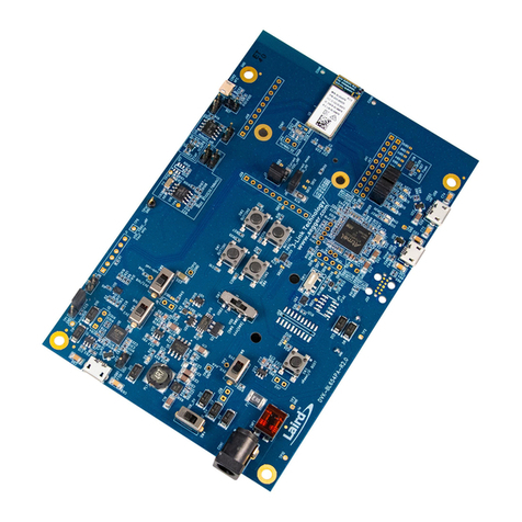
Rohm LAPIS Technology RB-D610Q339TB64 User manual

FEBL610Q339RB-01
RB-D610Q339TB64
User's Manual
Issue Date: January 13, 2022

RB-D610Q339TB64 User’s Manual
FEBL610Q339RB i
Notes
1) The information contained herein is subject to change without notice.
2) When using LAPIS Technology Products, refer to the latest product information (data sheets, user’s manuals, application
notes, etc.), and ensure that usage conditions (absolute maximum ratings, recommended operating conditions, etc.) are within
the ranges specified. LAPIS Technology disclaims any and all liability for any malfunctions, failure or accident arising out
of or in connection with the use of LAPIS Technology Products outside of such usage conditions specified ranges, or without
observing precautions. Even if it is used within such usage conditions specified ranges, semiconductors can break down and
malfunction due to various factors. Therefore, in order to prevent personal injury, fire or the other damage from break down
or malfunction of LAPIS Technology Products, please take safety at your own risk measures such as complying with the
derating characteristics, implementing redundant and fire prevention designs, and utilizing backups and fail-safe procedures.
You are responsible for evaluating the safety of the final products or systems manufactured by you.
3) Descriptions of circuits, software and other related information in this document are provided only to illustrate the standard
operation of semiconductor products and application examples. You are fully responsible for the incorporation or any other
use of the circuits, software, and information in the design of your product or system. And the peripheral conditions must be
taken into account when designing circuits for mass production. LAPIS Technology disclaims any and all liability for any
losses and damages incurred by you or third parties arising from the use of these circuits, software, and other related
information.
4) No license, expressly or implied, is granted hereby under any intellectual property rights or other rights of LAPIS Technology
or any third party with respect to LAPIS Technology Products or the information contained in this document (including but
not limited to, the Product data, drawings, charts, programs, algorithms, and application examples、etc.). Therefore LAPIS
Technology shall have no responsibility whatsoever for any dispute, concerning such rights owned by third parties, arising
out of the use of such technical information.
5) The Products are intended for use in general electronic equipment (AV/OA devices, communication, consumer systems,
gaming/entertainment sets, etc.) as well as the applications indicated in this document. For use of our Products in applications
requiring a high degree of reliability (as exemplified below), please be sure to contact a LAPIS Technology representative
and must obtain written agreement: transportation equipment (cars, ships, trains, etc.), primary communication equipment,
traffic lights, fire/crime prevention, safety equipment, medical systems, servers, solar cells, and power transmission systems,
etc. LAPIS Technology disclaims any and all liability for any losses and damages incurred by you or third parties arising by
using the Product for purposes not intended by us. Do not use our Products in applications requiring extremely high reliability,
such as aerospace equipment, nuclear power control systems, and submarine repeaters, etc.
6) The Products specified in this document are not designed to be radiation tolerant.
7) LAPIS Technology has used reasonable care to ensure the accuracy of the information contained in this document. However,
LAPIS Technology does not warrant that such information is error-free and LAPIS Technology shall have no responsibility
for any damages arising from any inaccuracy or misprint of such information.
8) Please use the Products in accordance with any applicable environmental laws and regulations, such as the RoHS Directive.
LAPIS Technology shall have no responsibility for any damages or losses resulting non-compliance with any applicable laws
or regulations.
9) When providing our Products and technologies contained in this document to other countries, you must abide by the
procedures and provisions stipulated in all applicable export laws and regulations, including without limitation the US Export
Administration Regulations and the Foreign Exchange and Foreign Trade Act.
10) Please contact a ROHM sales office if you have any questions regarding the information contained in this document or LAPIS
Technology's Products.
11) This document, in part or in whole, may not be reprinted or reproduced without prior consent of LAPIS Technology.
(Note) “LAPIS Technology” as used in this document means LAPIS Technology Co., Ltd.
Copyright 2022 LAPIS Technology Co., Ltd.
2-4-8 Shinyokohama, Kouhoku-ku, Yokohama 222-8575, Japan
https://www.lapis-tech.com/en/
RB-D610Q339TB64 User’s Manual
FEBL610Q339RB ii
Table of Contents
1. Overview.............................................................................................................................................................1
2. Operational notes...............................................................................................................................................1
3. Hardware specifications ....................................................................................................................................1
4. Board Outline Diagram .....................................................................................................................................2
5. Specification .......................................................................................................................................................2
5.1. Power Circuit..............................................................................................................................................2
5.2. LED(P22-P24).............................................................................................................................................3
5.3. ADC(AIN4-AIN7) .......................................................................................................................................4
5.4. Jack .............................................................................................................................................................4
5.5. CN1 Connector ...........................................................................................................................................5
5.6. CN2 Connector ...........................................................................................................................................6
5.7. CNE connector............................................................................................................................................6
6. PCB specification, BOM list and Schematic ....................................................................................................7
6.1. PCB specification .......................................................................................................................................7
6.2. BOM list......................................................................................................................................................8
6.3. Schematic....................................................................................................................................................8
7. Revision History.............................................................................................................................................. 10

RB-D610Q339TB64 User’s Manual
FEBL610Q339RB 1
1. Overview
This instruction manual is for the RB-D610Q339TB64 which is the reference board for ML610Q339 (hereinafter referred to
as "MCU") that is 8-bit microcontroller with voice output function.
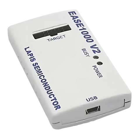
This board can be combined with on-chip debug tool EASE1000 V2 and software development enviroment(DUT8 and
MWU16) to do the following:
-Development and debugging of the MCU control software.
-Programing control and sound code data to the MCU internal Flash-ROM.
-Voice playback by the MCU.
2. Operational notes
The following describes the precautions to follow when handling the RB-D610Q339TB64.
-Turn off the power when inserting and removing jumper socket from PWR/VREF /SPVDD Jumper pin on the RB-
D610Q339TB64.
-Turn off the power when attaching and deattaching external board, device and cable from CN1/CN2/CNE Connector on
the RB-D610Q339TB64.
-Connect only monaural speakers to the jack on the RB-D610Q339TB64.
-RB-D610Q339TB64 is a device used only by experts in R&D facilities for research and development purposes. RB-
D610Q339TB64 is not intended to be used in mass-produced products or parts thereof.
-The information in this document is subject to change without notice due to product improvement and technological
improvement. Prior to use, please ensure that the information is up to date.
-LAPIS Technology does not provide any RB-D610Q339TB64 support. Replace only in case of initial failure.
3. Hardware specifications
Table 1 shows the hardware specifications of RB-D610Q339TB64. For more information about the connection of the mounted
components, see the schematic.
Table 1 Hardware specifications
Mounted LSI
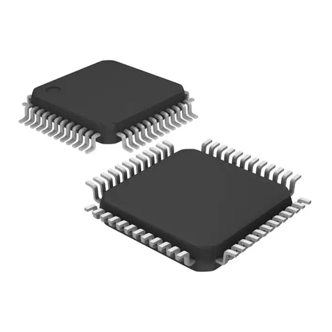
・U1: ML610Q339 64pin TQFP
Other Mounted
components
・PWR(J1): Jumper for selecting the power supply input (3pin pin-header and short pin)
・VREF(J2): Jumper for selecting VREF(3pin pin-header and short pin)
・SPVDD(J3): Jumper for selecting SPVDD(3pin pin-header and short pin)
・C1-C4: Capacitors for Powers
・P22-P24: LEDs
・R1-R3: Resistors for LEDs
・R4-R6: Jumper Chip for connecting LEDs
・ R7-R10: Resistors for Successive Approximation Type A-D Converter
・JACK: Jack for connecting Speakers
・CNE: Connector for EASE1000 V2(14pin connector)
Pads (or/and)
Through holes for
mounting components
・C5-C8: Capacitors for Successive Approximation Type A-D Converter
・CN1-CN2: Connectors for user application system (32pin, 2.54mm pitch, φ0.8mm )
・SP1: Land for ferrite beads(1608)
Power check pins/pads
・VDD、SPVDD、UVDD、USPVDD、VSS、SPVSS、AIN4-AIN7 (φ0.8mm)
Operating voltage
・+2.0~+5.5V
Board size
・55.88 mm x 93.98 mm

RB-D610Q339TB64 User’s Manual
FEBL610Q339RB 2
4. Board Outline Diagram
Figure 1 shows an outline diagram of the RB-D610Q339TB64.
Figure 1 Board Outline Diagram
5. Specification
5.1. Power Circuit
Figure 2 shows a power curcuit of the RB-D610Q339TB64.The RB-D610Q339TB64 has junper pins that can switch the
supply source of the VDD / VREF / SPVDD pins of MCU. Each is explained below.
Figure 2 Power circuit
SPVDD
VSS
SPGND
VREF
VDD
ML610Q339
VDDL
USPVDD
UVREF
UVDD
3.3VOUT
VREF
VSS
SPVSS
VSS
SPVSS
VSS
SPVSS
VSS
VSS
SPVDD
VDD
PWR
SPVDD
VREF
CN2
CNE
VSS
VSS
USPVDD
UVDD
SPVSS
SPVSS
CNE
USR
C
VDD
USR
C
VDD
USR
C
J1
J3
J2
CN2
CNE
CN1
ADC
MCU
LED
Jumper Pin
Jack

RB-D610Q339TB64 User’s Manual
FEBL610Q339RB 3
・PWR jumper pin(J1)
PWR jumper pin can switch the supply source of VDD pin of MCU.
PWR
Contents
CNE
VDD pin is connected to 13pin of CNE.
USR
VDD pin is connected to 9pin (UVDD) of CN2.
When attaching “EASE1000 V2” on the board, PWR jumper pin set to “EASE” if power supply from 13pin of CNE connector.
PWR jumper pin set to “USR” if power supply from CN1 connector.
・VREF jumper pin(J2)
VREF jumper pin can switch the supply source of VREF pin of MCU.
VREF
Contents
VDD
VREF pin is connected to 2pin of PWR jumper pin.
USR
VREF pin is connected to 19pin (UVREF) of CN2.
VREF jumper pin set to “VDD” if power supply from VDD as same as selecting PWR jumper pin.
VREF jumper pin set to “USR” if power supply from CN2 connector.
・SPVDD jumper pin(J3)
SPVDD jumper pin can switch the supply source of SPVDD pin of MCU.
SPVDD
Contents
VDD
SPVDD pin is connected to 2pin of PWR jumper pin.
USR
SPVDD pin is connected to 3/4pins (USPVDD) of CN2.
SPVDD jumper pin set to “VDD” if power supply from VDD as same as selecting PWR jumper pin.
SPVDD jumper pin set to “USR” if power supply from CN1 connector.
5.2. LED(P22-P24)
P22-24 pins of MCU on the RB-D610Q339TB64 allow direct LEDs drive. Enable to use LEDs connecting these pins when
the N-channel open drain output is selected. Unmount register on the board indicated by “R4-R6” when not using LEDs.
Figure 3 shows the LED circuit processing example.
Figure 3 LED circuit processing example
Register

RB-D610Q339TB64 User’s Manual
FEBL610Q339RB 4
5.3. ADC(AIN4-AIN7)
The RB-D610Q339TB64 has registers indicated by "R7-R10" and capacitors indicated by "C5-C8" (not mounted) so that
P44-P47 pins of MCU are enable to use as AIN4-AIN7 which are Succesive Approximation type A-D Converter functions.
Mount a noise reduciton capacitor on board land indicated by “C5-C8”if necessary. Figure 4 shows the ADC circuit
processing example.
When using the Succesive Approximation type A-D Converter functions without using resistors, apply a voltage to the through
hole.
Figure 4 ADC circuit processing example
5.4. Jack
Jack is connnected to SPP/SPM pins of the MCU.
Connect only monaural speakers to the jack.
Through hole for
applying voltage
Land size of 1608 for
mounting capacitor

RB-D610Q339TB64 User’s Manual
FEBL610Q339RB 5
5.5. CN1 Connector
The through holes indicated by “CN1” are enable to mount connector that specification is double row, 16 positions and
2.54mm(0.1mil) pich.
Table 2 shows a CN1 connector pin assignment.
Table 2 CN1 connector pin assignment
CN1
Connected to
Remarks
Pin number
Part Symbol
Number
Pin name
1
U1
1
P93
2
U1
2
P94
3
U1
3
P80/EXI0
4
U1
4
P81/EXI1
5
U1
5
P20/LED0
6
U1
6
P21/LED1
7
U1
7
P22/LED2
8
VSS
-
VSS
9
U1
9
P23/LED3
10
U1
10
P24/LED4
11
U1
11
P25/LED5
12
U1
12
P91
13
U1
13
P95
14
U1
14
P96
15
VSS
-
VSS
16
VSS
-
VSS
17
U1
17
PA7
18
U1
18
PA6
19
U1
19
PA5
20
U1
20
PA4
21
U1
21
P82/EXI2
22
U1
22
P83/EXI3
23
U1
23
PA3
24
U1
24
PA2
25
U1
25
PA1
26
U1
26
PA0
27
U1
27
P90
28
U1
28
RESET_N
29
U1
29
SPP
30
U1
30
SPP
31
U1
31
SPM
32
U1
32
SPM

RB-D610Q339TB64 User’s Manual
FEBL610Q339RB 6
5.6. CN2 Connector
The through holes indicated by “CN2”are enable to mount connector that specification is double row, 16 positions and
2.54mm(0.1mil) pich.
Table 3 shows a CN2 connector pin assignment.
Table 3 CN2 connector pin assignment
CN2
Connected to
Remarks
Pin number
Part Symbol
Number
Pin name
1
U1
33
SPVSS
2
U1
34
SPVSS
3
J3
3
USPVDD
J3:SPVDD jumper
4
J3
3
USPVDD
J3:SPVDD jumper
5
U1
37
P84/EXI4
6
U1
38
P92
7
VSS
-
VSS
8
VSS
-
VSS
9
J1
3
UVDD
J1:PWR jumper
10
U1
42
PB0
11
U1
43
PB1/TIA0A
12
U1
44
PB2/TIA0C
13
U1
45
PB3
14
U1
46
PB4
15
U1
47
PB5
16
U1
48
PB6
17
U1
49
PC3
18
U1
50
PC2
19
J2
3
UVREF
J2:VREF jumper
20
U1
52
P40/AIN0/HPC0
21
U1
53
P41/AIN1/HPC1
22
U1
54
P42/AIN2/TIAOUT
23
U1
55
P43/AIN3
24
U1
56
P44/AIN4
25
U1
57
P45/AIN5
26
U1
58
P46/AIN6
27
U1
59
P47/AIN7
28
U1
60
P85/EXI5
29
U1
61
P86/EXI6
30
U1
62
P87/EXI7
31
U1
63
PC0
32
U1
64
PC1
5.7. CNE connector
CNE connector is used to connect the on-chip debug tool EASE1000 V2 manufactured by LAPIS Technology Co.,Ltd.
Refer to the “EASE1000 V2 User’s Manual” for details.

RB-D610Q339TB64 User’s Manual
FEBL610Q339RB 8
6.2. BOM list
Table 4 BOM list
Parts Number
Symbol
Contents
Qty.
Vendor
1
QTU-11952
RB-D610Q339TB64
PWB
1
LAPIS Technology Co., Ltd.
2
C1608X7R1E105K080AB
C1,C2,C3,C4
Ceramic Capacitor 1uF/25V X7R
4
TDK
3
-
C5,C6,C7,C8
Unmounted
4
-
4
-
CN1,CN2
Unmounted
2
-
5
HIF3FC-14PA-2.54DSA
CNE
14pin Header
1
HIROSE
6
MJ-354A0
JACK
Monaural Speaker Jack
1
MARUSHIN
7
SML-M13UT
LED1,LED2,LED3
LED Red
3
ROHM
8
MCR03EZPJ561
R1,R2,R3
Resistor 560Ω ±5%
3
ROHM
9
MCR03EZRJ000
R4,R5,R6
Resistor 0Ω
3
ROHM
10
MCR03EZPJ102
R7,R8,R9,R10
Resistor 1kΩ ±5%
4
ROHM
11
A2-3PA-2.54DSA(71)
J1,J2,J3
3pin Header
3
HIROSE
12
HIF-3GA-2.54SP
-
Jumper Socket
3
HIROSE
13
-
TP1,TP2,TP3,TP4,TP5,TP6
Unmounted
6
-
14
-
AIN4,AIN5,AIN6,AIN7
Unmounted
4
-
15
ML610Q339-NNNTB
U1
MCU
1
LAPIS Technology Co., Ltd.
16
FF013-P3555-AR791
-
Rubber leg, Push rivet
4
KOYO FASTENER
[Note]
- The diameter of through hole of CN1 and CN2 is 0.8mm.
Using CN1 and CN2, the diameter of connector pin should use the connector below 0.8mm, such as 0.5mm.
- The parts may be changed into another parts with equivalent part special quality.
6.3. Schematic
The schematic of RB-D610Q339TB64 is shown below.

RB-D610Q339TB64 User’s Manual
FEBL610Q339RB 9
1
2
3
4
5
6
7
8
A B C D E F G H I J K
1
2
3
4
5
6
7
8
A B C D E F G H I J K
SPVSS
RB-D610Q339TB64
ML610Q339 TQFP64 Referench Board
1 1 1.0
QTS-11822
(N.C.)
(N.C.)
SCLK
SDATA
(N.C.)
(N.C.)
ML610Q339
TQFP64
VSS
SPVSS
VSS
(N.C.)
DWG No.
APPLICATION
TITLE
SHEET of Rev.
LAPIS Technology Co., Ltd.
SPVDDVDD VREF3.3VOUTUVDD UVREF VDD VDDUSPVDD
VSS_C
SP1
VDD SPVDD SPVSSVSS_C
PC3
49
PC2
50
P40
52
VREF
51
P41
53
P42
54
P43
55
P44
56
P45
57
P46
58
P47
59
P85
60
P86
61
P87
62
PC0
63
PC1
64
P93
1
P94
2
P80
3
P81
4
P20
5
P21
6
P22
7
VSS
8
P23
9
P24
10
P25
11
P91
12
P95
13
P96
14
TEST1_N
15
TEST0
16
PA7 17
PA6 18
PA5 19
PA4 20
P82 21
P83 22
PA3 23
PA2 24
PA1 25
PA0 26
P90 27
RESET_N 28
SPP 29
SPP 30
SPM 31
SPM 32
SPVSS 33
SPVSS 34
SPVDD 35
SPVDD 36
P84 37
P92 38
VSS 39
VDDL 40
VDD 41
PB0 42
PB1 43
PB2 44
PB3 45
PB4 46
PB5 47
PB6 48
U1
VSS
1k
R8
VSS
VDD3.3VOUT
Unmounted
C6
VDD
3
1
2
MJ-354A0
JACK
VSS
1
30
2
3 4
5 6
7 8
9
11
13
15
17
19
21
23
27
25
29
10
28
12
14
16
18
20
22
24
26
31 32
Unmounted
CN1
VSS
USPVDDUVDD USPVDDUVREF
SPVSSVSS
UVDD VDD USPVDD SPVDD
1u
C4
Unmounted
C5
Unmounted
C7
Unmounted
C8
1
2
3
J1
1
2
3
J2
1
2
3
J3
UVDD
TP1
VDD
TP2
USPVDD
TP3
SPVDD
TP4
AIN4
AIN5
AIN6
AIN7
1k
R7
1k
R9
1k
R10
1u
C1
VSS
1uC3
VSS
VSS
TP5
SPVSS
SPVSS
TP6
1
30
2
3 4
5 6
7 8
9
11
13
15
17
19
21
23
27
25
29
10
28
12
14
16
18
20
22
24
26
31 32
Unmounted
CN2
1 2
3 4
5 6
7 8
910
11 12
13 14
CN14P
CNE
560
R1
0
R4
RED
LED1
560
R3
0
R6
RED
LED3
560
R2
0
R5
RED
LED2
1u
C2
VREF
VSS
SPVDDVREFPWR
USR USR
VDD
USR
VDD
TEST1_N
P91
P22
P21
P20
P80
P81
P95
P96
P93
P94
TEST0
P82
P83
SPP
SPM
RESET_N
PA0
PA1
PA2
PA3
PA4
PA5
PA6
PA7
P90
P84
P92
PB0
PB1
PB2
PB3
PB4
PB5
PB6
P40
P41
P42
P43
P87
P86
P44
P45
P46
P47
PC0
PC1
PC3
PC2
P44
P45
P46
P47
P44_C
P45_C
P46_C
P47_C
TEST0
TEST1_N
SP
SPM
SPP
P93 P94
P80 P81
P20 P21
P22
P23 P24
P25 P91
P95 P96
PA7 PA6
PA5 PA4
P82 P83
PA3 PA2
PA1 PA0
P90
P92
PB0
PB2
PB4
PB6
PC2
P84
PB1
PB3
PB5
PC3
P40
P41 P42
P43 P44_C
P46_CP45_C
P47_C P85
P86 P87
PC0 PC1
P23
P24
P25
P85
SPP
SPMSPM
SPP
RESET_N
CNE
P22
P22
P24
P24
P23
P23

RB-D610Q339TB64 User’s Manual
FEBL610Q339RB 10
7. Revision History
Document No.
Issue Date
Page
Description
Previous
Edition
New
Edition
FJBL610Q339RB-01
Jan 13, 2022
–
–
First edition.
Table of contents
Other Rohm Microcontroller manuals

Rohm
Rohm Lapis EASE1000 V2 User manual

Rohm
Rohm LAPIS Semiconductor ML620Q151B User manual

Rohm
Rohm LAPIS ML610Q305 User manual

Rohm
Rohm LAPIS RB-S22660GD32 User manual

Rohm
Rohm LAPIS SEMICONDUCTOR ML620Q503 User manual

Rohm
Rohm BD91N01NUX Installation and operating instructions

Rohm
Rohm RKX-EVK-001 User manual