Sanyo DC -X1000MD User manual

I
\’
.-.
““Service Manual
“,
.:
..
:,
.,
....
..;
J
‘$
,
-,
A
....>
.,*
4
.:
1
‘]
Specifications
~Note:
CD Stereo Sound
System
,,. ,
.
. .... . .. . ..
.. . . .,- ;..-
~The below mentioned specifications are mainly based on the IHF measure me- standard.
.:.:,specications based on the DIN standard or other standards.
:.”Tuner section
fl~Frequency range . . . . . . . . . FM :87.5-108 MHz
MW :522-1,611 kHz
LW :144-290 kHz
~~Cassette deck section
;Recording system ........ AC bias,4-track, stereo
~Fast forward/
rewind time . . . . . . Approx. 120 sec. (C-60)
:CD player
Channels ................ 2-channel stereo
Frequency response . . . . . . 20-20,000 Hz
1Signal to noise ratio ..... 95 dB
“; Channel separation . . . . . . 90d5 (1 kHz)
~Total harmonic
jdistortion . . . . . . . . o.~syo (1 kHz)
/Wow and flutter . . . . . . . Undetectable
‘i Note:
]The POWER switch is mounted on the secondary side. The unit is
!not disconnected from AC-power, even when switched off.
.-
:Specification subject to change without notice.
General
DC -Xl OOOMD(GERMANY)
(d. z.)
.-
. . . .
PRODUCT CODE No.
129 352 03
They can therefore not directly be compared with
Power output ............
Irc@sJts....................
ampws . . . . . . . . . . .
Power requirements .... .
Dicnensions(approx.) . . . .
R5-X1OOO remote controller
Pcrwer source . . . . . .
Dmwnsions(approx.) . . . . .
40W x2(at 8ohms, 10%distortion)
PHONO :47k ohm (5mV)
VIDEO: 47k ohms (280mV)
SPEAKERS: 8ohms
HEADPHONES: 8ohms
AC :230V, 50HZ
360 (W) x 328 (D) x 390 (H) mm
DC :3V” R6/AAISUM-3° battery x 2
63(W) x18(D)x 175(H) mm
CBoiby noise reduction manufactured under license from Dolby
Laboratories Licensing Corporation.
“i30L8Y” and the double-D symbol no are trademarks of
Dtiby Laboratories Licensing Corporation.
REFERENCE No. WM-580625
;.

+
\‘.
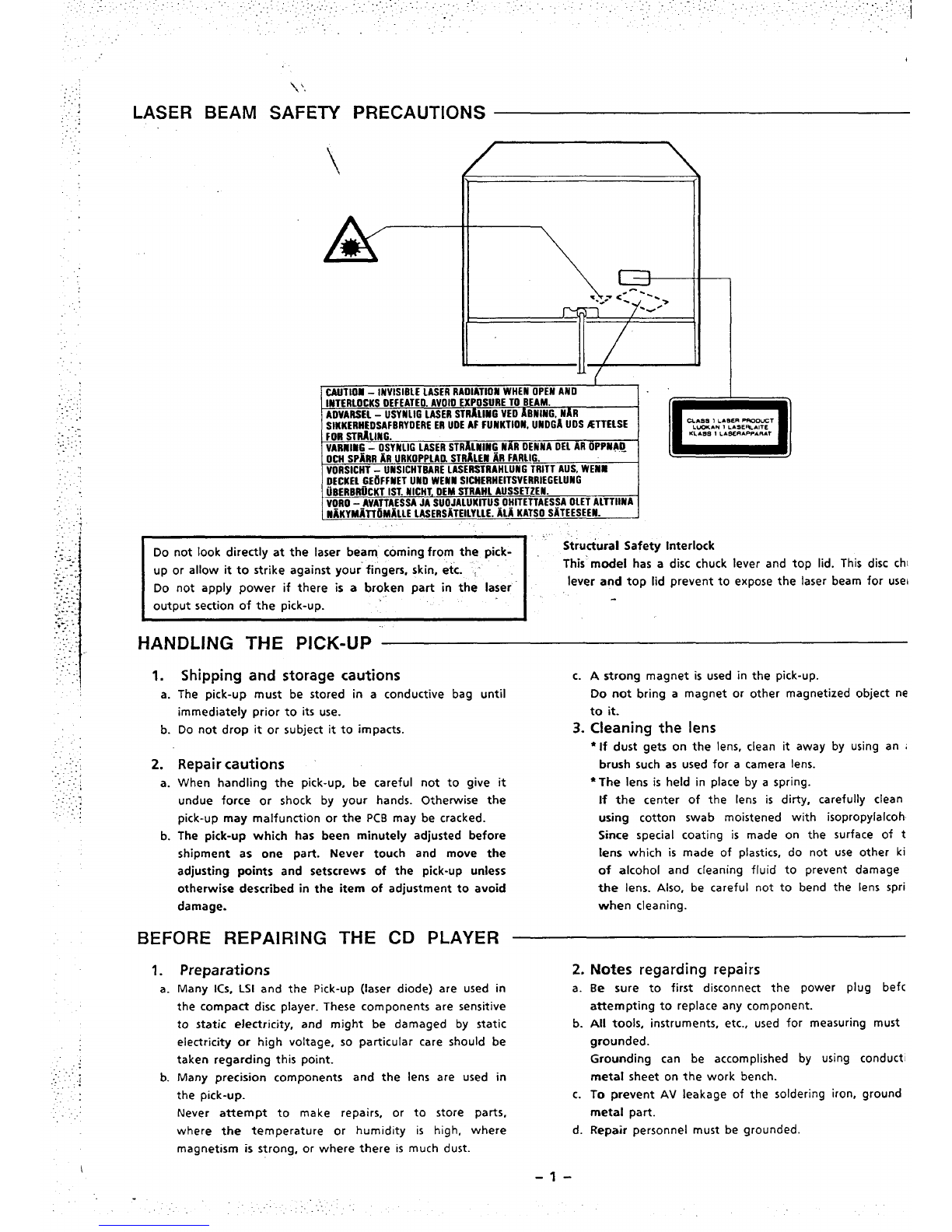
LASER BEAM SAFETY PRECAUTIONS
\I
(
CAUTION-INVISIBLELASERRADIATIONWHENOPENANO . .
INTERLOCKSOEFEATEO.AVOIOEXPOSURETOBEAM.
ADVARSE1-USYNLIGLASERSTRkLINGVEOABNING,NAR
SIKKERHEOSAFBRYOEREERUOEAFFUNKTION,UNOGAUOS)ETTELSE
:[u]
CL*96)LA8E. WOUCT
LUOK.N 1I. ASEFUAITE
FORSTtiUNG. KLAsS !LA9ERAPPA.Ar
VARNIN6-OSYNLIGLASERSTRALHINGBARoENNAoELARoF’E’N4Q
OCNSP~RRARURKOPPLAmSTRALENiiR FARLIG.
VORSICHT-UNSICHTBARELASERSTRAHLUNGTRITTAUS,WENN
DFCKE1GEhFFNETUNEIWENNSICSEERHEITSVERRIEGELUNG
---..—.
ilBERBRtiCKTIii. NtcFiT,OEMSTmiIl AUSSETZEN.
VORO-~VATTAESSAJASUOJALUKITUSOHITETTAESSAOIETALTTIINA
NAKYMATT6MhLELASERShTEILYLLE.hl~ KATSOS~TEESEEN.
~’:’”r~’afety’n
Do not look directly at the laser beam coming from the pick-
up or allow it to strike against your-fingers, skin, etc. -This’ model has adisc chuck lever and top lid. This disc ch
Do not apply power if there IS abroken part mthe laser lever and top hd prevent to expose the laser beam for usel
HANDLING THE PICK-UP
1.
a.
b.
2.
a.
b.
Shipping and storage cautions c.
The pick-up must be stored in aconductive bag until
immediately prior to its use.
Do not drop it or subject it to impacts. 3.
Repair cautions
When handling the pick-up, be careful not to give it
undue force or shock by your hands. Otherwise the
pick-up may malfunction or the PCB may be cracked.
The pick-up which has been minutely adjusted before
shipment as one part. Never touch and move the
adjusting points and setscrews of the pick-up unless
otherwise described in the item of adjustment to avoid
damage.
BEFORE REPAIRING THE CD PLAYER
1.
a.
b.
Preparations 2.
Many ICS, LSI and the Pick-up (laser diode) are used in a.
the compact disc player. These components are sensitive
to static electricity, and might be damaged by static b.
electricity or high voltage, so particular care should be
taken regarding this point.
Many precision components and the lens are used in
the pick-up. c.
Never attempt to make repairs, or to store parts,
where the temperature or humidity is high, where d.
magnetism is strong, or where there is much dust.
-1-
Astrong magnet is used in the pick-up.
Do not bring amagnet or other magnetized object ne
to it.
Cleaning the lens
‘If dust gets on the lens, clean it away by using an i
brush such as used for acamera lens.
●The lens is held in place by aspring.
If the center of the lens is dirty, carefully clean
using cotton swab moistened with isopropylalcoh
Since special coating is made on the surface of t
lens which is made of plastics, do not use other ki
of alcohol and cleaning fluid to prevent damage
the lens. Also, be careful not to bend the lens spri
when cleaning.
Notes regarding repairs
Be sure to first disconnect the power plug befc
attempting to replace any component.
All tools, instruments, etc., used for measuring must
grounded.
Grounding can be accomplished by using conduct
metal sheet on the work bench.
To prevent AV leakage of the soldering iron, ground
metal part.
Repair personnel must be grounded.

,. \’
““:DISASSEMBLY
*Switch the power OFF, and unplug the AC owercord from an
AC outlet.
:*Disassemble in the numerical sequence. \%
How to install the CD block
1.
2.
3.
4.
5.
6.
7.
Turn over the CD block so that the bottom isfacing up.
Set the gear (CM20) and bracket (CM22,23) on both sides of
the hex. shaft (CM21), and set the washer (CM17) on the
left side only.
Align the gear (CM20) with the grooves on both sides in the
rear of the loading table (CM1) and set the gear at the end
of the groove toward you.
Turn over the CD so the top is facing up, without letting the
hex. shaft, gear bracket and washer fall out.
Align the tab of the loading block base (CM2) with the
guide block (CM33) fixed at the lower left of the loading
table as shown in the figure.
After the alignment in step 5, press in the CD block slowly
and fit it into the support (CM1 5,16) as shown in the figure.
The installation will be completed after installing the
bracket (CM19) for fitting the CD block in the bottom plate
(CM14). (See cabinet exploded view)
-2-
/3!
,---
,/

\’
DISASSEMBLY
●
●
To remove the CD block, turn th idler (CM38) for loading in the
1
clockwise direction by hand sotha the CD block slides outward a
l&QJl
PINCH ROLLER
LEVER .%&
little. CM67
When installing the disc table (CM30), pull the lever (CM67) L‘G;” ~g:
i
toward you to set the (A) table on it and then release the lever. /
Applying grease and grease
1. Bottom chassis
2. Disctable
point ..-@)
.-..,enr. rl- /’:!$
--------..-—
IB
93-7 /&*
SANGROSE SG-7 y>~ I I :%D’NG “OcK ‘ASE
““W;EY
\CM16

\’
W3ASsEMi3Ly
3. Disc table (Bottom side)
0
K,;rzo //--x\--l
,-
‘C
in the spring w~ ,~/
7I%?’ ‘i”AY@!!
\
f&V~~Pick ;P portion must be
round. the maximum out
/?& SHORT I
i--if---f% I1~
ICM-K CI m= Lead wire throuah ~
‘1%
—+SAf4W&ASE
9
?-l
49
‘+1 “PINCH ROLLER
LEVER
CM67
f’-- II=
#n-k
FLOIL Q
9t.
;~ \.
OIL
..9P
k. ,1-Z -“1. Q?
LOCK LEVER
CM61
“:1 CM1
‘:.j
~’ 4. CD Mechanism block
:-i
.1 IDLER BELT
CM51
?
-“=”- “,DLERPULL=
GREASEOON?STICK
T
Y
MOUNT-M ~-.
“, AP7
CM33 \
CM44 SANGREASE SG-7
>Ia mI.)
.: DISKTRAY GEAR ?
CM53 &
4
.-”MC-GREASE EM50L
:(GEARALLAROUND)
FLOIL OIL
9L9P
Id
Inl Co -k I
IQ
-------: ”’-- yp!, J
aMi. ”nI---
(GEAR ALL Amuu,xu/ LOADING MOTOR
id?
,// L“,, ‘RACKET
&
CM32
8.9SiO.lmm
I_
/\/.
@TER:c&!JM~~~~:
:@m
marksribs~ ‘+<<~$ ‘iywR
After insert gear lever
to shaft, Lever in set
@’i
.-
Under ‘h:& Y@%,
VIEW-A
a
VIEW-B
After insert gear lever and special washer, apply MC-grease EM50L to
1/3 length portion of shaft

\’
CD ADJUSTMENT
Electrical Adjustment
So far we have presented explanat@_rs regarding compact disc
player handling. notes prior to repair,’handling the pick-up and
disassembly of the unit. Be sure to carefully read these
“:53:’’”-’
instructions before making any adjustments. BAND PA% FILTER
Preparations for Adjustments (3) Digital voltmeter (Input impedance 1Mohm or more)
Measuring instruments, tools and filter (4) Oscillator (400 Hz, 500mV RMS)
(1) Test disc.: PCD-1023 (Modern Wave H)(5) Frequency Counter (5MHz; or more)
STC-2 (Sanyo Standard Test Disc) (6) Screw drivers (non-metalic) for adjustments
(2) Oscilloscope: SS5711 (1OMHZ or dual phenomenon) (7) Band Pass Filter
or Memoryscope :DSS6521 (Storagescope) (8) AC Voltage Meter
Notes: a. The adjustments can be using the equipment produced by other manufactures provided that the performance of that
equipment corresponds to that of the above listed models.
b. Use a10:1 probe for observing signals on the oscilloscope and storage scope. .
c. Test disc is subject to change without notice.
1. Initial set ..-
Set the initial position of mechanical center position of SVF(l 1,12 as shown in figure below.
l!!!!
tCN112
u
RACKINGCAIN
SVR {1 T&T PLUG(6P)
TRACKINGBALAk4=
SVR12,
SVR11 —
I
PJ~
CN121
AM. J] )
CN161 CN151
I
Caution :II
“Power on” means at AC power plug set in the ACsocket
“Power off- means at AC power plug pull out the AC socket
these operation iscarefully to do it because possibly receive an electric shock to touch AC socket by get wet hand.
2. Free-run Frequency
1.
2.
3.
4.
5.
Adjustment (SVRI 3)
Power on.
Connect the frequency counter to TP7 (PLL) and TP4 (GND.).
TP7 place islC141-pin 18 at CD main PCB(see 36p).
Pull out the plug CN111 before adjust SVR13.
Adjust SVR13 so that the frequency counter shows
4.40 i0.1 MHz
Return the plug CN111 to original place.
*[f this adjustment is imperfect, get the long seek time, not tc
read TOC, not sound. In the worst case become high speed turn
ing reverse turning and it maywound the disc.
-5-

.;
\‘.
;CD ADJUSTMENT
~3. Tracking Balance Adjustment (SVRII)
1. Power on and press the OpenlClose key. {j
2. put on the test disc at turn table and presi. the OpenlClose key
to store the turn table.
3. Connect the oscilloscope to TP3 (TE) and TP4 (GND.).
4. power off, and in alittle while act with Power on and press the
both key PlaylClose key and Repeat key.
(Because be able to direct in the play mode. )
5. Playback the test disc with press the Play/Pause key.
6. Shift to the right end at SVR12.
7. Adjust SVR11 so that the TE (Tracking Error) signal wave-
form of TP3 on the oscilloscope is vertically symmetrical
relative to OV. (See figure right side)
8. Return the SVR12 to mechanical center.
9. power off and finish.
*If this adjustment is imperfect, become run away the sled
motor (pick-up sending motor), inferior playability.
1
II 11500LJS III
~“-4––L–-4–-4
TP1
(RF)
TP3
(TE) Ov
.. --
i4. Focus Gain Confirmation
.“:
:1. Connect the storage scope to TP2 (F.E :Focus Error) through 4. Set the output of AF oscillator to 400 Hz, 0.5V rms and connect
;the Band pass filter. (See BPF Figure) to TP5 (Focus adjust input) through resistor 120k ohms.
2. Power on the unit.
.;
,4 3. Play-back the test disc.
5. Confirm so that the voltage of the TP2 (F.E) signal waveform
on the storage scope is 0.5V p-p t3db by through BPF.
-1
‘j*[f this confirmation is imperfect, become weak the mechanical shock, inferior playability, and can not playback the Disc.
“q
-4 AF OSCILLATOR MAIN PCB OSCILLOSCOPE or STORAGESCOPE
-i
.+
i
400HZ 120K BAND PASS FILTER
~TP5
0.5V rms TP2
.: (FE)
=1I
..5. Tracking Gain Adjustment (SVRI 2)
,
1. Connect the storage scope to TP3 (T. E:Tracking Error) 4. Set the output of AF oscillator to 400 Hz, 0.5V rms and connect
through the Band pass filter. (See BPF Figure). toTP6 (Tracking adjustment input) through resistor 100k ohms.
2. Power on the unit. 5. Adjust SVR12 so that the voltage of the TP3 (T.E) signal
3. playback the test disc. waveform on the storage scope is 0.5V p-p tSo/o by
through BPF.
‘If this CONFIRMATION is imperfect, become weak the mechanical shock, inferior playability, and can not playback the Disc.
AF OSCILLATOR MAIN PCB OSCILLOSCOPE or STORAGESCOPE
.
400Hz 10OK BAND PASS FILTER
TP81
0.5V rms TP3
(TE) 1. “1 L-.
==
Don’t remove the adjusting driver for at once after adjustment of SVR.
Be sure to remove after confirm to indicate acorrect value for afew second by instructions of instrument.
-6-

\’
FLOW CHART (CD CHANGER)
Outline chart Disc table open from close Disc select from stop
Disc select
+
6
Open. Close
key in? NO
Chucking “off” mode
Come down the Base mechanism
Iw,pickupandreleasethe chucking I
I.
Vt L. IJYES
Disc “select” mode
Rotate the turn table and stop mode
with disc appoint. Reverse
+
6
620ms passed? NO
...s~-.
..3
.-1-- .,. ~......:
Z
,
c,ca>e
inished? NO
YES
Base mechanism
stopped
.
1
Chucking “on” mode F1
YES
Loading motor
high speed
Come up the Base mechanism
wlpickup and the chucking of disc.
“1’ $s:SW4 =ON
to YES
Reduction
position 4.. .. .. .
etector~ NO
i’
1I
~Discturntable Ioading section )
“t
IOpen. Close mode 1‘=’
..... Photo
. .. .. sensor input
Appli&ble . .. . .. .
number slit
etecto r?NO
Loading awhole table including--
base mechanism and able to change
the 2discsin playback. ‘“1+
-..YES
Loading motor
idling stage -r-
@
SW6=ON
to YES
Stop position
detector? NO <- .....!
Turntable
‘diin~ stage
Reverse control
SW2=ON
-7-
+
YES
Loading motor
stop stage
Reverse aloading motor when tray isclose,
and reduction position detector to by SW5.

\‘
TUNER ADJUSTMENT
.use aplastic screwdriver for adjustment.
.Adjust the intermediate frequency of A~~nd FM to the frequency of ceramic filter.
.FM tuner adjust (lF,Cover, Tracking) needn’t or It was construct by TUNER pack
RF Level: 750hm Open SG voltage dBPV
1. FM BAND Antenna :75 ohm Unblanced Direct Modulation :lkHz, t75k Hz dev.
FREQUENCY INPUT CONDITIONS OUTPUT CONDITIONS ADJUST-
STEP ITEMS INDICATED MEASURING CONNECT- MEASURING CONNECT- ING” STANDARDS
POSITION INSTRUCTIONS IONS INSTRUCTIONS IONS PARTS
IF S-Curve TP211(H) Digital
198.0 IMHz FM-SG(66dB) TP203(H)
(Ov) TP212(E) Voltmeter T2202 oio.05v
TP204(E)
FM-SG(66d8)
(Non TP211(H) Frequency
2*VCO (19 kHz) 98.0 MHz TP206(H) SVR23 19k0.05k Hz
Modulation) TP212(E) Counter TP207(E)
Standard input Modulation for Separation :Main(L+ R) :k40ki+z dev. Pilot :i6.75k Hz dev.
Note :TP204 is no earth point. Be careful so that digital voltmeter earth (including case) may not be in contact with other measuring
equipments earth. (including case) ..-
RF Level :Open SG voltage d8PV
.,
“~ 2. MW BAND Antenna :IRE Loop, Standard output: 100dB, Modulation :1 kHz 30%
..j
.i FREQUENCY
:-’1 sT’Ep INPUT CONDITIONS OUTPUT CONDITIONS ADJUST-
“,? ITEMS INDICATED MEASURING CONNECT- MEASURING CONNECT- ING STANDARDS
POSITION
“’iINSTRUCTIONS IONS INSTRUCTIONS IONS PARTS
I I I
Tuning Low 522 kHz Digital TP202(H) L2153 1.2 fo.03v ~
1--- ---
Cover High Voltmeter TP201 (E) ---. Confirm voltage
1611 kHz is below 8.OV
Low 603 kHz QTP233(H)
IRE LOOP VTVM L2152
2Tracking AM-SG @TP234(H) Max.
High 1404 kHz Ant. Oscilloscope TP235(E) CT252
3. LW BAND Antenna :IRE Loop, Standard modulation :400Hz 30%
FREQUENCY INPUT CONDITIONS OUTPUT CONDITIONS ADJUST-
STEP ITEMS INDICATED MEASURING CONNECT- MEASURING CONNECT- ING
POSITION STANDARDS
INSTRUCTIONS IONS INSTRUCTIONS IONS PARTS
Tuning Low 144 kHz Digital TP202(H) L21S4 1.6t0.05V
1--- ---
Cover High Voltmeter
290 kHz TP201 (E) --- Confirm voltage
is below 7.5v
Low 0TP233(H)
162 kHz IRE LOOP VTVM L2151
2Tracking AM-SG(85dB) @TP234(H) Max.
High 279 kHz Ant. Oscilloscope TP235(E) CT25 1
-8-

““
PARTS LOCATIONS
<TUNER>
FM+
ANT. II JI la
SVR23 1
{~
AM (E)+
ANT. (H) !CT251 CT252
@l@
lGIH
L2151 L2152
CF204 TP224(R2227)
m(v TP226(C2222)
TP203 —(0 TP205
E21a @5-Z%%TP233
L2154 L2153 TP204j T2202
6’
TP235! jTP234
ELR
A?tiUT
<DECK>
..
DECK 2
PLAYBACK
ADJUSTMENT- . .
19KHz Trap
mREC/PLAY GAIN
ADJUSTMENT EFEECT ADJUST HIGH SPEED
SVR33 SVR31 SVR30 SVR32 SVR35 SVR34 L3730 L3830 TEST POINT
Rch Lch Lch Rch Lch L7K L7K Lch Rch
%%d~~ ?; ; ,%iii!il-
Rch Lch
u
CN303
1
IC370
CN371
7
DECK 1
PLAY HEAD
CONNECTOR
DECK 2SVR37 SVR36 E-HEAD
R/P HEAD Rch Lch CONNECTOR
CONNECTOR~
BIAS ADJUSTMENT
-9-

.
jADJUSTMENT OF DECk & TORQUE
1. Amplifier Adjustment TAPE SW :NORMAL
....
I
I3IReel Play IDECK 2
Level
‘4 Ret/Play DECK 2
Frequency
ADJUST
INPUT DOLBY SW OUTPUT POINT REMARKS
TAPE Azimuth
VTT738 OFF Adjust so as 10k Hz output become
OUT Screw maximum.
SVR30 (L-ch) .,
TAPE
TCC130 OFF SVR31 (R-ch) Adjust so as TAPE OUT output become
OUT SVR32 (L-ch) 0.54V.
SVR33 (R-ch)
lkHz TAPE
AC224 OFF SVR34 (L-ch) Adjust SVR so as Monitor olp =RIP Level
-18d8 OUT SVR35 (R-ch) =OdBf ldB.
lkHz/10kHz R/P signal, set frequency characteristic
AC224 TAPE
OFF SVR36 (L-ch)
-28dB OUT lkHz output to OdB. Adjust SVR so as
SVR37 (R-ch) 10k Hz output become tldB.
Note. 1. During alignment, measurement Beat cancel SW is at 1condition fundamentally, confirm Ret/ Play frequency characteristic,
dolby effect also by 2condition, when ship out set SW to 1position.
..-
2. Tape Speed Adjustment
Connect the FREQUENCY COUNTER to TAPE OUT.
1.
2.
3.
4.
s.
6.
7.
B.
9.
Insert the test tape(MTT-111 N, etc. :3000 Hz) into the DECK 1. Note: Set the test tape near the tape end.
Press the FWD PLAY button.
Adjust SVROO1 so that afrequency counter reading of 3000 k SHz is obtained.
Press the STOP button, and eject the test tape.
Insert the test tape(TCW-211, etc. :1500Hz)into the DECK 1.
Insert the tape (C-60 Blank tape) into the DECK 2.
Press the REC button of DECK 2and press the TAPE A/B button.
Press the FWD PLAY button. Both mechanism become normal speed dubbing. ‘,-
Short the high speed test pin to the high speed position. ..
(The mechanism is high speed dubbing.)
Confirm that afrequency counter reading of 2700- 3300Hz is obtained.
/3. Torque Measurements
FOR Hl SPEED PIN
HITEM TAKE-UP TORQUE I~CK TENSION PULLEY TENSION
/PLAY :TW211 1(FWD) PLAY :TW211 1(FWD) Driving power cassette:
i
!Test cassette PLAY: -I-W2121(REV) PLAY: TW2121(REV) TW-2412(FWD)
/F.FWD/REW;TW2231 REWTorque Gage TW-2422(REV)
IPLAY 30- 60gr.cm 2.0- 5.Ogr.cm >80g
F.FWD 70- 140ar.cm
{REW I70- 140gr.cm
;II

\’
EXPLODED VIEW (CABINET & CHASSIS)
h/“ R
‘“\/
@
/. *-
,Y
,/- Y6
lj’”
*Y6
-11-

—..
-Zl -
ti3swl”13avl NoIinv3 9(M!J’681 919
0S8 ZIZ 719
28S0 0$.1919
1011 I$z 719
1061 6Z1 719
90s$ f!oz919
06Yi LOz 919
CQ?L 622 ti19
8S5< 621 719
6298 lZZ !J19
2898 lZZ Y~9
!U!J8lZZ !I19
90?8 LZZ ?19
0658 lzz 919
~8$8 lzz ?19
610S 8ZZ ?19
220S 8ZZ ?[9
S8L0 690 ?19
9096 80Z 919
0668 lzz 719
f868 lZZ 919
9SO!J8ZZ 919
6709 8ZZ 919
2s09 8ZZ ?19
S7$8 /!ZZ?[9
8SS8 lZZ !J19
8tZ0 8ZZ 919
WY)l! lEZ ?19
S669 8ZZ !119
$9[0 8ZZ ?19
SZ07 8ZZ 919
9967 8ZZ 919
-1S 6ZZ P19
CZ9L ZZZ t’19
S119 6Z2 *19
&SZ6 LZZ *I9
1*1C 8ZZ t19
N3tiOd”S-U0133NN03”ASSU
lno 3N11”s-u0133NN03”ASSU
31OIJ3JW31SAS’S-N0133NN03”J.SSU
0U3H d/)1’S-80133NN03”ASSU
0U3H d’S-UO133NN03’ASSV
@J3H 3’S-U0133NN03”ASSV
OU31 Xl13-dWU’S-Lt0123NN03’ASSU
M30-1N084’ s-iio133NNo3’Assu
wH33w-lNoii4’s-Lloi33NNo3”Assw
(INS’S-)40133NN034ASSW
801VWKNI
ZKld X13 %od
(Ioe”lom)
3sn~ dsIvsL”s Aosz 3sn4
>NIS 1W3H
“1“d“SNWlilN3PIOd
(666113)3SfljILld’W~fiOSZYMj
0)403LEli’10d
NOIldT)J2S30
<828 2s2 919
8128 Kz 9[9
Z6Z8 $s2 ?19
Z8SZ kfZ 919
Sr!szl’iz%’19
665Z Icz 919
69Z9 lCZ 919
Elzl Isz 919
08ZL lZZ 919
1928 KZ 919
8ZS6 9SZ 919V
*186 9EZ *19
9008 9L0 fZ7V
.!1996ZZ 919V
Zt9L 6ZZ !I19V
1000110 $Z7V
Oolt Szo 919W
H3SW1”L134US”13RU1
(880)3-130#M3”9nl
X330’0131HS
M3X14
LI’X14XNIS 1V3H”3-13DJM4
14X14 Xt41S1U3H’3-13X3UM3
l“d”3-lY43VN8
X14 83d X330’ti3X14
XI4 83d Y330’3-13UVN8
iiN3d0 011’31111i’9NIMdS
1N3d0 011’381M’9NIlldS
MXm’ w-lNnow
3 x3313’1’klNnow
1 )330’w-lNnou
1’lNOM 13NWd’3-1MYW3
N‘lNO&l 13NVd’3-liiX3Vi-lE
ASSW YE19
M131 133r3’SN31”9NT)JdS
M133r3 M304 M3A31
1133-3 x330’M3n31
(3SIO)03’NO1lIM
(Alk!bd3SIO)O3”NO11O8
(3SOY1/N3dO)03”NOlll13
83dW1’NOiln8
V 3dWl”NOll(19
ssua’Nollna
X330 d14W’NOllnE
ni”Nom3
M“AHW1OM’8ONY
N03H31f13S3’31Uld9NIXlWH
N03H3UK3S3
UV3U ‘73NVd
13N19V3
Z 3dVl ‘3113SSV!J‘all‘ASSV
13dVl ‘3113SSV3’011‘ASSV
lNOllJ‘13NVd‘ASSV
“ON lUUd “ON-d3i-l
SIWd lV31M1331
lXOIXC Z U3HSVM
“aN9 ONOHd ‘ml. mo U3HSVM
M3U3 lVK)3dS
X14 SNWLil’8X9N18 ‘3dl-SK)S
VH33H”SZXZ NIE !ldl-Sti3S
)NIS 1W3H
21 83MOd’91XS 914+ZH8 9dl-S LOS
WH33W”OZXZ N18 9dl-S LK3S
X1492d 1NOU4 ‘OIXSNIEE)dkSKS
OIXS N18 9dl-S 83S
Kld X)3tl’8XZ91j+ZU8 9dl-S N3S
X14 14SINtJH33W”8Xf913+NVd KIS
dOl
% 301S 13NVd”8XS NIE 9dl-S MM
8XZ NIE 9dl-S MM
83d dUtJ’9XZ914+Zti99dl-S /KIS
9XS NI139dl-S l13S
31 tiOlWln938’9XSN18 9dl-S N3S
X14 0131HS’9X9”Z N18 9dl-S KIS
NOIldIK3S30
NOIldIKK30 “ON l)lVd
SISSVHS
0N”J3H
13NIW
lNV
3-lNnow
lNV dOOl
lNV WV’CIX1-C aNU (IOOM IX)S
N03H31n3S3 ‘33I1ON
133HS NOl123dSNl
13S ‘133HSUO12UOIjd
13S ‘U3A02AIOd
lVnNVW NOIKNV41SNI
avd
avd
N01W3 WNNI
NOIldIKK30
M3XH
t13x14
X14lNOIM ‘3-13XMW
l-m‘aNvls
1004
m
(880)3-13MWN8” YKIW1
NOIld183S30
1L6* 6ZI”b19
96*Z 621 *19
ti6tZLOZ *19
!llzt901 *19
L8CZ LOZ *19
8086 1’30*19
9062 ViZ 919
‘ON 18Ud
Jo
M
9s
Ss
M
lx
25
“ON-438
OSO* lCZ *L9
.ON l/kJd “ON”j3).1
SWK!SS33W%!INI!W
3OI1ON AH4VS 10 flCIOkld ‘\\
1S11 SIHVd

\\ ~
PARTS LIST
:..
01
C2152
C2155
C2304
2458
4003
4004
40Q5
F201
F202
F203
F204
F205
N201
N491
N492
N493
:N700
:N701
:N702
;N750
:N705
;N71O
:N711
:N730
:N731
:N751
LN752
CN753
CT251
CT252
02151
02152
02201
OR
OR
02301
OR
OR
0230;
OR
OR
0235
OR
OR
0235
OR
OR
0238
OR
OR
0238
OR
OR
0245
OR
OR
0404
J P.c.BiiARDAS
PART NO.
~
614 051 9785
614 232 6404
614 234 1728
403 082 2007
403 082 2007
403 060 5000
403 106 1603
403 062 5103
403 062 5103
403 057 0403
61.4231 0199
614 231 0199
614 231 0199
614211 2939
6140307443
6142102688
614227 0011
6142269985
6142269$’85
614017 2171
614017 2140
614 017 1440
614 0352702
6140172591
614017 2607
-614017 2546
614 2269985
6142269985
6140352702
614035 17J2
6142180068
6140076332
6140076356
407091 5004
407091 5004
4070079904
4070124406
407012 5809
407007 9904
4070124404
4070125805
407 007 990~
407012 440(
407012 580$
40Z 007 990~
407 012 440(
407 012 580!
407 007 9904
407 012 440(
407012580’
407007 ?90
407 012 440(
407 012 580’
407 007 990
407012 440
407012580
407005450
407013 170
407013710
407053580
-..—
\‘\ DESCRIPTION
ASSY. PCB, AMP.TU
LUG, FRONT BRACKET
TERMINAL
TERMINAL
OLYPRO 51 OP JlCOV
OLYPRO 51 OP J10OV
OLYPRO 1000P J100V
P–ELECT 1UO50V
OLYESTER 5600P K50v
OLYESTER 5600P K50v
OLYESTER 0.01P K50V
ILTER,Ftl
ILTER,FM
ILTER,Ftl
ILTER.MW 459KHZ
.F FILTER
ERllINAL,Ffl(OIN)+PUSH 2P MT.
,OCKET,TOFRONT1
;OCKET,TO FRONT2
;OCKET,TO FRONT3
‘LUG.10P
‘LUG.7P
UJG,3P.FROM MP3
SOCKET.PHONO
JLUG,8P.TO OECK
JLUG.9P.TO Col
JIJJG,3P.TOC02
SOCKET.TO FRONT4
SOCKET.TO FRONT5
SOCKET
SOCKET.H.P
TERMINAL
TRINMER.30PF
TRIMMER.llPF
VARACTOR 01 SVC321SPA-C-2
VARACTOR 01 SVC321SP8-C-2
C)IODEGMAOI
OIOOE 1SS133
DIOOE 1sS176
OIOOE GNAO1
OIOOE 1SS133
DIOOE 1sS176
OIODE GMAO1
DIoOE 1SS133
IJIOOE1ss176
DIoOE G!IAO1
OIODE 1SS133
OIOOE 1ss176
OIOOE GMO1
OIODE 1SS133
DIODE 1sS176
DIODE GMO1
DIOOE 1SS133
DIODE 1ss176
OIOOE GHf+ol
OIOOE 1SS133
DIODE 1SS176
DIOOE 0S442X
OIODE 1S1588
OIODE 1S2473
ZENER O1ODE IITZ4.7R
EF.’NQ.~
D4Q61
OR
OtR
04062
m1
W3
t
t
Kw
c
z
i0$5
6851
W52
R
R
4%?0
4%?1
G?Ol
c202
c?03
C?ol
.moz
,cm3
mm
mo2
[ml
m’02
i?lsl
.2152
.2153
.2154
.2201
L2451
L4@41
mo5
UZ152
DfR
R2153
OR
QZ154
OR
Q2155
OR
WTJ56
m
G$?457
WISE
m
Cz201
f&202
D&
Qao:
W8?301
ml
Qz30;
(m
OK
S?35
OR
cm
emas
OR
13-
PART NO. ~
407 0124406
4070079904
4070125809
4070124406
4070079904
$07 012 5809
L07 0054505
4070137109
407 013 1701
407007 9904
4070124406
407012 5809
4070535806
4070533208
407 0124406
4070079904
407012 5809
4070536704
4070536704
469 1953108
4090169500
4090667600
4090184909
4090039308
4090184909
4090184305
4090039308
409 114 4803
4090202900
-614216 1029
6140328059
6140338904
,614034 1003
6140284379
‘6ii’028 4256
6140279214
4050125904
4050162206
4050162305
4050162206
4050162305
4050162206
4050162305
4050162206
4050162305
4050162206
4050162305
4050785405
4050122002
4050207204
405018 7902
4050122002
4050207204
405001 7001
4050122002
4050207204
405067 080(
405078 240~
405000 090~
405067 080(
4050782401
405 000 090~
405 067 080(
405078240
405000090
DESCRIPTION
IOOE 1SS133
IOOE GMAO1
IOOE 1SS176
IoOE 1SS133
IODE GNAO1
IODE 1SS176
IOOE DS442X
IOOE 1S2473
II130E 1S1588
IIoOE GMAO1
lIoOE1SS133
IIODE 1SS176
!ENERDIOOE tfTZ4.7B
!ENER0100EtlTz12B
)IOOE 1SS133
IIODE GMF201
)IOOE 1SS176
~ENER oIooE MTZ5.6B
ZENER DIOOE MTZ5.6B
IC LA1265-(JJD
IC L03361
IC LI17001
IC LA6458S
Ic BU4051B
IC LA6458S
XC LA64580
Ic BU4051B
IC LB1641
Ic LB1433N
TRANS,RF,LW
ANT COIL.tlW
O.S.C COIL.MW
O.S.C COIL,LW
FILTER.1OOOUH
FILTER,1OOUH
CHOKE COIL
TR 2SC1923-Y
TR 2SC2878-A
TR 2SC2878-B
TR 2SC2878-A
TR 2SC2878-B
TR 2SC2878-A
TR 2SC2878-B
TR 2SC2878-A
TR 2SC2878-B
TR 2SC2878-A
TR 2SC2878-B
TR 2SK301-R
TR 2SC1815-GR
TR 2SC945A-K
TR 2SC380TM-O
TR 2SC1815-GR
TR 2SC945A-K
TR 2SA1015-GR
TR 2SC1815-GR
TR 2SC945A-K
TR RN2207
TR BN1A4F’
TR 0TA114YS
TR RN2207
TR BN1A4P
TR 0TA114YS
TR RN2207
TR BN1A4P
TR 01A114YS
,’.
.. . .
—.. .
—.
,,, .
.
;.;..,
...
. ..
.. .“
:.
. . .
<
:“1
:.
..
“
:.
,,
.
,“.“
‘/
.
,-
1.
:.“,.
~,.
,’:$
/
,,..
.,
..
.. ..
..
I

911ss1 3ooIa
IOUN9 3oom
Irtssl 30010
9/1ss1 30010
10w?I 30010
S!1SS1 30010
lf10dS’S-)10123NN03’ASSU
13xlos
lHIOS
Zld 01’dS’13X30S
13)30s
Ild 01’dS”13XOos
13xlos
93N 01’dS’13Y30S
dZ‘9flld
dl‘9flld
Z3Nd 01’d$’13X30S
lmos
d.!“13130S
lmos
dO1‘13>30S
1$631 L104’XNIS1V3H
di4UL13f10d’83d’ASSW
NOIldTWS30
6085 210 109
?066 100 10)$
9079210 10*
6085210 10!/
9066 100109
90?9 210 10*
9s22 1s2 919
2sss 112919
$099 l’iz?19
9921 020 !19
0S26 ‘iZZ9[9
6159020 !J19
9126 S22 919
S5<9 020 ?19
62S2 .L1O719
98s2 110 919
222} 020919
9S26 S22 919
S659 020 b19
5826 S22 919
fz99 020 ?19
z9fl Soz ?[9
081L Zcz ti19
“ON liiUd
ASSV(lWQ8”3”d
4Z18ZNUX$091 100 609W7
4HZt8Lldll 31 ZOIZ 891 60W
11JZ181131 20?2 810 609v
w4z181wrN31 2029221 609~
13xlos 91Z6SZZ 919
.,, dS’13X20S 5<s9 020919
,.. ‘9~N4f13d’ASSU CLIL 2S2 *19
NOIldILliK30 “ON Wd
ASSV(RlV!!fll”3”d31
mti-r Is3ii 3mrsn4
MZ-I’$S”O )101SIS3M
UZN-d31 t1013310Nd31
8SN-d31 NO13310Ud 31
ZdlW NOti4’dS”13X)OS
idWV 140113“13XIOS
ldUU W084’d5”13X30S
33S’ld’E3d’ASSW
NOIldIN3S30
i
H301OH 3sn4
L!3070H3sn4
311834”iio13noNI
Ouuoa lwNINL131
3/lJ’1d”J33d”ASSV
NOIldIL13S30
1060990 ZOk~
106s S90 Z09W
1262 S02 h19W
IZ6Z S02 919V
9!JZ1020919
0S26 $22 !J19
61S9 020 !I~9
991L ZCZ *L9
-..
“ON lllVd
1(lWl!d”o”dAW
09S9 802919
.II
MO
MO
1s%90
Mo
80
16070
Z06W3
1061a3
006M3
1Lm?M
Omcl
tm
0s8?0
Elm
Z18N3
ZomMO
108KI
MO
0081KI
Ss i
3
ON“+9J
ifW!2d
I
Ma
No
m
ZS631
Ml
Osml
98
ON“338
!lv~
IZHWZ’L’lVISALIO I LgtZ 622 *19 I l~bzx I
W13 xl
330H:
3YOH:
RI ‘r+’
L130NVdX SSVR ‘H3LIM$
132NV3 1V38 ‘H311M:
132NV3 1V38 ‘H3LIM$
AU13ildS’AU13)
M?/l-r 001 s38 3w3rsn,
flZ/1W Olg N08NW
fiztlEr 01’iN08WK
M?/l-r 01 s3U 3msn~
400Ud3WV13 Fl?/~W S$ NOIINW2
A-SS9Z3SZ tll
IIZLIW4 tll
09mx$z Lll
ZPV1V8 tll
SDL ma Ml
I-WS?635Z M
N9-S1813SZ al
Y-US963SZ Ml
b%S1813SZ 111
I-WS!J63SZMl
)19-S1813SZ ill
1lzlrwl U
098msz LJl
zwtv8 Ml
si~l ma w
I-WS?63SZ iil
89-S1813SZ ill
Y-VSI163SZMl
WI-S1813SZ W
Y-WS963SZ Ill
N9-S1813SZ 111
X-VS963SZ 111
i19-S18~3SZMl
X-VS963SZ 111
)19-S1813SZ Ml
66K3SZ N!
90ZlNllMl
Iwllw Ml
s399ma w
X-W<962SZ W
ti’3-S1813SZMl
X-W5!163SZLll
U9-S1813SZ Lll
E-8L8Z3SZ Ltl
U-13L8Z3SZ al
l-tJS963SZill
ii9-S1813SZM
8-8L8Z3SZ w
U-8.L8Z3SZal
X-V5763SZ Ill
N9-S1813SZ &l
s-tt9z3sz )11
8-9S9Z3SZ Ml
S-!K923SZ Ml
M-!K9Z3SZ Ml
SA911U1O Ml
dYV1N13Ml
10ZZNN Ml
SA7L1U1O al
d9U~NR 111
10ZZNN M
SA?11W1O Lll
d7UlNR til
,1OZZNH Ml
NOIldIKlS3(l “’\
906C 620 *19
S*8I!Lzo *19
SV8L [20 t918
*11* Oco *19
12s2 062 *19
f6Z8 210 *18
91H 210 *I9
1ss9 !fZz 919
SOll SZo Z091
90SS 600 109
90SS 600 109
son ?00 zo7\
6021 810 1071
9091 Sio S09
0091 Sco sob
Sozo Lso sot
90Z9 LOl sob
Oohs Ooo SOP
‘lOzl! Ozo so?
Zooz 210 so?
90ZL Ozo so!
2002210 so!)
9ozl Ozo so?
Zooz 210 sob
W91 s&o sob
Sozo ,no SOP
mm 101 sob
Oon 0+30so?
)’021 Ozo sob
2002 Zlo so?
Pozl 020 so!)
~ol)z ZLO Q)l)
POzl Ozo S09
?Ooz 210 so?
10ZL 020 S09
?002 Zlo S07
?Ozl Ozo S09
?Ooz ZLOSO!J
!OSZ810S09
)0!/0 Loo so!)
;00S 810 S09
~o19 000 S09
~oz.! Ozo SOY
!Ooz 210 so?
‘Ozz 020 S07
:Ooz 210 SOP
Osz 910s0?
’022 9L0 S07
’021 020 so!)
’002210 so?
0s2 910 so?
Ozz 910 S09
02! 020 S07
Ooz 210 so?
00S 810 S07
069810 S09
00S 810 S09
06>810 S07
060000 S09
OkZ 8./0 S07
080190 S09
060000 S09
092810 S09
080 190 S07
060000 SO?
092 810 SO?
080190 S07
“ON lWd
Cozz
108Z
tOLZ
2022
10LP
JO
181C!
10 LA)
1589)
6089)
60,?7)
1?0!0
s99z/
l’S817t
JO
Jo
JO
P89P0
MO
Z89YtI
No
289?0
NO
189!J%
10
10
Jo
Pesbc
No
S85!I?I
No
Z8S9CI
No
18S!JD
NO
lSWJ
No
P80!I)
).+0
no
MO
;80?0
No
!Loml
MO
06Zt)
No
‘0820
Ho
08ZtI
80
Olzo
Llo
OIZD
Lio
S?ztl
No
S7ZD
MO
MO
SZzo
80
ilo-
izztl
No
80
;Zzo
I“43N
1S11 SIWd
.

\’
a
PARTS LIST
,
F. NO.
4832
IR
IR
14901
)4906
)4910
)R
)R
)4911
IR
IR
14912
JR
JR
14913
DR
DR
D4914
D4931
D4932
04933
04934
FCLPt
FCLPZ
FCLP3
FCLP6
IC752
IC951
Q4070
OR “-
Q4071
OR- -
Q4831
OR ‘-”
Q4903
Q4904
Q49t0
R4706
R4708
R4806
R4808
R4841
R4844
R4909
R49t0
R4920
R4921
SAOO1
iiNTP.(
EF.NO.
86
C5021
ct1990
CM991
Cti992
Ctwm
ct1994
CNOW
CNO02
CNO03
CNO05
CNO06
CNO07
PRRT NO.
407 012 4406
407 007 9904
407 012 5809
i407 0777800
407 053 3802
407 012 4406
407 007 9904
407 012 5809
407 0124406
407 007 9904
407 012 5809
407 0124406
407 007 9904
407 0125809
407 0124406
407 007 9904
407 012 5809
407 050 2204
407 012 3300
407 0123300
407 012 3300
407 012 3300
614 2084540
611i2084540
614 208 4540
614 2084540
409 04T 0903
409027 1005
405 012 2002
4050207204
4050122002
4050207204
4050122002
4050207204
A405 0151606’
~405 0019302
405 001 7209
A405 001 9302
A401 0087204
Li401 0105908
A401 0087204
~401 0105908
A402 0231703
A402 0231703
A402 0590800
A402 0590800
A402 0046406
A402 0231703
411 021 6405
~RD ASSY
~
PMtJ NO.
614 220 7729
403 1969602
6142280232
6142280249
6142280232
614228 024’?
61.$228 9327
614017 2591
614231 5330
614017 3871
6142269978
614,226 9930
614226 9930
6!4 2269930
‘\ DESCRIPTION
IIODE 1SS133
IIODE GMAO1
)IOOE 1SS176
IIODERBU-402LF-A
!ENER OIOOE tiTZ15C
)IODE 1SS133
IIOOE GHAO1
IIOOE 1SS176
]IoDE 1SS133
IIOOE Gt4AOl
3100E 1SS176
DIOOE 1SS133
DIODE GMAO1
DIOOE 1SS176
DIOOE 1SS133
OIOOE GMAO1
OIOOE 1SS176
ZENER OIODE GZA30Y
OIODE 1SR35-200A
DIODE 1SR35-200A
OIOOE 1SR35-200A
OIOOE 1SR35-200A
FUSE HOLDER
FUSE HOLOER
FUSE HOLOER
FUSE HOLDER
IC STK4152NK2
IC L780S12
TR 2SC1815-GR
TR 2SC945A-K
TR 2SC1815-GR
TR 2SC945A-K
TR 2SC1815-GR
TR 2SC945A-K
TR 2SC2655-Y
TR 2SA102O-Y
TR 2SA1OI5-Y
.
:.,.,’!,
TR 2SA102O-Y
CARBON 2.2K JB l/2W,FLAME PROOF
CARBON 5.6 JB l/2WtFLME PROOF
CARBON 2.2K JB l/2W.FLAME PROOF
CARBON 5.6 JB l/2W)FLAME PROOF
FUSIBLE RES 100 J-1/4w
FUSIBLE RES 150 J-1/4w
FUSIBLE RES 3.9 J-1/4w
FUSIBLE RES 100 J-1/4w
SCR S-TPG BIN 3X8
DESCRIPTION
AsSY,PCB,FRONT
DL-ELECT 0.047F Z 5.5U
MOUNT-E,TUN FL
MOUNT-E.TUN FL
MOUNT-E.AtlPFL
MOUNT-E.AMP FL
SPACER.AtlPFL
PLUG.8P
ASSY,CONNECTOR-S.8P
PLUG.8P
PLUG
PLUG
PLUG
PLUG
:F.NO.
14008
04100
OR
OR
04110
OR
OR
04120
t
?
4130
R
R
4140
R
R
4150
R
R
4670.
14671
15010
}R
lR
)5019
)R
IR
)5020
)R
R
)5025
R
)5030
Ml
B5050
OR
OR
D5051
OR
m
0505i
OR
OR
D505!
OR
OR
D5051
OR
OR
D505’
OR
OR
0505
OR
OR
D505
OR
OR
D505
OR
OR
D505
OR
OR
050t
OR
OR
D50t
15-
PART ND.
614 2269930
407 012 5809
407 012 4406
407 007 9904
07 012 5809
07 0124406
07 007 9904
,070125809
,07012 4406
107 007 9904
107 012 5809
107 012 4406
io7 007 9904
i07 012 5809
i07 012 4406
io7 007 9904
i07 012 5809
407 012 4406
407 007 9904
408 014 6009
408014 6009
407 012 5809
407 012 4406
407 007 9904
407 012 5809
4070124406
407007 9904
4070125809
4070124406
4070079904
4070537503
407051 7406
4070535301
407051 5907
407013 170~,
407 0137109
407 005 4505
407 013 1701
407 0137109
4070054505
407 013 1701
407 0137109
407005 4505
407 013 1701
4070137109
407 0054505
407 012 5809
407 012 4406
407 007 9904
407 012 5809
407 012 4406
4070079904
407 012 5809
4070124406
407 007 9904
40? 0125805
407012 440t
407 007 990~
407012580$
407012 440/
407 007 990~
407 012 580!
40; 012 4401
407 007 9901
407 012 580’
407 012 4401
407007 990’
407 012580’
DESCRIPTION
PLUG
DIODE 1sS176
OIODE 1SS133
DIOOE GtlAOl
DIODE 1SS176
[OOE 1SS133
[OOE GtlAOl
[ODb 1SS176
[OOE 1ss133
IOOE GIIAO1
IODE 1SS176
Ioot 1ss133
IOOEGMAO1
IOOE 1SS176
IOOE 1SS133
IOOEGMAO1
IODE 1SS176
IODE 1SS133
IOOEGMAO1
EO;SLZ-338A-16-AB-T1
EO SLZ-338A-16-AB-T1
IIODE1SS176
IIODE 1SS133
IIODEGMAO1
IIOOE 1SS176
)IOOE 1SS133
)IODE GMAO1
)IOOE 1SS176
)IOOE 1SS133
)IODE GMAO1
~ENER oIooE MTz6.8A
~ENER DIOOE GZS6.8X
tENER DIOOE MTZ3.9C
tENER DIODE GZS3.92
DIOOE 1S1588
DIOOE 1S2473
DIOOE 0S442X
DIOOE 1S1588
DIODE 1S2473
DIODE DS442X
OIODE 1S1588
OIODE 1S2473
DIODE 0S442X
DIODE 1S1588
DIODE 1S2473
DIODE OS442X
DIODE 1SS176
DIODE 1SS133
OIODE GMAO1
DICIDE1SS176
DIODE 1SS133
OIODE GMAO1
DIOOE lSSi76
DIOOE 1SS133
DIODE GMAO1
DIODE 1SS176
DIODE 1SS133
DIODE GMAO1
DIODE 1SS176
DIODE 1SS133
OIODE GMAO1
DIODE 1SS176
OIODE 1SS133
DIOOE GMAO1
DIOOE 1SS176
DIODE 1SS133
DIODE GMAO1
DIOOE 1SS176

ii
PARTS LIST
..
?EF.NO.
05061
OR
05062
OR
OR
D5063
OR
OR
D5070
OR
OR
D5099
OR
05220
OR
OR
05221
OR
OR
05310
OR
OR
D5311
OR
OR
D5320
OR
OR
05321
OR
OR
D5322
OR
OR
05323
OR
OR
D5324
OR
OR
D5325
OR
OR
05330
OR
OR
D5331
OR
OR
05332
OR
OR
D5333
OR
OR
D5350
OR
D5351
OR
D5352
OR
05353
OR
05354
OR
D541O
OR
D5411
PART NO.
4070124406
4070079904
4070125809
407 012 4406
4070079904
407013 1701
4070137109
407 005 4505
4070125809
4070124406
407 007 9904
407 053 6704
407 051 6904
407013 1701
407 013 7109
4070054505
407013 1701
407 0137109
4070054505
4070125809
4070124406
407 007 9904
4070125809
407 012 4406
4070079904
407 013 1701
4070137109
4070054505
407013 1701
4070137109
407 0054505
407013 1701
4070137109
4070054505
407013 1701
4070137109
4070054505
407 0125809
4070124406
4070079904
4070125809
407 012 4406
407 0079904
4070125809
407 0124406
4070079904
4070125809
4070124406
4070079904
4070125809
4070124406
4070079904
4070125809
4070124406
4070079904
4080133207
4080133306
4080133207
4080133306
4080132903
4080133009
4080132903
4080133009
4080132903
4080133009
4080132903
4080133009
4080132903
DESCRIPTION
DIODE 1SS133
DIOOE &lAOl
DIODE 1SS176
DIODE 1SS133
DIODE G?iQOl
OIOOE 1S1588
DIOOE 1S2473
DIODE OS442X
OIDOE 1SS176
OIOOE1SS133
DIODEGtMOl
ZENER DIODE tiTZ5.68
ZENER DIODE GZS5.6Y
OIDDE 1S1588
DIODE 1S2473
DIDOE DS442X
DIODE 1S1588
DIODE 1S2473
DIODE DS442X
DIOOE 1SS176
DIOOE 1SS133
DIODE GMOl
DIODE 1SS176
OIOOE 1SS133
DIODE GtfAOl
DIODE 1S1588
DIODE 1S2473
DIODE 0S442X . ~
DIOOE 1S1588
OIODE 1S2473
DIODE 0S442X
DIODE 1S1588
DIODE 1S2473 -
DIODE DS442X
DIODE1S1588
DIOOE 1S2473 .-
DIODE DS~42X
DIOOE 1SS176 .
DIODE 1SS133
OIOOE GHAO1
DIODE 1SS176
OIOOE1SS133
DIODE 6HA01 . . .
OIOOE 1SS176
OICN)E1SS133
OIOOE GNAO1
DIODE 1SS176
DIODE 1SS133
DIODEGNAOI
DIODE 1SS176
OIOOE 1SS133
DIODE6NA01
DIODE 1SS176
DIODE 1SS133
DIODE GNAO1
LED SLZ-381C-09-A-T1
LED SLZ-381C-09-B-T1
LED SLZ-381C-09-A-T1
LEO SLZ-381C-09-B-T1
LEO SLZ-181C-09-A-T1
LEO SLZ-181C-09-B-T1
LEO SLZ-181C-09-A-T1
LEO SLZ-181C-09-B-T1
LEO SLZ-181C-09-A-T1
LED SLZ-181C-09-B-T1
LED SLZ-181C-09-A-T1
LED SLZ-181C-09-B-T1
,.
. .
LEO SLZ-181C-09-A-T1
iEF.NO. PART NO. DESCRIPTION
D5411 408 O!33009 LED SLZ-181C-09-B-T1
D5412 408 0132903 LEO SLZ-181C-09-A-T1
OR 408 013 3009 LED SLZ-181C-09-B-T1
05413 408 013 2903 LEO SLZ-181C-09-A-T1
OR 4080133009 LEO SLZ-181C-09-B-T1
D5414 408 013 2903 LED SLZ-181C-09-A-T1
OR 4080133009 LEO SLZ-181C-09-B-T1
D5415 407 012 5809 DIOOE 1SS176
OR 4!)7012 4406 OIODE 1SS133
OR 407 0079904 DIOOE @lAOl
D5416 407 012 5809 OIOOE1SS176
OR 4070124406 DIOOE 1SS133
OR 407 007 9904 OIODE IWNI1
D5420 407 0536704 ZENER DIODE MTZ5.6B
OR 407 051 6904 ZENER DIODE GZS5.6Y
D5440 407 051 6904 ZENER DIODE GZS5.6Y
OR 407 053 6704 ZENER DI(H)E tlTZ5.6B
FL417 614 227 7331 FLUORESCENT TUBE
FL500 614226 7561 FLUORESCENT TUBE
IC41O 409218 4303 IC RC4558S
OR 4090184909 IC LA6458S
IC411 4092184303 IC RC4558S
OR 409018 4909 IC LA6458S
IC412 4092184303 IC RC4558S
OR 409018 4909 IC LA6458S
IC417 409 1180603 IC LC7566
IC450 409 218 4303 IC RC4558S _ ‘~.. t, . :
OR 4090184909 IC LA6458S
IC500 410 1183105 IC H0404729A98S “‘“
L4170 614 0284256 FILTER 100PH
L5020 6140284256 FILTER 100UH
Q4670 4050577802 TR 2SCi?785-FF
OR 4050156304 TR 2SC2785-EF
OR 4050145209 TR 2SC245B-GR
OR 405011 8500 TR 2SC1740S-R : ‘.
OR 405011 8609 TR 2SC1?40S-S
OR 405 0!7 9600 TR 2SC3330-T
OR 4050179709 TR 2SC3330-U
Q4671 405 057 7802 TR 2SCZ?85-FF
OR 4050156304 TR 2SC2785-EF
OR 405014 5209 TR 2SC2458-GR
OR 405011 8500 TR 2SC1740S-R
OR 405011 8609 TR 2SC1?40S-S
OR 405017 9600 TR 2SC3330-T
OR 4050179709 TR 2SC3330-U
Q501O 405091 4201 TR 13NlL4Z
OR 4050040504 TR 2SfJ1509-AC
OR 4050757907 TR DTA144TS
Q5011 4050577604 TR 2S(M17S-FF
OR 405 002 1107 TR 2SAW48-GR
OR 4050025402 TR 2SA1175-EF
OR 4050035302 TR 2Sf31317-T
OR 4050035401 TR 2SJ31317-U
OR 405006 1806 TR 2SR933S-R
OR 405006 1905 TR 2SA933S-S
Q5025 4050207402 TR 2SC945A-P
OR 405011 7404 TR 2SC1740-R
OR 405011 7503 TR 2SC1740-S
OR 4050122002 TR 2SC1815-GR
OR 405018 O1OI TR 2SC3331 -T
OR 4050180200 TR 23C3331-U
OR 405020 7204 TR 2SC?945A-K
Q5030 405 091 420~ TR 8NPL4Z
OR 4050040504 TR 2SI%1509-AC
OR 4050757907 TR UTA144TS
Q5220 405091 4201 TR BNM-4Z
OR 4050040504 TR 2S6%1509-AC
..

PARTS LIST
?EF.NO. PART NO. DESCRIPTION
95220 405075 7?07 TR DTfl14&KS
Q5221 405091 4201 TR BN1L4Z
OR 405 0040504 TR 2SA15&9-zaC
OR 4050757907 TR DTA14&?S
Q531O 405091 4201 TR BN1L42!
OR 4050040504 TR 2SA150E$-AC
OR 4050757907 TR 0TA144TTS
Q5311 405091 4201 TR BN1L4Z
OR 405 004 0504 TR 2SA150Y?-At
OR 405075 7907 TR OTA1447$S
95320 405091 4201 TR BN1L4Z
OR 405004 0504 TR 2SA15@??-AE
OR 405075 7907 TR 0TA14+lTS
Q5321 405091 4201 TR BN1L4Z
OR 405004 0504 TR 2SA15@%AC
OR 405075 7907 TR DTA1WTS
95322 405091 4201 TR BN1L4Z
I?R 405004 0504 TR 2SA1%?%(X
OR 40s 075 7907 TR DTA1441S
Q5323 405091 4201 TR BN1L4Z
OR 405 004 0504 TR 2SA15W-AC
OR 40s 075 7907 TR DTA144JTS
95324 405 091 4201 TR BN1L4,?
OR 405 004 0504 TR 2SA15W-AC
OR 405 075 7907 TR DTA1462TS
Q5325 405 091 4201 TR BN1L4Z
OR 405004 0504 TR2sA15tw-f+c . ..,
OR 4050757907 TRDTA144m - :“:
Q5330 405 091 4201 TR BN1L4Z
OR 405 004 0504 TR 2SA15(M’-i$C
OR 405 075 8409 TR DTC146TS
95331 405 091 4201 TR BN1L4Z -
OR 405004 0504 TR 2SA154D9-AC
OR 4050758409 TR DTC144iTS
95333 405 09! 4201 TR BN1L4Z
OR 405004 0504 TR 2SA1!XB9-AC
OR 405 0758409 TR DTCt44iH
Q5340 4050782909 TR BAlA4#i
OR 405018 2808 TR 2SC3W2
OR 4050003103 TR DTC114TES
OR 405 001 0200 TR RN1202!
95341 405078 2909 TR BA1A41$
OR 405018 2808 TR 2SC34iTi2 ‘“
OR 405000 3103 TR DTC1141ES
OR 405 001 0200 TR RN120il
95342 405 078 2909 TR BAIA41’H
OR 405 01S 2808 TR 2SC34@2
OR 4050003103 TR DTC114ES
OR 405 001 0200 TR RN120i?
95350 405 057 7604 TR 2SA117S-FF
OR 405 002 1107 TR 2SA104W-GR
OR 405002 5402 TR 2SA117”3-EF
OR 4050035302 TR 2SA13E?-T
OR 405003 5401 TR 2SA13tW-11
OR 405006 1806 TR 2SA933&VR
OR 405006 1905 TR 2SA931!4S-S
95351 405 057 7604 TR 2SAlll!&FF
OR 405002 I107 TR 2SA104W-GR
OR 405 002 5402 TR 2SA112%EF
OR 4050035302 TR 2SA13tW-T
OR 405003 5401 TR 2SA131T=U
Ofi 405006 1806 TR 2SA93?8S-R
OR 405 006 1905 TR 2SA9XM-S
Q5352 405 057 7604 TR 2SA1W%FF
OR 405002 1107 TR 2SA1(MM-GR
OR 405 002 5402 TR 2SAlfiT5-EF
OR 405 003 5302 TR 2SA13&7-T
OR 40s 003 5401 TR ~s913~’?-u
REF.NO.
Q5352
OR
95353
OR
OR
OR
Q5354
OR
OR
OR
Q541O
OR
OR
OR
Q5411
OR
OR
OR
95412
OR
OR
OR
95413
OR
OR
OR
OR
OR
OR
95414
OR
OR
OR
OR
OR
OR
Q5415
OR
OR
OR
95420
OR
OR
OR
OR
OR
OR
95440
OR
OR
OR
OR
OR
OR
Q5441
OR
OR
OR
OR
OR
OR
95442
OR
OR
OR
OR
OR
OR
PORT NO.
405006 1806
405 006 1905
405 037 0205
4050003400
405 035 1600
405 107 8704
405 036 2903
405 075 7600
405 107 8803
405 107 8605
405 078 3005
405 018 2501
4050006104
405001 0408
405 078 2909
405 018 2808
405 000 3103
405 001 0200
405 078 3005
405018 2501
405 000 6104
405 001 0408
405 057 7802
405 011 8500
405 011 8609
405014 5209
405 015 6304
4050179600
405 017 9709
405057 7604
405 002 1107
405 002 5402
405 003 5302
405 003 5401
405 006 1806
405 006 1905
405 078 2909
405 018 2808
405 000 3103
405 001 0200
405 020 7402
405 011 7404
405 011 7503
405 012 2002
405 018 0101
405 018 0200
405 020 7204
405 057 7802
405 015 6304
405 014 5209
405011 8500
405011 8609
405 017 9600
405 017 9709
405 057 7802
405 015 6304
405 014 5209
405 011 8500
405 011 8609
405 017 9600
405 017 9709
405057 78(I2
405 0156304
405 014 5209
405 011 8500
405 011 8609
405 017 9600
405 017 9709
DESCRIPTION
TR 2.SA933S-R
TR 2SW33S-S
TR 2SC3860-AC
TR DTCI14TS
TR RN1241
TR BATWZ
TR 2SA1W’7
TR DT13114TS
TR 8N3A4Z
TR RN2211
TR GA1L4?I
TR 2SC33?9
TR DTC144ES
TR RN1204
TR BAIWM
TR 2SC3402
TR OTCl14ES
TR RN1202
TR BAlL4ti
TR 2SC3399
TR UTC144ES
TR RN1204
TR 2SC2785-FF
TR 2SC1740S-R
TR 2SC1740S-S
TR 2SC2458-GR
TR 2SC2785-EF’:..- .-
TR2SC3330-T ~“ “- “
TR 2SC3330-U
TR 2SA1175-FF
TR 2.SAJ048-GR
TR 2SAl175-EF
TR 2SA$317-T
TR 2SA1317-U ‘-
TR 2SA933S-R
TR 2SA933S-S
TR BAIA4?I “’
TR 2SC3402
TR DTC114ES
TR Rt+1202
TR 2S4W5A-P
TR 2SC1740-R
TR 2SC1740-S
TR 2SC1B15-GR
TR 2SC3331-T
TR 2SC3331-U
TR 2SC945A-K
TR 2SC2785-FF
TR 2SC2785-EF
TR 2SCZ458-GR
TR 2SC1740S-R
TR 2SC1740S-S
TR 2SC3330-T
TR 2SC3330-U
TR 2SC2785-FF
TR 2SC2785-EF
TR 2SC2458-GR
TR 2SC1740S-R
TR 2SC1740S-S
TR 2SC3330-T
TR 2SC3330-U
TR 2SC2785-FF
TR 2SC2785-EF
TR 2SC2458-GR
TR 2SC1740S-R
TR 2SC1740S-S
TR 2SC3330-T
‘Ttk2SC3330-U
i
-17-

...
PARTS LIST
REF.NCJ.
Q5443
OR
OR
OR
OR
OR
OR
R5025
R5421
RA417
OR
RA418
OR
RA500
OR
S5000
S5050
S5051
S5052
S5053
S5054
S5200
S5201
S5202
S5203
S5204
S5205
S5206
S5207
S5300
S5301
S5302
S5303
S5304
S5305
S5306
S5307
S5308
S531O
S5315
S5400
S5401
S5402
S5403
S5404
VR450
VR451
UR452
VR453
VR454
VR455
X5000
‘CK P C
-
?EF.NO.
87
C3303
C3304
CN301
CN302
CN303
CN331
CN371
CN372
CN373
PART NO.
4050577802
405 01S 6304
4050145209
405011 8500
405011 8609
4050179600
4050179709
401 1689902
401 1689902
6142093795
6142180518
6142180440
6142093658
6142093689
614217 1332
6142178935
6142205631
6142205631
6142205631
6142205631
6142205631
6142205631
6142205631
614 2205631
6142205631
6142205631
6142205631
6142205631
6142205631
6142205631
6142205631
6142205631
6142205631
6142205631
6142205631
6142205631
6142205631
6142205631
6142274323
6142274323
6142205631
6142205631
6142205631
6142205631
6142205631
6142294307
6142294291
6142294291
6142294291
614 2294291
614 2294291
6142293300
6ARDASSY
PART NO.
614 229 7971
614 117 1098
4030582406
403058 1102
6140172591
6140172591
6140164084
6140172539
6140172553
6140172560
6140355949
DESCRIPTION
TR 2SC2785-FF ‘
TR 2SC2785-EF ‘
TR 2SC2458-GR
TR 2SC1740S-R
TR 2SC1740S-S
TR 2SC3330-T
TR 2SC3330-U
CARBON 100 JB l/2w
CARBON 100 JB l/2W
RESISTOR 100KX13
RESISTOR 100KX13
RESISTOR 100KX6
RESISTOR 100KX6
RESISTOR 10KX8
RESISTOR 10KX8
SWITCH OPTO CONNECTOR
SWITCH,TACT
SWITCH,TACT
SWITCH.TfICT
SWITCH,TACT
SWITCH,TACT
SWITCH.TACT
SWITCH.TACT
SWITCH.TACT
SWITCH.TACT
SWITCH,TOCT
SWITCH,TACT
SWITCH.TACT
SWITCH,TACT
SWITCH,TACT
SWITCH.TACT
SWITCH,TACT
SWITCH,TACT
SWITCH.TACT
SWITCH,TACT
SWITCH,TACT
SWITCH.TACT
SWITCH.TACT
SWITCH.SLIOE
SWITCH}SLIDE
SWITCH,TACT
SWITCH.TACT
SWITCH,TACT
SWITCH,TACT
SWITCH,TACT
VR,SLIOE.1OOKW
VR.SLIOE,50KBX2
VR.SLIOE,50KBX2
VR.SLIOE.50KBX2
VR,SLIOE.50KBX2
VR,SLIOE.50KBX2
RESONATOR,XTAL
DESCRIPTION
ASSY sPCB.OECK
SHIELO PLATE
POLYESTER 0.015U J 50V
POLYESTER 1500P K 50V
PLUG.8P,FROM TU PRE
PLUG,8P,FROIIFRONT
PLUG.2P,HIGH SPEEO
PLUG.2P,E HEAO
PLUG,4P.P HEAO
PLUG,5P,R/P HEAO
SOCKET.3P.T9PE OUT
?EF.MO.
D3101
OR
03102
OR
03103
OR
03104
OR
03105
OR
03106
OR
HS301
IC351
IC370
IC371
OR
OR
OR
IC374
IC375
L3300
L3700
L3730
L3731
L3750
L3800
L3830
L3831
13850
Q3tol
OR
m
OR
Q3102
OR
OR
OR
Q3103
OR
OR
OR
Q3104
OR
Q3105
OR
OR
OR
Q3106
OR
OR
OR
Q3107
OR
OR
OR
Q3108
OR
OR
OR
Q3109
OR
Q3160
OR
OR
OR
Q3161
OR
18-
P(3RT NO.
407007 9904
407012 4406
407 0079904
407 012 4406
4070079904
407 012 4406
4070079904
407 0124406
407 0054505
407013 7109
407 007 9904
407 012 4406
614 211 3592
4092068207
409 121 8702
409207 1900
4090039506
409 051 3501
4090592605
409214 1900
409 145 8405
614221 8266
614 0284379
6140293807
6142103685
614.0293142
6140284379
6140293807
6142103685
6140293142
4050006104
4050783005
405 1039606
405001 0408
4050002205
4050782107
405 1039705
405001 1306
4050006104
4050783005
405 1039606
405001 0408
4050758409
405 105 7204
405 0006104
4050783005
405 103 9606
405001 0408
4050006104
4050783005
405 1039606
405001 0408
4050002205
4050782107
405 1039705
405001 1306
4050006104
405078 3005
405 1039606
405001 0408
4050758409
405 1057204
4050006104
4050783005
405 1039606
405001 0408
405000 2205
405 078 2107
DESCRIPTION
OIOOE GMAO1
OIOOE 1SS133
OIODE GMAO1
OIODE1SS133
OIOOE GMAO1
OIODE 1SS133
OIOOE GMAOI -
OIOOE 1SS133
OIOOE0S442X
OIODE 1S2473
OIODE GMAO1
OIOOE 1SS133
HEAT SINK,BIAS LEAK
IC CXA1331S
IC LA3246
IC MLC4066B
.ICBU4066B
IC TC4066BP
IC UP04066BC
IC CXA1298AP
IC UPC1330HA
TRANS.OSC
FILTER.1OOOUH
MX COIL
INDUCTOR,FERITE
MX COIL
FILTER.1OOOUH
MX COIL
INDUCTOR,FERITE
MX COIL
TR 0TC144ES
TR BA1L4M
TR AA1L4M
TR RN1204
TR 0TA144ES
TR BN1L411
TR AN1L4M
TR RN2204
TR DTC144ES
TR BA1L4M
TR AA1L4M
TR RN1204
TR 0TC144TS
TR BA1L4Z
TR OTC144ES
TR BA1L4M
TR AAlL4ti
TR RN1204
TR 0TC144ES
TR BA1L4M
TR AA1L4M
TR RN1204
TR 0TA144ES
TR BN1L4M
TR 6N1L4H
TR RN2204
TR OTC144ES
TR BA1L4M
TR AA1L4M
TR RN1204
TR 0TC144TS
TR BA1L4Z
TR 0TC144ES
TR BAlL41
TR AA1L411
TR RN1204
TR DTA144ES
TR BN1L4M

b, .
PARTS LIST
iEF.NO.
Q3161
OR
Q3300
OR
OR
Q3301
Q3302
OR
Q3303
OR
OR
Q3730
OR
OR
Q3830
OR
OR
SVR30
SVR31
SVR32
SVR33
SVR34
SVR35
SVR36
SVR37
)14AINI
lEF.NO.
88
CN101
CN1ll
CN112
CN121
CN122
CN131
CN151
CN161
CN162
CN171
CN172
CN173
CN174
01101
OR
01102
OR
D1104
OR
01105
OR
01106
01231
01232
01233
01234
01301
OR
01302
OR
01303
01307
01601
OR
01602
OR
01603
PART NO.
405 1039705
405001 t3c16
405012 2(IQZ
4050207204
405011 7503
405 011 1907
405001 7001
4050052002
405 012 2002
4050207204
405011 8609
4050122002
4050207204
405011 8609
4050122002
4050207204
405011 6609
6140036190
6140036190
614003 6?90
6140036190
6140036183
614003 6?83
6140036213
6140036213
C.B6ARDASSY
P~RT NO.
614 234 36S4
614017 25Z7
6140173871
614231 7846
6140173901
6140173857
6140172607
614017 2%6
6140172584
614 0172539
6142269985
614 2270004
6142270011
6142270011
4070137109
4070054505
4070054505
4070137109
4070054505
4070137109
407 0054505
4070137109
4070034507
4070537008
4070535400
407 144 4206
407053 7008
4070137109
407005 4505
4070054505
4070137109
4070034507
4070034507
A407 0049105
A407 0123300
A407 0049105
A407 0123300
~407 004 9105
DESCRIPTION
TR ANlL4tl \
TR RN2204 \
TR 2SC1815-GR
TR 2SC945A-K
TR 2SC1740-S
TR 2SC1627-Y
TR 2SA1015-GR
TR 2SA733-P
TR 2SC1815-GR
TR 2SC945A-K
TR 2SC1740S-S
TR 2SC1815-GR
TR 2SC945A-K
TR 2SC1740S-S
TR 2SC1815-GR
TR 2SC9450-K
TR 2SC1740S-S
SEMI V.Re20KB
SEtiI V.R.20KB
SEMI V.R.20KB
SEMI V.R.20KB
SEMI V.R,1OKB
SEMI V.R,1OKB
SEtlIV.Rs50KB
SEMI V.R,50KB
DESCRIPTION
ASSY.PCB,CD MAIN
PLUG.6P,TP1-4 FsG T.G
PLUG,8P,PICK SENSOR
PLUG.8PsPICK ACT
PLUG,1IP.DISC TABLE MOTOR
PLUG.6P.LOAOING HOTOR SW4-6
PLUG.9P.SYSTEM REMOTE
PLUG,3P.LINE OUT
PLUG.7P.POWER
PLUG,2P.GNO
SOCKET,MOIN SW
SOCKET.NAIN SW
SOCKETst4AINSW
SOCXET.MAIN SW
DIODE 1S2473
OIODE DS442X
DIODE DS442X
OIODE 1S2473
DIOOE 0S442X
DIODE 1S2473
DIODE DS442X
DIODE 1S2473
DIODE DAP202K
ZENER DIOOE MTZ6.2A
ZENER DIOOE MTZ4.30
ZENER OIODE MTZ3.OG
ZENER OIOOE HTZ6.2A
DIODE 1S2473
DIOOE 0S442X
OIOOE DS442X
OIOOE 1S2473
DIODE 0(lP202K
OIOOE 0AP202K
DIOOE OSF1OC
OIODE 1SR35-200A
OIOOE OSF10C
OIODE 1SR35-200A
DIODE OSF1OC
REF.$JD.
oh503
oh504
Olr
X111
IC121
IC?22
IC123
HH24
IC131
1c141
Iclsl
lC152
IC161
LHO1
L1501
1%502
M101
a 102
Q1231
Q1232
QW301
QHO1
01502
flt503
41504
R3231
R1233
Ria131
IM132
sw?l 1
.wt12
sw13
X1301
a
X%401
WIMP(
-
REF.NO.
es
CM76
CW177
C?f178
CM79
LM701
t%171
all?ol
Sl?ol
S1702
S?Z03
S1704
S$705
S1706
S>1707
S1708
sm709
SI71O
S1711
.st?12
S$713
SVZ14
s1719
St721
19-
PART NO.
A407 0123300
&,407 0049105
A407 0123300
409245 4802
A409 0185500
A409 0185500
A409 2519600
A409 2519600
4101236801
4092488708
4092069006
409241 5506
L&409 1954105
614 2103708
614 2123171
614 2123171
4050020306
405014 4509
405014 4509
405014 4509
4050144509
405014 4s09-
405014 4509
4050144509
4050020308
A402 0409102
A402 0409102
6140046502
6140046885
614223 1906
614223 1876
614223 1951
6142155561
6142155523
6142256633
J6ARDASSY
PART NO.
6142294086
614 2284063
6142269930
6142269961
614 2269978
6142269978
4080149604
6142285473
4050824609
6142205631
6142205631
6142205631
6142205631
6142205631
6142205631
6142205631
614 2205631
6142205631
6142205631
6142205631
6142205631
6142205631
6142205631
614 220 5631
6142205631
DESCRIPTION
OIOOE 1SR35-ZOOA
OIODE DSF1OC
OIODE 1SR35-200A
IC LA921OM.SSP
IC LA651O
IC LA651O
IC BA6219BFP,TM DRIVER
XC BA6219BFP,M DRIVER
IC CXP50112-324Q,U-COtl
IC LC7866E.DSP
IC LC97000P-288
IC XRA15218F
IC M5294P,POWER
INDUCTOR,FERITE
INDUCTOR,FERITE
INOUCTOR,FERITE
TR 2SA1037K-R
TR 2SC2412K-R
TR 2SC2412K-R
TR 2SC2412K-R
TR 2SC2412K-R
TR 2SC2412K-R
TR 2SC2412K-R
TR 2SC2412K-R
TR 2SA1037K-R
FUSIBLE RES 4.7 J-1/4W
RESISTOR lK
RESISTOR 4.7K
POTENTIOMETER.1OK,T.BAL
PoTENTIotlETERr2K.T.GAIN
POTENTIOMETER.200K
RESONATOR,CERAM.4.1911HZ
RESONATOR,CERAM.4.19MHZ
RESONATOR.CERAM,16.9311HZ
.,
DESCRIPTION
ASSY,PCB.CO FRONT
MOUNT-E
PLUG
PLUG
PLUG
PLUG
LED SLZ-181C-12-AB-T3tOISC0
PARTY
FLUORESCENT TUBE
TR OTA123YS
SWITCH.TACT.PLAY PAUSE
SWITCH.TACTsFWO
SWITCH,TACT,BACK
SWITCH,TACT.STOP
SWITCH,TACT,OPEN CLOSE
SWITCH,TACT.REPEAT
SWITCH,TACT,MEMORY
SWITCH>TACT>OISC SKIP
SWITCH.TACT,EDIT
SWITCH.TACTsCOMP.REC
SWITCH.TACT.OISC 1
SWITCH.TACT,OISC 2
SWITCH.TACT.OISC 3
SWITCH.TACT.OISC 4
SWITCH.TACT.FAOE
SWITCH.TACT,OISCO PARTY
Table of contents
Other Sanyo Stereo System manuals

Sanyo
Sanyo DC-DA1400M User manual

Sanyo
Sanyo RB-DA280 User manual

Sanyo
Sanyo DC-MM5000 (XE) User manual

Sanyo
Sanyo DTA-150 User manual

Sanyo
Sanyo DC-X8CT User manual

Sanyo
Sanyo DC-C10 User manual

Sanyo
Sanyo DC-MX42i User manual

Sanyo
Sanyo DC-T44 User manual

Sanyo
Sanyo DC-DA280 User manual

Sanyo
Sanyo DC-D12 User manual

Sanyo
Sanyo DC-MCR300 User manual

Sanyo
Sanyo DC-MP4500(BK)/XE User manual

Sanyo
Sanyo AWM-660 User manual

Sanyo
Sanyo CWM-470 User manual

Sanyo
Sanyo DC-DA1400M User manual

Sanyo
Sanyo DC-DA3000 User manual

Sanyo
Sanyo DC-D7 User manual

Sanyo
Sanyo AWM-2600 User manual

Sanyo
Sanyo DC-X1000MD User manual

Sanyo
Sanyo GXT 4615K User manual