Sanyo DC User manual

Service Manual
Contents
Lock-’” -
c.,, —
. .
----
—-
i
,-. ”
“’. . , IL-- .+
.< ‘FILE NO. 1
Mini Component System DC D30 (AU)
SPECIFICATION ...........................il
SYSTEM CONNECTION . . . . . . . . . . . . . . . . . . . . . 1
OPERATING THE RESET SWITCH . . . . . . . . . . . 2
PARTS LIST(PACK &ACCESSORIES) . . . . . . . . . 2
PARTS LIST(REMOCON) . . . . . . . . . . . . . . . . . . . . 2
CD/ TUNER UNIT
TUNER ADJUSTMENT ...................... 3
LASER BEAM SAFETY PRECAUTION . . . . . . . . . 4
CD MECHANISM REMOVAL . . . . . . . . . . . . . . . . . 5
CD SERVICE MODE ....................... 9
CD ADJUSTMENT . . . . . . . . . . . . . . . . . . . . . . . . 12
PARTS LIST ............................. 14
EXPLODED VIEW(CABINET &CHASSIS) 17
EXPLODED VIEW(CD MECHANISM) . . . . . . . . . . 18
PARTS LIST(CD MECHANISM) . . . . . . . . . . . . . . 19
IC BLOCK DIAGRAM . . . . . . . . . . . . . . . . . . . . . . 20
LCD BLOCK DIAGRAM . . . . . . . . . . . . . . . . . . . . 26
CD VOLTAGE TABLE . . . . . . . . . . . . . . . . . . . . . 27
SCHEMATIC DIAGRAM(FRONT) . . . . . . . . . . . . . 30
CONNECTION DIAGRAM . . . . . . . . . . . . . . . . . . . 32
SCHEMATIC DIAGRAM . . . . . . . . . . . . . . . . . 34
WIRING DIAGRAM(CD) . . . . . . . . . . . . . . . . . . . . 36
PRODUCT CODE No.
129 374 05
SCHEMATIC’ DIAGRAM(TUNER) .............
WIRING DIAGRAM(TUNER &FRONT) ........
BLOCK DIAGRAM(CD) .....................
TAPE DECK /AMPLIFIER UNIT
DECK ADJUSTMENT ......................
EXPLODED VIEW(CABINET &CHASSIS)
PARTS LIST . . . . . . . . . . . . . . . . . . . . . . . . . . . . .
PARTS LIST(TAPE MECHANISM) ............
EXPLODED VIEW(TAPE MECHANISM) ........
IC BLOCK DIAGRAM ......................
LCD BLOCK DIAGRAM . . . . . . . . . . . . . . . . . . . .
SCHEMATIC DIAGRAM(TAPE DECK AMP) ....
WIRING DIAGRAM(TAPE DECK AMP) . . . . . . . .
SCHEMATIC DIAGRAM(PRE-AMP) ...........
WIRING DIAGRAM(PRE-AMP &FRONT) ......
SCHEMATIC DIAGRAM(SYSCON &MAIN AMP)
WIRING DIAGRAM(MAIN AMP) ..............
CONNECTION DIAGRAM ...................
BLOCK DIAGRAM(TAPE DECK &FRONT) ....
BLOCK DIAGRAM(PRE &MAIN AMP) . . . . . . . .
SCHEMATIC DIAGRAM(FRONT) .............
SCHEMATIC DIAGRAM(TAPE MECHANISM) . . .
..38
40
42
43
45
46
52
53
54
59
60
62
64
66
68
70
72
74
75
76
77
‘Dolby” and the double-D symbol ~are trademark of Dolby
Laboratories Licensing Corporation. Dolby Noise Reduction
system is manufactured under license from Dolby Laboratories
Licensing Corporation.
This Service manual is consist of “RB-D30-, ‘SX-D30”, “DC-D30CT”, “DC-D30DA-.
REFERENCE No. SM580042

SPECIFICATION
CASSETTE DECK/AMPLIFIER UNIT TUNER/TIMER/CD PLAYER UNIT
Cassette decks
Track system . . . . . .
Frequency response . . . . . .
Tunes
Reception frequency .....
CD player
Channels . . . . . . . . . . . . . . . .
Sampling frequency . . . . .
Pick-up . . . . . . . . . . . . . . . . . .
Frequency response . . . . . .
Wow and flutter . . . . . . . .
General
Dimensions(approx.) . . . .
We@ht(approx.) .........
SPEAKER SYSTEMS
Type . . . . . . . . . . . . . . . . . . . .
Unit used ...............
Power handling
capacity . . . . . . .
Nominal impedance .....
Dimensions(approx.) .....
Weight(approx.) .........
4-track, 2-channel stereo
Chrome tapes: 40- 13,500 Hz
Normal tapes :40- 12,500 Hz
60dB(with DOLBY NR :ON)
().14~0 (WRMS)
Approx. 120 sec. (C-60)
27 Wx 2 (at 8ohms, 10% distortion)
7band electronic
7band
PHONO :2.5 mV/50k ohms
VIDEO :250 mV/50k ohms
SUPER WOOFER OUT :600 mV
SPEAKERS :Bohms
PHONES :8ohms
FM :87.5 -1 OBMHZ
AM :531- 1701kHz
Signal to noise ratio .
wow and flutter . . . .
Fast forward /
rewind time .... ..
Amplifier “
Output power ...........
Graphic equalizer ........
Spectrum analyzer .......
Inputs ...................
2-channel stereo
44.1 kHz
Optical 3-beam semiconductor laser
20-20,000 Hz
Below measurable limits
270 (W) x 178 (H) x278(D) mm
2.9 kg
2way bass reflex
Woofer: 13 cm cone type
Tweeter: 5cm cone type
outputs .................
General
Power requirements .....
Power consumption ......
Dimensions(approx.) .....
Weight(approx.) .........
AC: 230-240 V, 50 I-Iz
75 w
270(W) x178(H) x317(D)mm
5.2 kg
Max. 40W (peak)
8ohms
178(W) x356(H) x220(D) mm
3.6 kg (Per sperker) ...
.’ .,. .”
REMOTE CONTROLLER (R8-D30)
Power requirements ...... DC :3V
‘R031AAAIUM-4- Battery x 2
Dimensions(approx.) . . . . . . 58(W) x18(D) x186(H)mm Specification subject to change without notice.
SYSTEM CONNECTION ... . . . . .
Rch speaker Lch speaker
b
I‘Urntab}el-==-
[Ecrth cord .
,-,.
~White shipsI
I*”II
._&cl R!si3
To connect, push the middle of
the plug cnd Insert kuntil To disconncd
it clicks.
(,~.j ]
1W&
ww w To an AC outlet
CD playerflunerfilmer Cacsette dwkfAmplifier
Not=
Do not connecf the mains lead 10 an AC outlal until all connections
have been made.
The system Is not disconnected from the mains unless the mains lead is
unplugged from the AC outleL Headphones
Corm& stereo headphones (8 ohms 1010 kohms, not supplied) to the
Speakers PHONES socket for monitoring or for pr~ate listening. The speakers are
When connecting the speakers, make sure that (+) and (-) polarities are automatically disconnected when headphones are connected.
matched properly. Otherwise, the sound may appear to be lacking in the
bass range and in stability. Note
Connect the speaker wire with the stripe to the red terminal (+) and the Sefore connecting external equipment, please refer to the Instruction
other wire to the black terminal (-). manual provided your equipment.
-1-

iii
.OPERATING THE RESET SWITCH
This CD ITUNER and TAPE DECK/ PRE-AMPLIFIER unit is provided with areset switch on the rear panel. The reset switch serves to ini-
tialize the microprocessor in the each units which controls the CD, TUNER, TAPE DECK and etc block. If the unit is to be serviced or
key input is not acknowledged even when the CD/ TUNER, TAPE DECK and etc. operation buttons are pressed, press the RESET
switch and initialize the microprocessor following the step below.
1). Disconnect the AC power cord from the power outlet.
2). Keep the RESET switch depressed for 60 seconds.
(The backed up electrolytic capacitor is discharged by keeping the RESET switch depress.)
3). Reconnect the AC power cord to the power outlet.
4). Press the CD/TUNER, TAPE DECK and etc. operations, and check their operation.
PARTS LIST
PRODUCT SAFETY NOTICE
.-.’.-.:.”: Each precaution in this manual should be followed during servicing. Components identified with the IEC symbol ~in the parts list
and the schematic diagram designate components in which safety can be of special significance. When replacing acomponent identi-
fied ~, use only the replacement parts designated, or parts with the same ratings of resistance, wattage or voltage that are desig-
nated in the parts list in this manual. Leakage-current or resistance measurements must be made to determine that exposed parts
are acceptably insulated from the supply circuit before returning the product to the customer.
CAUTION: Regular type resistors and capacitors are not list. To know those values, refer to the schematic diagram.
N.S.P :Not available as service parts.
....
. .. ..
PACKING
[
Ref. No. Part No.
614 244 4092
614 239 0726
614 239 0719
.614-239 “1778
614 239 1765
614 239 1778
614 176 6027
614 176 6027
614 236 0132
614 176 3231
614 176 1039
614 231 6832
Description
INNER CARTON
PAO, TOP
PAD, BOTTOM
SHEET, CT UNIT
SHEET,CO TRAY
SHEET,OA UNIT
INNER POLYE COVER,CT UNIT
INNER POLYE COVER,OA UNIT
POLY COVER,REMOCON
INNER POLYE COVER, INST &
ACCESSORY
INNER POLYE COVER,SCREW
LABEL,SAFETY,LASER
ACCESSORIES
Ref. No. -Part No.
614”244 4115
614 232 6671
.614,234 5511
411 0B3 9307
614 239 5288
Description
INSTRUCTION MANUAL
ANTENNA,FM
LOOPANTENNA,AM
SCR WOODRND 3.lX13,Ai ANT
ASSY,CONNECTOR-P,19P,
CD/TUNER -DECK/AMPUNIT
PARTS LIST
REMOCON(RB-D30)
Ref. No. Part No. Description
614 243 8152 ASSY,REMOCON
614 235 9433 LID,BATTERY
PARTS LIST
SPEAKER(SX-D30)
Ref. No. Part No. Description
614 246 2621 ASSY,CABINET,SPEAKER
IIII
-2-

i
-B.mm mmmm.-mmm.-mmmmmm -m mm.mm.mm TUNER /CD PLAYER UNIT ss.-cc-.-#.-c-=zczesmszzssszz-s
ADJUSTMENT (TUNER)
●Use aplastic screwdriver for adjustment.
●Adjust the intermediate frequency of AM and FM to the frequency of ceramic filter.
SG RF Level :75 ohm Open voltage dBIV
1. FM BAND Antenna :75 ohm Direct, Modulation :1 kHz, Dev. : t 75kHz (mono) .f40k Hz (main) .f6.75k Hz(pilot)
STEP ITEMS TUNING INPUT CONDITION OUTPUT CONDITION PARTS
FREQUENCY MEASURE STANDARDS
INPUT MEASURE OUTPUT
1IF FM Sweep
10.7 MHZ TP211(H) FM Sweep TP223(H)
Generator TP212(E) Generator TP224(E) T2201 VCURVE Wave :suitable
2COVER 87.9 MHz TP202(H) L2104
Digital Voltmeter 1.O-1.3V
107.9 MHZ ..---- --. -— TP201(E) ------ Confirm ~8.5V (about 6.6v)
90.1 MHZ FM SG TP211(H) TP233(L) L2102
3Output :Maximum
TRACKING VTVM
(about 8dB) TP234(R) L2103 Adjust to near
106.1 MHZ TP212(E) Oscilloscope TP235(E) CT201 the I.H. Fsensitivity
4IF(OV) 98.1 MHz FM SG TP211 (H) Digital Voltmeter TP203(H)
(66dB) _TP212(E) ~TP204(E) T2202 Oio.osv
5Vco 98:1 MHz FM SG TP211(H) Frequency TP206(H)
(66d8) TP212(E) Counter TP207(E) SVR23 ##19 KHzi50Hz
FM SG TP211(H) TP233(L)
6VTVM
SEPARATION 98.1 MHz Confirm to
(about 66d8) TP234(R) ..----
TP212(E) Oscilloscope TP235(E) near the specification
7STEREO FM SG TP211(H) Confirm stereo indicator light
SENSITIVITY 98.lMHz Set to EXT(STEREO) TP212(E) ------ ---—. ------ up within near the specification
ON
INPUT
.- -. .,. #‘TP204 is no earth point. *X :AdJust ‘in the m-odulation off Tuner Mode :AUTO STEREO
,,. ,
2. AM BAND Antenna :IRE Loop, Modulation :lkHz 30% SG RF Level :75 ohm Open voltage dBIV
STEP ITEMS TUNING” ‘“ INPUT CONDI’
FREQUENCY MEASURE
1COVER 530kHz- ,
1700kHz -----: ;
2“ ;:6@kHz .. ;
TRACKING AM”SG.’
1400k Hz (about 80dB)
3SD 1000kHz AM SG
(about 80dB)
LOOP
ANT
LOOP
ANT
OUTPUT CONDITION .PARTS STANDARDS
MEASURE OUTPUT
Digital Voltmeter TP202(H) --—-- Confirm 1.1-1 .5V
TP201(E) ------ Confirm ~8.5V (about 7.7v)
VTVM TP233(L) “’ output :Maximum
------
TP234(Rj Confirm to near
Oscilloscope TP235(E) ------ the effective sensitivity.
IIConfirm auto tuning stops at
.--—- --—- ------ within near the specification I
SD :Station Detection
3. PARTS LOCATION
FM EXT.
ANT.(75CJ TP212 TP202 TP201
‘F? FI ‘pm
SVR23
❑Q1TP223
(R2227)
T2201
%%-\\ Tp203
(J427)
TP204 ‘R
T2202 ,,,
(.)438) -? ,1,
818
,~!’ ‘k
TP233 .
q(J420)
AM LOOP ANT,
-3-
...
...

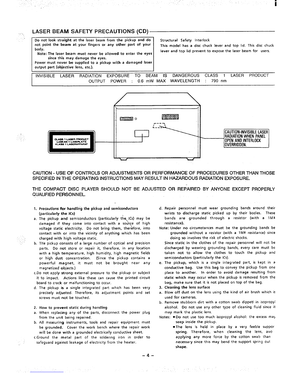
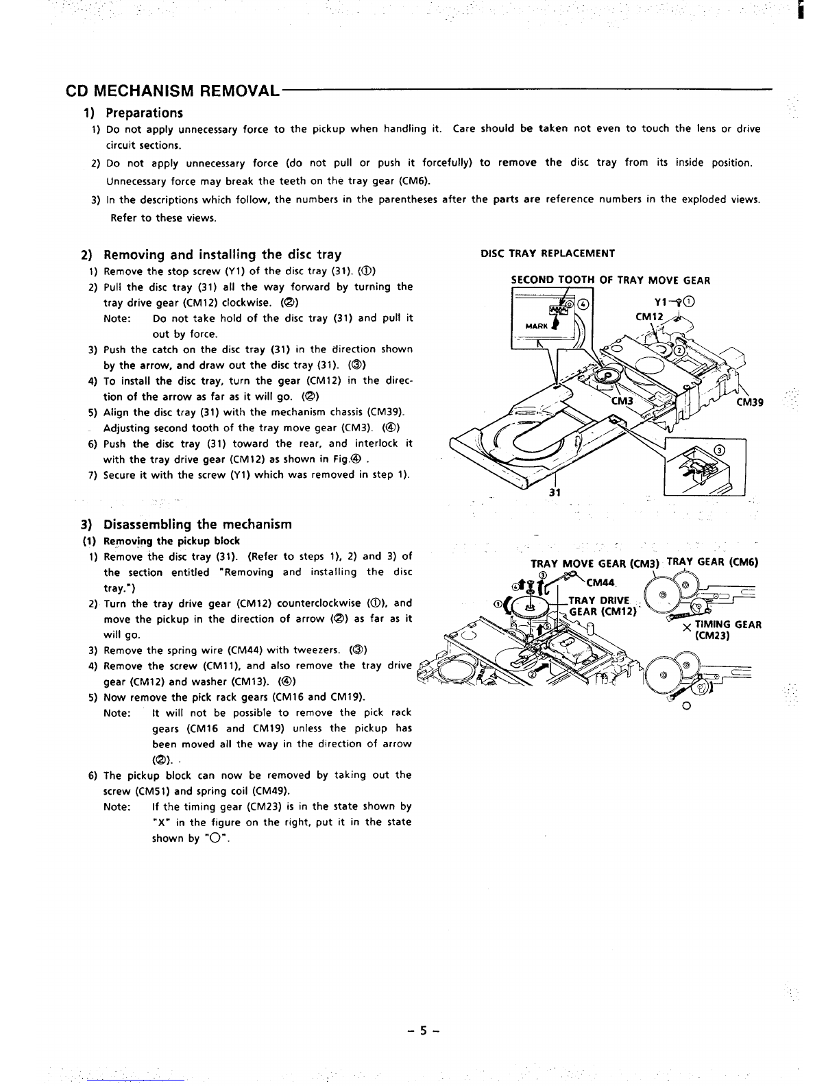
.... LASER BEAM SAFETY PRECAUTIONS (CD)
Do not look straight at the laser beam from the pickup and do Structural Safety Interlock
not point the beam at your fingers or any other part of your
body. This model has adisc chuck lever and top lid. This disc chuck
Note: The laser beam must never be allowed to enter the eyes lever and top lid prevent to expose the laser beam for users.
since this may damage the eyes.
Power must never be supplied to apickup with adamaged laser
output part (objective lens, etc.).
INVISIBLE LASER RADIATION EXPOSURE TO BEAM IS DANGEROUS CLASS 1LASER PRODUCT
OUTPUT POWER :0.6 mW MAX WAVELENGTH :790 nm
L
\/
CAUTION -USE OF CONTROLS OR ADJUSTMENTS OR PERFORMANCE OF PROCEDURES OTHER THAN THOSE
SPECIFIED IN THE OPERATING INSTRUCTIONS MAY RESULT IN HAZARDOUS RADIATION EXPOSURE.
THE COMPACT DISC PIAYER SHOULD NOT BE ADJUSTED OR REP-AIRED BY ANYONE EXCEPT PROPERLY
QUALIFIED PERSONNEL.
1.
a.
., b.
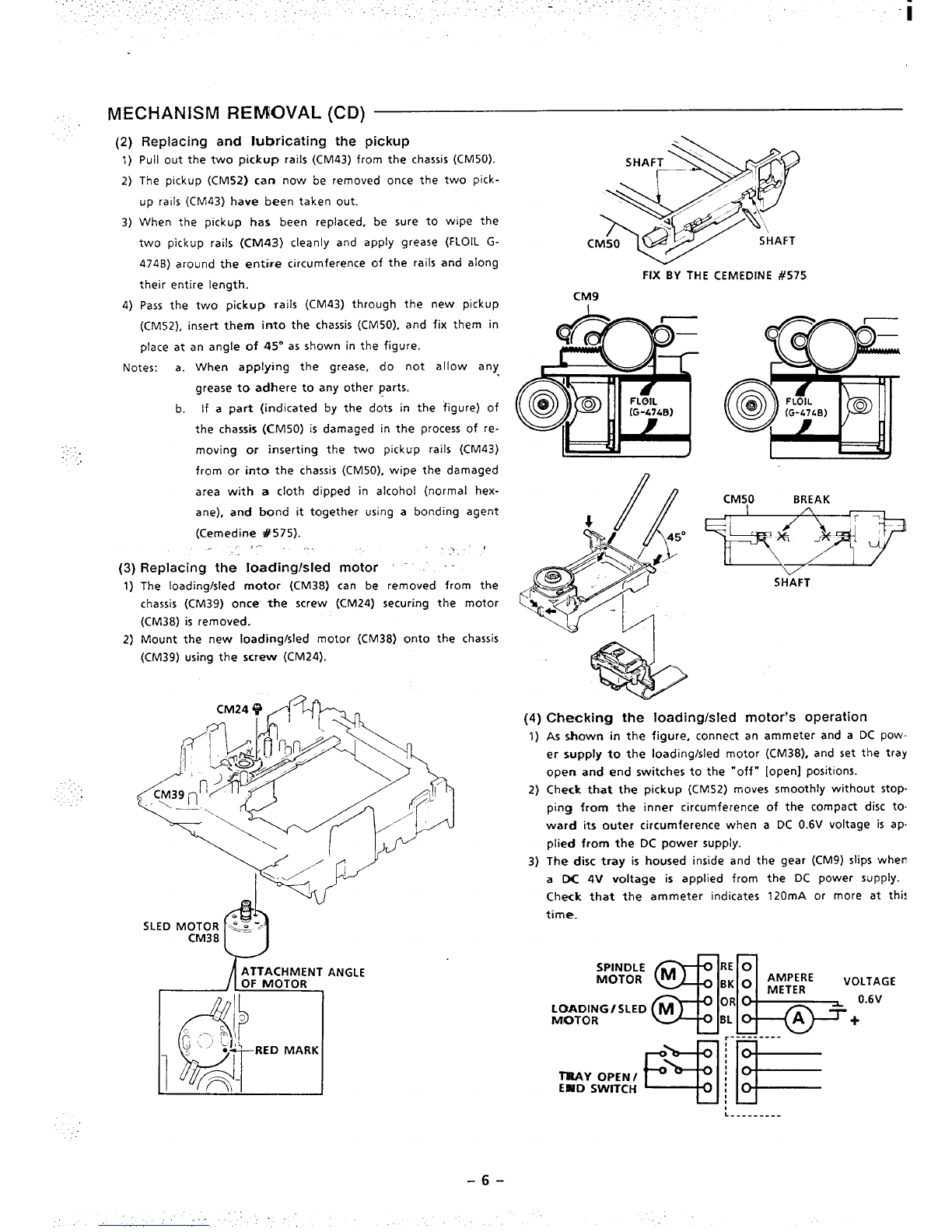
Precautions for handling the pickup and semiconductors
(particularly the lCs)
The pickup and semiconductors (particularly th lCS) may be
\
damaged if they come into contact with asou ~e of high
voltage static electricity. Do not bring them, therefore, into
contact with or into the vicinity of anything which has been
charged with high voltage static.
The pickup consists of alarge number of optical and precision
parts. Do not store or repair it, therefore, in any location
with ahigh temperature, high humidity, high magnetic fields
or high dust concentration. (Since the pickup contains a
powerful magnet, it must not be brought near any
magnetized objects.)
C.DO not apply Srong external pressure to the pickup or subject
it to impact. Actions like these can cause the printed circuit
board to crack or malfunctioning to occur.
d. The pickup is asingle integrated part which has been very
precisely adjusted. Therefore, its adjustment points and set
screws must not be touched.
2. How to prevent static during handling
a. When replacing any of the parts, disconnect the power plug
from the unit being repaired.
b. All measuring instruments, tools and repair equipment must
be grounded. Cover the work bench where the repair work
will be done with agrounded electrically conductive sheet.
c.Ground the metal part of the soldering iron in order to
safeguard against leakage of electricity from the heater.
d. Repair personnel must wear grounding bands around their
wrists to discharge static picked up by their bodies. These
bands are grounded through aresistor (with alM:
resistance).
Note: Under no circumstances must be the grounding bands be
e.
3.
a.
b.
grounded without aresistor (with a1Ml resistance) since
doing so involves the risk of electric shocks.
Since static in the clothes of the repair personnel will not be
discharged by wearing grounding bands, every care must be
taken not to allow the clothes to touch the pickup and
semiconductors (particularly the ICS).
The pickup, which is asingle integrated part, is kept in a
conductive bag. Use this bag to convey the pickup from one
place to another. [n order to avoid damage resulting from
static which may occur when the pickup is removed from the
bag, make sure that it is not placed on top of the bag.
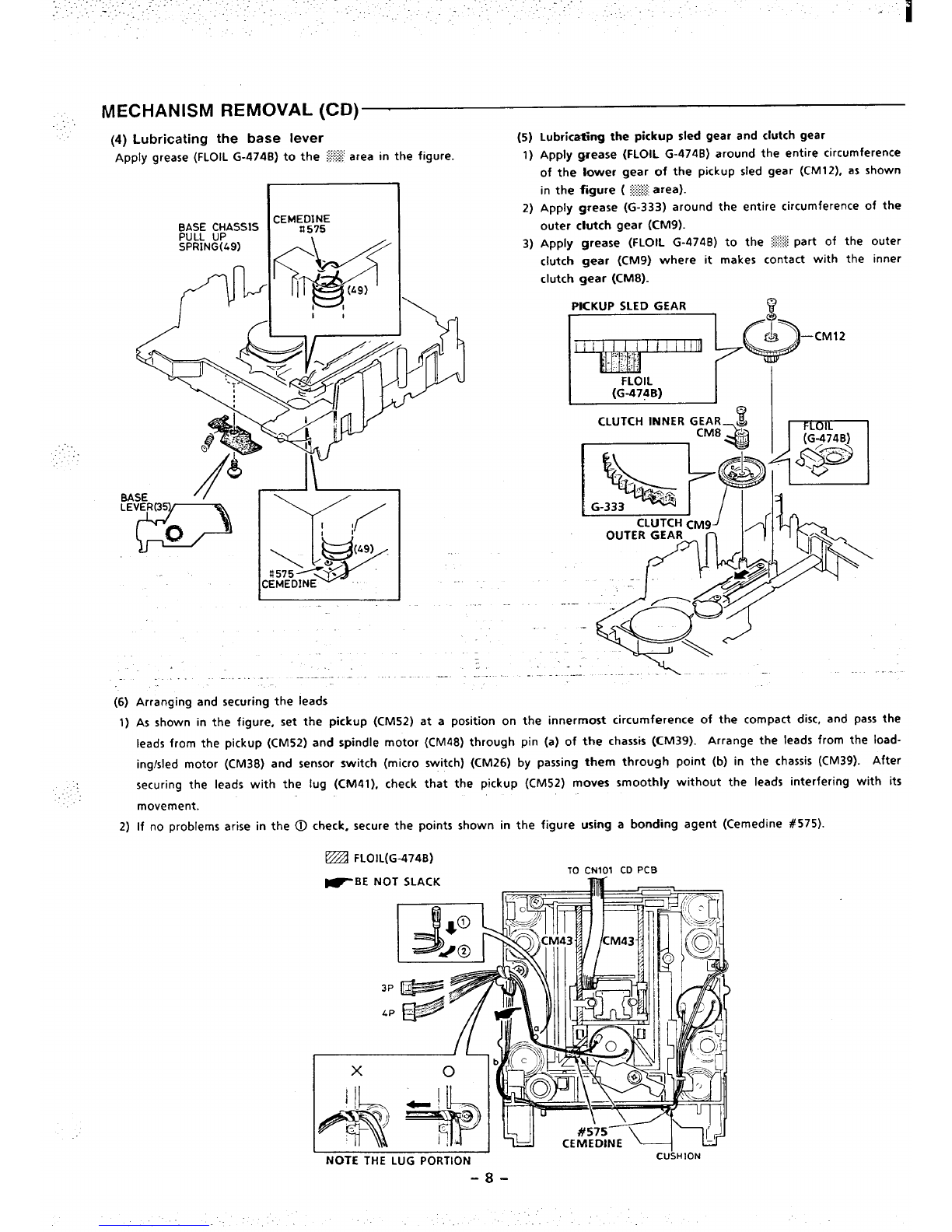
Cleaning the lens surface
Blow off dust on the lens using the kind of air brush which is
used for cameras.
Remove stubborn dirt with acotton swab dipped in isopropyl
alcohol. Do not use any other type of cleaning fluid since it
may mark the plastic lens.
Notes: ●Do not use too much isopropyl alcohol: the excess ma)
seep inside the pickup.
●The lens is held in place by avery feeble supper
spring. Therefore, when cleaning the lens, avo
applying any more force by the cotton swab than
necessary since this may bend the support spring out
shape.
-4-

‘.
CD MECHANISM REMOVAL
1) Preparations
1)Do not apply unnecessary force to the pickup when handling it. Care should be taken not even to touch the lens or drive
circuit sections.
2) Do not apply unnecessary force (do not Pull or push it forcefully) to remove the disc tray from its inside position.
Unnecessary force may break the teeth onthetray gear (CM6).
3) In the descriptions which follow, the numbers in the parentheses after the parts are reference numbers in the exploded views.
Refer to these views.
2)1)
2)
3)
4)
5)
6)
7)
3)
(1)
1)
2)
3)
4)
5)
6)
Removing and installing the disc tray DISC
Remove the stop screw (Yl) of the disctray (31). (~)
Pull the disc tray (31) all the way forward by turning the
tray drive gear (CM12) clockwise. (@)
Note: Do not take hold of the disc tray (31) and pull it
out by force.
Pushthe catch on the disc tray (31) in the direction shown
bythearrow, anddraw outthe disc tray (31). (@)
To install the disc tray, turn the gear (CM12) in the direc-
tionof thearrowas far as it will go. (@)
Align thedisc tray (31) with the mechanism chassis (CM39).
Adjusting second tooth of thetray move gear (CM3). (@)
Push the disc tray (31) toward the rear, and interlock it
with the tray drive gear (CM12) as shown in Fig.@ .
Secure itwiththe screw (Yl)which was removed in step 1).
TRAY REPLACEMENT
SECOND TOOTH OF TRAY MOVE GEAR
-,
Disassembling the mechanism
Removing the pickup block
Remove the disc tray (31). (Refer to steps 1), 2) and 3) of
the section entitled “Removing and installing the disc TRAY MOVE GEAR (CM3) TRAy GEAR (CM6)
tray.-)
Turn the tray drive gear (CM 12) counterclockwise (@), and
*R
r.
move the pickup in the direction of arrow (@) as far as it
.
will go. (CM23)
Remove the spring wire (CM44) with tweezers. (@)
Remove the screw (CM1 1), and also remove the tray drive
%’
G———————
gear (CM12) and washer (CM13). (@) @
Now remove the pick rack gears (CM16 and CM19). ‘&_’_’- .::
Note: It will not be possible to remove the pick rack u
gears (CM16 and CM19) unless the pickup has
been moved all the way in the direction of arrow
(@).
The pickup block can now be removed by taking out the
screw (CM51) and spring coil (CM49).
Note: If the timing gear (CM23) is in the state shown by
“X” in the figure on the right, put it in the state
shown by “O”.
-5-

“
MECHANISM REIWIVAL (CD)
(2)
1)
2)
3)
....
‘..
...
4)
Replacing and lubricating the pickup
Pull out the two pickup rails (CM43) from the chassis (CM50).
The pickup (CM52) cam now be removed once the two pick-
up rails (CM43) have been taken out.
When the pickup has been replaced, be sure to wipe the
two pickup rails (CM43) cleanly and apply grease (FLOIL G-
474B) around the entire circumference of the rails and along
their entire length.
pass the two pickup rails (CM43) through the
(CM52), insert them into the chassis (CM50), and
place at an angle of 45” as shown in the figure.
Notes: a. When applying the grease, do not
grease to adhere to any other parts.
new pickup
fix them in
allow any
b. If apart (indicated by the dots in the figure) of
the chassis(CM50) is damaged in the process of re-
moving or inserting the two pickup rails (CM43)
from or into the chassis (CM50), wipe the damaged
,M$q
.
SHAFT “
r.’/7’
h..
,
/’ /,
+s .- “
a
N
,. SHAFT
FIX BY THE CEMEDINE #575
CM9
area with acloth dipped in alcohol (normal hex-
ane), and bond it together using abonding agent
(Cemedine #575).
, ..
. . ..’,
(3) Replacing the” loading/sled motor ““--’
1) The loading/sled motor (CM38) can be removed from the
chassis (CM39) once the screw (CM24) securing the motor
(CM38) is removed.
2) Mount the new Ioadinglsled motor (CM38) onto the chassis
(CM39) using the screw (CM24).
(4)
1)
2)
3)
l’”QATTACHMENT ANGLE
OF MOTOR
}
o
c
~,—. m
,, ‘“k‘4 RED MARK
2
I‘#T
m-
%
00 00=
0
0
@FLOIL
(G-4746) 0
CM50 BREAK
-SHAFT
Checking the loading/sled motor’s operation
As shown in the figure, connect an ammeter and aDC pow-
er supply to the loading/sled motor (CM38), and set the tray
open and end switches to the “off” [open] positions.
Check that the pickup (CM52) moves smoothly without stop
ping from the inner circumference of the compact disc to.
ward its outer circumference when aDC 0.6V voltage is ap.
plied from the DC power supply.
The disc tray is housed inside and the gear (CM9) slips when
aDC 4V voltage is applied from the DC power supply.
Check that the ammeter indicates 120mA or more at this
time.
——
U,u L-------.-

MECHANISM REMOVAL (CD)
4)
(1)
1)
2)
Check points for CD mechanism assembly and (3)
lubrication 1)
Lubricating and mounting the tray slide
Apply grease (FLOIL G-474B) to the area indicated by the di-
agonal in the figure. 2)
When inserting the tray slide (CM15), set the position where
it is installed vis-a-vis the base/tray timing gear (CM20) as 3)
shown in the figure. 9
(2)
1)
2)
3)
>——.. .. .
%y:,:-? FLOIL(G-474B) ~<
Installing the tray gear
Move the tray slide (CM 15) in the direction of the arrow o.
Engage the gear section of the tray slide (CM15) with the
inner gear of the tray gear (cM6) at the center line, as
shown in the figure.
Align the tray move gear (CM3) with the position (0) of the
hole in the outer gear of the tray gear (CM6) and engage
the tray move gear (CM3), as shown in the figure.
TRAY
GEAR
4)
Installing the base up/down slide and timing gear
Move the base up/down slide (CM14) in the direction of the
arrow 0, and set the gears at the positions shown in the
figure.
Insert the timing gear (CM23), and mount it using the screw
(CM21).
Turn the timing gear (CM23) counterclockwise.
TIMING GEAR BASE UP/ DOWN
p@gg:$4
vSCREW (CM21)
Hook the gear tension spring (CM22) onto the timing
gear (CM23). .
@GEARTENSION ,PRING
ox
—
‘~ sGEAR TENSION SPRING (CM22)
ox
.- --
I-- --
II GEAR CM3
,..

, ., MECHANISM REMOVAL (CD)
(4) Lubricating the base lever
Apply grease (FLOILG-474B)to the >~area in the figure.
.....
(6)
1)
2)
II
..--
Arranging and securing the leads
—.
(5)
1)
2)
3)
Lubricating the pickup sled gear and clutch gear
ApplY grease (FLOIL G-474B) around the entire circumference
of the lower gear of the pickup sled gear (CM12), as shown
in the figure (%area).
Apply grease (G-333) around the entire circumference of the
outer ctutch gear (CM9).
Apply grease (FLOIL G-474B) to the *Part of the outer
clutch gear (CM9) where it makes contact with the inner
clutch gear (cM8).
PKKUP SLED GEAR
F~+-cM12
...—
OUTER GEAR “-”h ]’
.\.. ..
As shown in the figure, set the pickup (CM52) at aposition on the innermost circumference of the compact disc, and pass the
leads from the pickup (CM52) and spindle motor (CM48) through pin (a) of the chassis (CM39). Arrange the leads from the load-
ing/sled motor (CM38) and sensor switch (micro switch) (CM26) by passing them through point (b) in the chassis (CM39). After
securing the leads with the lug (CM41), check that the pickup (CM52) moves smoothly without the leads interfering with its
movement.
if no problems arise in the @check, secure the points shown in the figure using abonding agent (Cemedine #575).
TO CN101 CD PCB
~BE NOT SLACK m.
NOTE THE LUG PORTION -8-
CU\HION

SERVICE MODE ...
Specifications
To enter any service mode other than timer debugging, first simultaneously press the OPEN/CLOSE and BAND keys on the CT unit.
This accesses the service mode entry state. Now press one of the buttons on the CT unit to enter aservice mode. As the service
mode entry state is discontinued after 1second elapses, the system will enter aservice mode only if the next key is pressed within
one second.
1. Confirm the clock
.When the CLOCK key is pressed during the service mode entry state, arectangular wave with afrequency of one- fourth that
of the oscillating frequency (1 .048576MHz) is output from the micro processor’s port CLKOUT.
.The clock output is stopped by pressing either the POWER or SET CLEAR key.
2. Timer debugging
When the FAST key is pressed, the current time advances one minute and the seconds readout changes to 55 seconds. If the
key is held down the time advances continuously.
.The FAST key, aconcealed key not actually mounted to the set.
+,,,
12k ohm
Note :For timer debugging, the service mode entry state (entered by simultaneously pressin”g the 34
OPEN/CLOSE service mode entry key and the BAND key) is not necessary. FAST KEY F
3. Checking the key input signal connections
.Enter this mode by pressing the ME MORY(TUNER) key during the service mode entry state. L—
.The entire LCD goes out once this mode is entered.
.In this mode, as keys on the CT unit (or remote control unit) are pressed segments on the LCD corresponding to each key on
aone-to-one basis come on (i.e. the lit portions gradually increase). (Refer to Table 1.)
KEY DISPLAY KEY DISPLAY KEY DISPLAY
TIME /FADE TIME CLOCK REC FUNCTION DIGIT 3: H
REPEAT REPEAT SLEEP SLEEP BAND DIGIT 4: H
STOP ONE TUNING UP SIDE APST UP 1OF CALENDAR
CD MEMORY PROG. TUNING DOWN SIDE BPST DOWN 2OF CALENDAR
PLAY IPAUSE >WAKE UP WAKE UP FMITUNE MODE 3OF CALENDAR
RANDOM RANDOM TIMER TIMER WIDE 4OF CALENDAR
OPEN /CLOSE ALL SET ICLEAR @FW DDISC
EDIT EDIT MEMORY 5OF CALENDAR BACK TRACK
COMPUTER REC COMP. REC POWER DIGIT 2:~.:...
@:Releases the key checking mode and returns the set to the normal mode.
TABLE 1:CORRESPONDING KEYS AND DISPLAYS IN THE KEY CHECKING MODE
COMPUTERREC, WIDE CLOCK INTRO RANDOM OFF SIDEA
;;::u;–/–/f/Tllb/-//–/;!-2 51/-//-/’/–//:/ ;;;;;B
LEVEL /~/d”/c/~//~/ LWAM-( /~//~/~/&/~/MHz PM
TIMERREC DiscST TRACK AUTO MONO FADETIMEEDIT
REPEAT
P
m123456789101112131415 ~ONEALLCONT
FIGURE 1:LCD( LIQUID CRYSTAL
-9-
DISPLAY )

,.
SERVICE MODE
. .
4. Checking LCD connections
-Enter this mode by pressing the OPEN/CLOSE key during the service mode entry state. (See note.)
.The entire LCD goes out once this mode is entered.
In this mode, one segment of the LCD lights each time the OPEN/CLOSE key is pressed.
.Press the SET/CLEAR key to exit this mode and return to the normal mode.
5. System connector checking mode
Enter this mode by pressing the BAND key during the service mode entry state.
Before entering this mode, connect ajig at the beginning of the system connector cord as shown in Figure 2
In this mode, check the signal connections shown in Table 2for the set’s CT unit and system connector cord.
The results of the checking of connections appear on the LCD as shown in Table 2.
Press the SET/CLEAR key to release the system connector checking mode and return to the normal mode.
rCT UNIT SYSTEM CON-
NECTOR CORD JIG
.,
FIGURE 2“:-CONNECTION ‘DURING THE SYSTEM
CONNECTOR--CHECKING MODE --
2.2k
~
GND
BUSY
TA-AF
DUB-IN
so
SCK
IR
KEY-O
FIGURE 3-: CIRCUIT DIAGRAM OF THE
CONNECTOR CHECKING JIG
.- STATE DISPLAY STATE DISPLAY
Sois N.G. .“ ,,- -- “o” BUSY is N.G. 4
SCK is N.G. 1IR is N.G. 5
DUB-IN is N.G. 2KEY-O is N.G. 6
AT-AF is N.G. 3All OK
Note: :With the Dseries, the system connector checking mode cannot be entered when the SCK(AD unit) connection is defective.
TABLE 2: DISPLAYS DURING SYSTEM CONNECTOR CHECKING
6. CD tracking balance adjusting mode
.Enter this mode by pressing the PLAY/PAUSE key during the service mode entry state.
.If the power is off when this mode is entered, the power automatically comes on.
.In this mode, the tracking balance adjustment state (tracking is off) is automatically entered after the tray is completely closed.
If the PLAY key is pressed in this state, the ~racking servo is turned on and playing is begun at the present position.
Therefore, the readout on the display at the time playing is begun indicates the initial position of the pickup (i.e. the position
of the limit switch).
.In this mode, the tracking balance adjustment state can be entered by pressing
PLAY key in this state turns on the tracking servo and causes playing to begin.
.Turning off the power releases the CD tracking balance adjusting mode.
7. CD operatiort display mode
.Enter this mode by pressingthe STOPkey during the service mode entry state.
the MEMORY key during playing. Pressing the
.If the power is off when this mode is entered, the power automatically comes on.
-1o-

SERVICE MODE
.In this mode, when CD function are used, displays like those shown in Table 3(which represent CD operations different than
normally displayed) appear in the LCD track number display.
.In this mode, the calendar numbers shown in Table 4come on when an error occurs in CD operations, at which time the
track number and calendar displays become fixed at their current readouts. To release these fixed displays, press the STOP key
while operations are stopped.
.This mode is released when the power is turned off.
IDISPLAY IOPERATION I
nu FOCUSsearch has been begun
U1 Focus search has been begun
❑zWaiting for focusing
Is-l I
Spindle kick is in progress
:2 ]Both CLV and tracking are ON
fi~ Both CLV and tracking are ON
n- Focus search has been completed (success, failure)
20 Tray closing has begun
21 Tray closing is in progress
Zz Pick return (internal direction) is in progress
~~ Pick return (external direction) is in progress
z- Tray closing (pick return) has been completed
an Spindle braking has bequn
Ell Spindle braking is in progress
g~ Pick return is in progress
I3- ]Spindle braking and pick return have been ..
completed
~il Fast forwarding is in progress
ql Rewinding is in progress
~n Plavina has beoun
51 Playing is in progress
~~ Playing is in progress (skip return operation)
En TOC reading has been begun
I~I I TOC readin~ is in proqress I
INUMBER
E
4
5
6
7
IDISPLAY IOPERATION I
6Z TOC reading is in progress
6- TOC reading has been completed (success/failure)
10 L-point access has been begun
II L-point access (REV64 track jump)
12 L-point access (FWD64 track jump)
13 L-point access (REV16 track jump)
qq L-point access (FWD16 track jump)
Is L-point access (REV1 track jump)
16 L-point access has been completed
Hn Pausing has begun
E3 Pause (REV16 track jump)
H~ Pause (FWD16 track jump)
❑sPause (REV1 track jump)
HE Pause (trace)
9U Music acc”esshas begun
91” Music access (high-speed access has begun)
g~ Music access (high-speed access is in progress)
93 Music access (high-speed access has been completed)
9q Music access (high-speed access has been completed)
95 Music access (high-speed access has been completed)
96 Music access (REV64 track jump)
91 Music access (FWD64 track jump)
99 Music access (REV16 track jump)
99 Music access (FWD16 track jump)
9- Music access (final stage)
TABLE 3:DISPLAYS DURING THE CD OPERATION MODE
STATE OF CD ERROR
Focusing is not possible in focus search.
The subcode is not input during disc startup.
TOC cannot be read.
The focus was lost while the servo was on (during playing, etc.).
The subcode is not input while the servo is on (during playing, etc.).
The tray does not open completely.
The tray does not close completely.
TABLE 4:DISPLAY OF CD ERRORS
-11-
.. .

CD ADJUSTMENT
Electrical Adjustment 10K
So far we have presented explanations regarding compact disc
player handling, notes prior to repair, handling the pick-up and
disassembly of the unit. Be sure to carefully read these ‘r;::D–A*’’O-’cO”
instructions before making any adjustments. BAND PASS FILTER
Preparations for Adjustments
Measuring instruments, tools and filter (4) Oscillator (400 Hz, 300mV RMS)
(1) Test disc. :YEDS lB (Sony) (5) Frequency Counter (5MHz; or more)
(2) Oscilloscope: SS5711 (IOMHZ or dual phenomenon) (6) Screw drivers (non-metalic) for adjustments
or Memoryscope :DSS6521 (Storagescope) (7) Band Pass Filter
(3) Digital voltmeter (Input impedance 1Mohm or more) (B) AC Voltage Meter
Notes :a. The adjustments can be using the equipment produced by other manufactures provided that the performance of that
equipment corresponds to that of the above listed models.
b. Use a10:1 probe for observing signals on the oscilloscope and stora9e scoPe.
c. Test disc is subject change without notice.
1. Initial set
., Set the SVR11 at its initial position of adjustment controls as shown in figure below.
SVR11
INITIAL SET
(MECHANICAL
SENTER)
..
2. Tracking Balance Adjustment (SVRII)
1.
2.
3.
4.
Connect the oscilloscope to TP3 (TE) and TP4 (GND.).
Turn on the power of the unit. Insert test disc.
Play-back the test disc.
Continuously press the forward search } } or backward-
search } } button to do it
TP 1
(RF)
TP3
(TE) Ov
-SEARCH
-12-
SVRI 1
TP2 (FE)
TP3 (TE)
TP4 (GND)
TPI (RF)
5. Adjust SVR11 so that the TE (Tracking Error) signal wave
form of TP3 on the oscilloscope is vertically symmetrical rel
ative to OV. (See figure right side)
“If the adjustment is imperfect, become run away the sled
motor (pick-up sending motor), inferior playability.
Ov
SEARCH h

..- ..---- .. . . i
.---- . .
‘-*. ., ;. ...
,.? ,.. ,
CD ADJUSTMENT
2. Other Adjustment of Tracking Balance (SVR11) ~-=~-l’ “
1.
2.
3.
4.
Set the service mode(CD tracking balance adjusting mode).
Enter this mode by pressing the PLAY/PAUSE key during TP1
the service mode entry state. Pressing the PLAY /Pause key (RF)
in this state turns on the tracking servo and causes playing
to begin. (See service mode)
Connect the oscilloscope to TP3 (TE) and TP4 (GND).
Adjust SVR1 1so that the TE (Traverse) signal waveform of TP3 Ov
TP3 on the oscilloscope is vertically symmetrical relative to (TE)
OV. Or may adjust SVR11 so that the DC voltage :(Peak
Hold Level) -(Bottom Hold Level) of the traverse signal is
OV. (See figure right side)
If it were not for obtain waveform at the right figure, re-
peat item 2-1 -2-3.
3. Focus Gain Confirmation
1. Connect the storage scope to TP2 (F.E :Focus Error) 4. Set the output of AF oscillator to 400 Hz, 0.5V rms and
through the Band pass filter. (See BPF Figure) connect to pin 24 (IC101) through the resistor :120k ohms.
2. Turn on the power of the unit. 5. Confirm so that the voltage of the F.E signal waveform
3. Play-back the test disc. on the storage scope is 0.5V p-p, f3db by through BPF.
‘If this
Disc. CONFIRMATION is imperfect, become weak the mechanical shock, inferior playability, and can not playback the
. .
AF OSCILLATOR MAIN PCB OSCILLOSCOPE or STORAGESCOPE
400Hz 120K BAND PASS FILTER
~Iclol
1. Je-.
.-
0.5; rms -DIM 74 TP2
(FE)
==
I,,,.,-
1I
4. Tracking Gain Confirmation
1. Connect the storage scope to TP3 (T.E) through the Band 4. Set the output of AF oscillator to 400Hz, 0.5V rms and
pass filter. (See BPF Figure). connect to pin 14( IC101) through resistor 47k ohms.
2. Turn on the power of the unit. 5. Confirm so that the voltage of T.E signal waveform
3. playback the test disc. storage scope is 0.5V p-p, f3db by through BPF.
‘If this CONFIRMATION is imperfect, become weak the mechanical shock, inferior playability, and can not playback the Disc.
AF OSCILLATOR MAIN PCB OSCILLOSCOPE or STORAGESCOPE
400Hz 47K BAND PASS FILTER
Iclol
0.5V rms PIN 14 TP3
(TE) Iu ~_E–.
==
on the

-----.-,
.,..
PARTS LIST
PRODUCT SAFETY NOTICE
Each precaution in this manual should be followed during servicing. Components identified with the IEC symbol Ain the parts list
and the schematic diagram designate components in which safety can be of special significance. When replacing acomponent identi-
fied ~, use only the replacement parts Clesignateci, or parts with the same ratings of resistance, wattage or voltage that are desig-
nated in the parts’ list in this manual. Leakage-current or resistance measurements must be made to determine that exposed parts
are acceptably insulated from the supply circuit before returning the product to the customer.
CAUTION: Regular type resistors and capacitors are not list. To know those values, refer to the schematic diagram.
N.S.P :Not avairable as service parts.
:ABINET
Ref. No.
1
2
3
4
5
6
7
8
9
10
11
Part No.
614 238 9966
614 239 0924
614 244 4009
614 239 0931
614 239 1082
614 239 1136
614 239 1143
614 239 1150
614 239 1167
614 239 1174
614 239 1181
:HASSIS :
Ref. No.
31
32
33
34
35
36
37
38
FIXING PARTS
Part No.
614 238 1694
614 239 1228
614 239 1198
614 239 1204
614 239 1211
614 195 6978
412 003 1708
614 212 8343
r-.~<: ’s-
Ref. No. Part No.
Y1 411 022 8408
T2 411 021 1202
Y3 411 021 3107
Y4 411 021 1806
Y5 411 021 6405
Y6 411 021 6603
Y7 411 021 3503
ELECTRIC PARTS
Description
ASSY,PANEL,FRONT
ASSY,CA81NET,TOP
PANEL,REAR
ASSY,CA81NET,BOTTOM
ESCUTCHEON,CDTRAY FRONT
BUTTON,TIMER ETC.
BUTTON,BAND ETC.
BUTTON,TUN,PRESET
BUTTON,CD
BUTTON,CDSKIP
BUTTON,CDOPEN/CLOSE
Description
TABLE,LOADING,CD
MOUNT-M,CD MECHA
BRACKET-E,TU PCB
BRACKET-E,CD PCB
hfOUNT-E,TU PCB
RUBBER CUSHION,MECHA FLOAT
SPECIAL SCREW,MECHA FIX
LABEL,LASER BEAM CAUTION
Description
SCR S-TPG PAN 2X8
SCR S-TPG BIN 2X8
SCR S-TPG BIN 2.6X8
SCR S-TPG BIN 2.6X1O
SCR S-TPG BIN 3X8
SCR S-TPG BIN 3X8
SCR S-TPG 81N 3X1O
Ref. No. Part No. Description
51 614 243 1481 CORD,CDMECHA-MICON PCB
WNER P
Ref. No.
71
C2304
C2458
CF201
CF202
CF204
CF205
:.BOARDASSY
Part No.
614,247 6561
6S4 116 5349
614 117 1029
4Q3 080 5000
4~3 106 1603
614 231 0199
6S.4 231 0199
614 208 9644
614 030 4787
Description
ASSY,PCB,TUNER MAIN
SHIELD PLATE,SYMBOL SIDE
SHIELD PLATE,PATTERN SIDE
POLYPRO 1000P J100V
NP-ELECT lU Q50V
FILTER,1O.5MHZ,FM
FILTER,1O.5MHZ,FM
FILTER,450KHZ,AM
CERAMIC FILTER,450KHZ
-14-
Ref. No.
CN201
CN241
CT201
D2101
D2102
D2103
D2104
or
or
D2105
or
or
D2201
or
or
D2301
or
or
D2302
or
or
IC201
IC202
IC203
L2102
L2103
L2104
L2105
L2150
L2451
Q2101
or
Q2102
Q2103
or
Q2104
Q2105
Q2201
Q2202
or
Q2203
Q2301
or
Q2302
or
or
Q2351
or
or
Q2352
or
or
Q2451
or
Q2452
cm
Part No.
614 239 1686
614 225 3502
614 007 6356
407 105 0100
407 105 0100
407 io5 0100
407 007 9904
407 012 4406
407 012 5809
407 007 9904
401 012 4406
407 012 5809
407 007 9904
407 012 4406
407 012 5809
407 007 9904
407 012 4406
407 012 5809
407 007 9904
407 012 4406
407 012 5809
409 195 3108
409 016 9500
409,066 7600
614 229 0866
614 229 0873
614 239 7282
614 028 4058
614 241 1162
614 028 4256
405 114 8407
405 114 8506
405 012 5904
405 114 8407
405 114 8506
405 012 5904
405 012 5904
405 018 7902
405 012 2002
405 020 7204
405 001 7001
405 012 2002
405 020 7204
405 067 0800
405 078 2404
405 000 0904
405 067 0600
405 078 2404
405 000 0904
405 067 0800
405 078 2404
405 000 0904
405 114 1804
405 114 1903
405 114 1804
405 114 1903
Description
TERMINAL,4P,ANT
PLUG,14P,T0 FRONT
TRIMMER,llPF,WH
VARAcTOR01 SVC211-B-AL
VARACTOR 01 SVC211-B-AL
VARACTOR DI SVC211-B-AL
DIODE GMAO1
DIODE 1SS133
DIOOE 1SS176
DIODE GMAO1
DIODE 1SS133
DIODE 1SS176
DIODE GMAO1
DIODE 1SS133
DIODE 1SS176
DIODE GMAO1
DIODE 1SS133
DIODE 1SS176
DIODE GMAO1
DIODE 1SS133
DIODE 1SS176
IC LA1265-AUD
IC LA3361
IC LM7001
TRANS,RF,FM
TRANS,RF,FM
TRANS,OSC,FM
FILTER,CHOKE,2.2UH,FM
TUNER,RF,AM
FILTER,CHOKE, 1OOUH,VDD
TR 2SK193-LL
TR 2SK193-ML
TR 2SC1923-Y
TR 2SK193-LL
TR 2SK193-ML
TR 2SC1923-Y
TR 2SC1923-Y
TR 2SC380TM-O
TR 2SC1815-GR
TR 2SC945A-K
TR 2SA1015-GR
TR 2SC1815-GR
TR 2SC945A-K
TR RN2207
TR BN1A4P
TR DTA114YS
TR RN2207
TR BN1A4P
TR DTA114YS
TR RN2207
TR BN1A4P
TR DTA114YS
TR 2SC1815(L)-GR
TR 2SC1815(L)-Y
TR 2SC1815(L)-GR
TR 2SC1815(L)-Y

PARTS LIST
Ref. No. Part No. Description
Q2461 405 012 2002 TR 2SC1815-GR
or 405 020 7204 TR 2SC945A-K
Q2701 405 012 2002 TR 2SC1815-GR
or 405 020 7204 TR 2SC945A-K
Q2702 405 016 2206 TR 2SC2878-A
or 405 016 2305 TR 2SC2878-B
Q2801 405 012 2002 TR 2SC1815-GR I
or 405 020 7204 TR 2SC945A-K
Q2802 405 016 2206 TR 2SC2878-A
or 405 016 2305 TR 2SC2878-B
R2465 &401 018 1209 CARBON 33 JB l/4W
SVR23 614 223 1906 POTENTIOMETER, 1OK(B),VCO
or 614 204 1901 SEMI-FIXED V.R,1OK(B),VCO
T2201 614 239 7299 TRANS,IF,FM
T2202 614 030 4114 I.F.T,1O.7MHZ,FM
X2451 614 240 1118 RESONATOR,7.2MHZ
or 614 234 0486 RESONATOR,7.2MHZ
:D MICON P.C.BOARD ASSY
Ref. No. Part No. Description
72 614. 239 2065 ASSY,PCB, CO MICON
C1301 403 196 9602 DL-ELECT 0.047F Z5.5V,FOR
MICON BACKUP
C1302 4Q3 135 3302 ELECT 1000U M6.3V
C1522 403 056 7908 POLYESTER 1000P K50V
C1523 403 056 790B POLYESTER 1000P K50V
C1608 403 043 3104 ELECT 2200U M16V, FOR +9V
C1609 403i 042 6205 ELECT 1000U M16V, FOR -9V
CN131 614 225 6459 PLUG,13P,CO-FRONT
CN132 614 225 6381 PLUG,6P,CD-FRONT
CN141 614 241 6143 SOCKET,22P,CD-MECHA
614 243 3218 SOCKET,22P,CD-MECHA
%161 614 2395455 SOCKET,19P,CT-DA UNIT .
D1301 407 005 4505 DIODE DS442X
or 40F 013 7109 DIODE 1S2473
D1302 407 050 1801 ZENER OIODE GZA3.9Z
or 407’ 053 5202 ZENER DIODE MTZ3.9B
01303 40T 005 4505 DIODE DS442X
or 407 013 7109 DIOOE 1S2473
D1304 407 005 4505 DIODE DS442X, FOR IR
or 407 013 7109 DIODE 1S2473,FOR IR
D1601 A407004 9105 D1ODE DSF1OC
or A407 012 3300 OIODE 1SR35-200A
01602 A40TO04 9105 DIOOE DSF1OC
or A40~ 012 3300 DIODE 1SR35-200A
D1603 A407’ 004 9105 DIOOE DSF1OC
or A407 012 3300 DIODE 1SR35-200A
D1604 A407 004 9105 DIODE DSF1OC
or A407’ 012 3300 DIODE 1SR35-200A
D1605 40~ 013 7109 DIODE 1S2473
or 40Z 005 4505 DIODE 0S442X
IC103 41C# 146 1104 IC UPD75116GF-F56-3BE
IC107 ~409 189 4203 IC M5278005
IC108 40% 040 1105 IC NJM79L05A
IC109 40S 039 9204 Ic NJM7BL05A
L1301 61A! 028 4133 FILTER,CHOKE,1OUH
L1501 614? 212 3171 INOUCTOR,FERITE,CD OUT L-CP
L1502 61* 212 3171 INC)UCTOR,FERITE,CD OUT R-Ch
Q1301 4E% 006 1806 TR 2SA933S-R
or 40% 006 1905 TR 2SA933S-S
405 002 1305 TR 2SAI048-Y
;i302 4@S 011 85oO TR 2SC1740S-R
or 405 011 8609 TR 2SC1740S-S
405 014 5209 TR 2SC2458-GR
;:303 405+ 006 1806 TR 2SA933S-R
Ref. No. Part No. Description
or 405 006 1905 TR 2SA933S-S
405 002 1305 TR 2SA1048-Y
;304 405 011 8500 TR 2SC1740S-R
w405 011 8609 TR 2SC1740S-S
405 014 5209 TR 2SC2458-GR
;305 405 006 1806 TR 2SA933S-R
cm 405 006 1905 TR 2SA933S-S
405 002 1305 TR 2SA1048-Y
;500 405 011 8500 TR 2SC1740S-R
er 405 011 8609 TR 2SC1740S-S
405 014 5209 TR 2SC2458-GR
;;501 405 011 85oO TR 2SC1740S-R
car 405 011 B609 TR 2SC1740S-S
or 405 014 5209 TR 2SC2458-GR
S1301 614 221 8327 SWITCH,TACT,RESET
X1301 614 229 3300 RESONATOR,XTAL, 4.19MHZ
DMAIN P.C.BOARD ASSY
Ref. No. Part No. Description
33 614 239 2072 ASSY,PCB,CO MECHA
Chllol 614 227 7935 SOCKET,13P,FOR PICIUJP(FFC)
CN102 614 017 3833 PLUG,4P,FOR MOTOR
CN103 614 017 3B26 PLUG,3P,FOR SWITCH
CN104 .614 035 2061 SOCKET,22P,T0 CD MICON(FFC)
or -614 243 3225 SOCKET,22P,T0 CO MICON(FFC)
Iclol- “-- 409 245-4802 IC LA921OM
IC102 ~ 409 247 0000 IC LA6524
IC104 409 248 8708 IC LC7866E
IC105 409.278 0109 IC SM5870DS
1C106 409 241 5506 IC XRA15218F
or 409 192 7109 IC BA15218F
Qlol 405 002 030B TR 2SA1037K-R
Q102, 405 014 4509 TR 2SC2412K-R
Q103 405 014 4509 TR 2SC2412K-R
SVRll 614’223 1906 POTENTIOMETER”, 1OK(B),T.BAL
TP101 614 227 6839 TERMINAL,TEST POINT,RF
TP102 614 227 6839 TERMINAL,TEST POINT,FE
TP103 614 227 6839 TERMINAL,TEST POINT,TE
TP104 614 227 6839 TERMINAL,TEST POINT,GND
TP105 614 227 6839 TERMINAL,TEST POINT,PLL
Xlol 614 236 1B18 RESONATOR, 16.93MHZ
‘RONTP.C.BOARD ASSY
Ref. No. Part No. Description
74 614 244 2265 ASSY,PCB,FRONT
614 241 9151 REFLECTOR,LCD
614 238 8037 SHEET,LCO
411 021 3107 SCR S-TPG BIN 2.6X8
Cti251 614 221 9133 SOCKET,13P,CD MICON PCB
CN252 614 221 9065 SOCKET,6P,CD MICON PCB
CN253 614 226 24BI SOCKET,14P,TUNER PCB
D2501 407 013 1701 DIODE 1S1588
or 407 013 7109 DIODE 1S2473
or 407 005 4505 DIODE DS442X
212502 407 013 1701 DIODE 1S15B8
or 407 013 7109 DIODE 1S2473
or 407 005 4505 DIOOE DS442X
1C251 410 146 1203 IC UPD75306GF-225-3B9
L2501 614 028 4256 FILTER,CHOKE,1OOUH
LCD21 614 238 0284 LCD(LIQUID CRYSTAL OISPLAY)
S2511 614 220 5563 SWITCH,TACT,OPEN/CLOSE
S2512 614 220 5563 SWITCH,TACT,PLAYI’PAUSE
S2513 614 220 5563 SWITCH,TACT,STOP
-%5-

I
m
II
I
.
<I
.ncn. .n.n.nmmmm mmc+mmmmmmm m.- ~
-. 0.-”--- I- I.-.-l-”-. ......- *
*A*-a a-A*-- -- ***---*-* *a
NN,-. ?.JI.JNNNNN NNWNNNNNNN N-w z
-t4cmmJlw NNru NmJNNNNNf-.N .*NN- O
U.. rue-a.o.oo 0-00.00.00 000 .
IT C-lnnnnnnnnn nnnmnnnnnmn nn
I-1-r rvl-l-r r-r- rrrl-rrl-l-rr .F 1-r
!,,,,!,!! !!l! 1!!,, f,,,,,
+.-.,-t-.-”.. . . . . . . . . -.-..-*.-.
---l+.<-. +--J-.4.-4-J -l. ..-I. .-l
00000000000 00000000000 00 g
clct~o’a~yymmo Clrn’amyclmmmmm ma *
,, ,,, !!!! ,,, !,! .
rlrln AA1-ionn. -“m”” ”A Ann nmnn q
000000000 Oooaooooo CJwooyy ~
,,l! 1,!!! !!!! 11,,, $,,
nmDou. Dnm Dmm Dna. Dn. >n.>nm> =
rI-rx8sr Fr8 xssszrr r.. 8=.8 ~
.
(
i

EXPLODED VIEW (CD MECHANISM)
I
PARTS LIST (CD MECHANISM)
:D MEC
Ref. No.
CMO1
CM02
CM03
CM04
CM05
CM06
CM07
CM08
CM09
or
CM1O
CM1l
CM12
CM13
CM14
CM15
CM16
CM17
CM18
CM19
cp20
CM21” -‘
CM22
CM23
CM24.. .
CM25
CM26
CM27
CM28
CM29
CM30
iNISM (PM-DAD
Pan No.
411 119 8908
411 087 4704
614 224 2056
411 119 6908
411 087 4704
614 224 2049
411 152 4301
614 237 9172
614 23t 4194
614 243 6455
412 031 2104
411 152 4301
614 224 1998
412 045 4101
614 233 6311
614 224 2094
614 224 2018
412 031 2104
614 225 0684
614 224 2001
614 224 2032
412 031 2104
614 242 8665
614 237 8304
411 044.7205
614 016 9223
614 016 9223
614 202 5277
411 020 9603
614 224 1967
614 243 2594
:X22S/SP)
Description
SCR S-TPG PAN 2X14, GEAR FIX
WASHER V2X6 X0.4, GEAR FIX
GEAR TRAY MOVE
SCR S-TPG PAN 2X14, GEAR FII
WASHER V2X6 X0.4, GEAR FIX
GEAR, TRAY
SCR S-TPG PAN PCS 1.7x6
ASSY, GEAR, CLUTCH INNER
GEAR, CLUTCH OUTER
GEAR, CLUTCH OUTER
SPECIAL SC REW, SLIOE FIX
SCR S-TPG PAN PCS 1.7x6
GEAR, PICK SLED
SPECIAL WASHER, PICK GEAR
SLIOE ,BASE UP/OOWN
SLIOE, TRAY
GEAR, PICK RACK UPPER
SPECIAL SC REW, GEAR FIX
SPRING, COMP, RACK BACK
GEAR, PICK RACK LOWER
GEAR, BASE/TRAY TIMING
SPECIAL SCREW, GEAR FIX
SPRING, TENS, GEAR TENSION
GEAR, TIMING
SCR PAN+SW 2X4 ,SLEO MOTOR
SWITCH, LIMIT
SWITCH, TRAY OPEN
SPRING PLATE, CHUCKING
SCR S-TPG BRZ+FLG 3x6
BRACKET-M, CHUCKING
ASSY, PULLEY
Ref. No.
CM31
CM32
CM33
CM34
CM35
CM36
CM37
CM38
CM39
or
CM40
CM41
CM42
CM43
CM44
CM49
CM50
CM51
CM52
or
CM53
CM54
%55
or
CM56
CM57
Part No. Description
411 022 7B07 ;SCR S-TPG PAN 2X6,6 RACXET
614 224 3176 BRACKET-M, TRAY GUIOE(L)
411 022 7607 SCR S-TPG PAN ZX6,6RACKET
614 224 3183 BRACKET-M, TRAY GUIDE(R)
614 233 6304 LEvER, BASE
614 226 5536 SPRING, COMP, BASE LEVER MOVE
411 020 9902 SCR S-TPG BRZ+FLG 3x8, LEvEF
614 225 4B20 ASSY, MOTOR ,LOAOINGISLEO
614 228 5855 CHASSIS, LOADING CHASSIS
614 242 6641 CHASSIS, LOAOING CHASSIS
412 031 2i04 SPECIAL SCREW, REINFORCEMENT
614 129 9136 LUG. WIRE DRESS
411 021 5705 SC R” S-TPG BIN 3x6, LuG FIX
614 230 0411 SHAFT, PICK RAIL
614 229 4529 SPRING, WI RE, PICK BACK
614 228 5064 SPRING, TENS,6ASE PULL UP
614 247 1950 ASSY, CHASSIS, BASE CHASSIS,
WITH SPINOOLE MOTOR +TURN-
TABLE, SERVICE ONLY
411 020 98o3 SCR S-TPG BRZ+FLG 3x6
614 239 1303 PICXUP, LASER, PLASTIC
,,SF-PIPS)
614 231 6047 PICKUP .LASER. ALMINUM
T
614 246 2959 ASSY, CONNECTOR-S,4P,
614 246 2966 SPINOLE/SLEO MOTOR
614 246 2973 ASSY, CONNECTOR-S,3P,
614246- 29B0 LIMIT/TRAY OPEN SWITCH
412 014 2800 SPECIAL WASHER, GEAR FIX
614 125 6526 CUSHION, MOTOR LEAO FIX
.-.
-18- –19-

ii
,.,.’-.
IC BLCMCK DIAGRAM (CD)
ICIO1 IJWI1OM (Servo Signal Processor)
~NO. PIN NAME 1/0 FUNCTION No. PIN NAME 1/0 FUNCTION
1NC Non Connection 41 NC Non Connection
2VEE -5V 42 JP- 1-Input of Track Jump Pulse Amp[lfier
3EIIV Convert Input (from Photo D;ocie E) 43 JP+ I+Input of Track Jump Pulse Arnc’ ‘ier
4FIIV Convert Input (from Photo diode F) 44 THLD IHold of Output Voltage of Tracking Serv
—
5FN 1IV Converter Input 45 TGL1. Tracking Gain Low
6FCl oIV Converter Output 46 TOFF IInput For Off the Tracking Servo
7TE&O oTracking Error Ampl!fler Output 47 TES oTracking Error Signal
8VREF2 IReference Voltage 248 HFL oDetect Track Signal
9VRE!=3 IReference Voltage 349 FZD oDetect SCarve of Focus Error Signal
10 TEST —ITest Input 50 FOCS I Input For Off the Focus Servo
11 ATSC I+Input of Anti Shock Detect Amplifier 51 CLV- 1-Input of CLV Error Amplifier
12 AT5C- 1-Input of Anti Shock Detect Amplifier ‘52 CLV +I+Input of CLV Error Amplifier
13 TPA -+ I-Input of Tracking Pulse Amplifier 53 SLCO oSlice Level Control Amplifier Output
14 TPA- 1+lnDut of Trackina Pulse Am Dlifier 54 —
EFMO iEFMO (RF) Siqnal
15 TPAO oTracking Pulse Amplifier Output 55 Al I I EFMO (RF) Signal
16 TOFS IInput for Tracking Offset 56 VDD I+5V
17 THDS ITrackina Servo Hold Switch 57 PDO I+Input of VCO Control Amplifier
18 TO++ IAdd the Track Jump Pulse 58 PDO- 1-Input of VCO Control Amplifier
19 JPO oTrack Jump Pulse Amplifier Output 59 Vcoc IVCO Control Amplifier Output
20 SLEQ IInput for Sled Servo Equalizer 60 Vcoo oVco output
21 TDO oTracking Actuator Coil Driver Output 61 LF1 IInput of Low Pass Filter
22 FDO oFocus Actuator Coil Driver Output 62 CLK IClock
23 FO- 1Input :or Focus Actuator Coil Driver 63 LASERILaser Control Signal
24 FSW IFocus Servo Switch 64 66/60 ISelect of DSP LC7866 /LC7860
25 NC Non Connection 65 NC Non Connection
26 FEAO oFocus Error Amplifier Output 66 DF2 IInput for Defect Pulse width Control
?7 FE+I+Incwt of Focus Error Amcriifier 67 DF1 IlnDut for Defect Pulse width Control
28 IFD +III+Input of Focus Actuator Coil Driver 68 IPH3 IOIDefect Detect Timing
291SP0 oCLV Error Amplifier Output 69 BH 1- ITrack Detect Timing
130 IsPo- 1IIInput for Spindle Motor Driver I70 IPH IIIFocus Detect Timing
31 SPDO oSpindle Motor Driver Output 71 GND IGround
32 VEE -5V 72 RF SUM oRF SUM Amplifier Output
33 SLOO oSled Motor Driver Output 73 RFS- 0IV Converter Output
34 SL- 1-input of Sled Motor Driver 74 LDO oLaser Diode ON
35 SL+ [+Input of Sled Motor Driver 75 LDS IInput of Auto Laser Power Control
36 Vcc +5V 76 LDC IInput of Auto Laser Power Control
37 SLSW ISled Servo Switch 77 VDD ,+5V
38 DEFO oDefect Signal Output 78 FIN1 IIV Convert Input (From Photo Diode A+ C
39 2FREQ IInput for VCO 79 FIN2 IIV Convert Input (From Photo Diode B+D
!40 IDRF IOIFocusina Servo ON :Hiah Level II 80 IVREFI I I I Reference Vo!taqe 1
ICI02 LA6524 (Dual Motor &Actuator Coil Driver)
<
OUT1OUT2 VEE IN1 IN2 IN3 IN4 VCC 0uT3 OUT4
-20-

IC BLOCK DIAGRAM (CD)
1cI03 uP1375116-F56 (CD Micro Processor)
1ILIJ Ivlult It’4 IILonTrol Signal c
PIN No. SIGNAL NAME PORT NAME DESCRIPTION 1/0
I-R ... ,7- Im.. 1-., -. ‘]f Analogue Mutinq o
2PCONT P40 Control Signal of Power Suppiy for CD Circu No
3NC P53 Not Used (Open) o
aFC P<> Ff, nr-t,nn CJ-In+rql c S,gnal o
IIBSignal o
!4- 1-- t“$, ..,”,! ._”! r.4k
5IFB IP51 IFunction Contrc
6jFA IP50 IFunction Contrc
7RESET RESET System Reset
8x2 Xo X?al 0ut(4.19 h
9xl xl X’tal In (4.19 Mt
. . .. -,,,/ --- -.. .
IIL IvutL iIt-o IIue~ec~lon >iqna
13 ITU MUTE IP60 IControl Signal c
,A Inlr I07> Nl,-.+ I!.,. ,4 {C. A,,.
II Aslqnal o
III
I
JHz) o
iz) I
IlCJ IvLti K[Ybj 1uewctlon >Ignal of the Stopp age Failure of Electricity I
11 lv DECO IP62 IDetection Signal Out of Voltage Drop o
.- 1., -,-7, mr. -. .-–..-. -. IIn of Voltaqe Drop I
)f Tuner Muting o
,“< Ir,> ,wu. “>=” ,u, uu,>d)
;; I
Nc P72 Not Used (Ground) I
16 DUB IN P71 Dubbing Signal I
?7 TA AC D7n C,, me+; fim C;,.,, >1 for Tape Deck I
18 Fic IP83 Not Used (Open) o
19 NC IP82 Not Used (Open) o
-,6 ,-,., /-.,., ““, c.,..-,-——!.. –“ “ ‘--nstant Linear Veloc!ty) Gain o
——
Iwilcro ~rocessc)r (fl PD75512) o
c< If+:wlr Jul\ Ir>J ILIULK UUL wJMicro Processor (IJPD7551 2) o
23 ITRAY LED IP92 ICD Tray Indicator LED o
-. I .,. -em m,-,.-.. –/.. . . . . . . ‘roces!or (,~PD73508) o
0Ivllcro Processor (,xPD73508) o
LU ILLv Ul+!lv Iro I13eIect>ignal Tor LLV \Lo
21 \AMP SO IP80 IData Out to AD ‘“’ -
7-I IA&nDCrl,’ Do> C7a. bn,. ++- fin
L4 >UB >U rY 1uaIa UUK 10 juo kolcro r
25 SUB SCK P90 Clock Out to Su! ‘-’ -
26 V5S Vss Ground I
27 SUB BUSY P13/l NT3 Busy Siqnal In from Sub Micro Processor (~PD73508) I
.—
IPIO/lNTO IInfrared Ray Receivinq (f?
IPTH03 IKey input Signal
28 AMP BUSY IP12/lNT2 I8usy Signal In from AD Micro Processor (PPD75512) II
29 WRO IPll /lNT1 IDSP (Diaital Sianal Processor) Interface [Sub QRequest] I
30 IR I
31 emocon) Siqnal
KEY3 I
32 KEY2 .
PTH02 Key Input Signal I
33 KEY1 PTHO 1Key Input Siqnal I
34 KEYO PTHCK) Key Input Siqnal I
35- NC TIO Not Used (Open)
.36 NC Tl
1Not Used (Open)
37 CLOSE P23 Control Signal of Tray Cl
i’8 CIK OLJT P721PCL Clock finnal for Arii~J!tm
-- ------- ..---- ----- .ent
;; ‘-’
OPE~-” o
P21 /PTO1 Control Siqnal of Tray Open o
40 RWC P20 /PTOO DSP (Digital Signal Processor) Interface [Command Latch] o
41 SQOUT Po3/sl DSP (Diqital Signal Processcr) Interface [Sub QData] I
u? COIN ?02 1s0 DIP (Dinhal Sinnal processor) Interface [command Data] o
I----- .—.
.- --- \- --------
a? tffif KIPnl /<rK I~<P (~inltal $inr
t-re,. ,1
.“- ..,., .
1-, >,-.,.” ,
45 IOPN SW IP123 ISwitch Detect!ol
AC Iinn c!Af 01?7 C..,, +.l. n-+- .+;-,
I.- 1-y -.. 1------- .1--- ,-, >. . . . . ~,jal Processcr) Interface [Clock] o
ah nRF pm /INITLI nuc <innal II
ISiqnal for Open End of CD Tray I
-+” L18.t,.” r,c,2 ,.. +LLII UC LCLLIU,I S,gnal for Limit of Pickup I
47 NC P121 Not Used (Ground) I
48 NC P120 Not Used (Ground) I
49 NC P133 Not Used (Ground) 1
50 NC P132 Not Used (Ground) I
51 SW PRE P131 Select Siqnal from ON /OFF Switch for Pre Niutinq I
. . e,”, ,,, .,- m,an .-, -.. c:---, ..-_ ~., ,~.~ c.. --h for ~,gh s~eed Access I
)m UN /u FI- >wi~ch for DAC (Diqital to Analoque Converter) I
Im TU /BAND or FIM Switch for Remocon Function I
JL >Vv r-ii HL rd>u I>ele Ll >Iglldl irurll ulv~urr 3.”.’!(L
53 SW DAC p:43 I-.,, ,..,--,- .. .
Select Signal fro
I54 SW BAND P142 ISelect Siqnal fro
1-
55 SW PST P141 Select Signal frc
56 SWSD P140 Select Signal frc
57 Nc NC Not Connection
co $,nn !Jnn n,., .,-. c., --!.,
“-, ,--, s,,1.-L 1--- ,U! ,.”, .“ ,
lm PST UP or SCAN Switch for Remocon Function II
Im S/D Series Switch II
,4
20 Vuu IVI/u !r“, ”e, ,“pply .5V
59 PULL UP iP33 Power supply to Pull Up Resistors o
60 NC IP32 Not Used (Open) o
c1 ncD l?Lc D2 ? ‘nCO+ ‘fi-+-fil c,~nal for DSP (Dicltal S!gnal Proce~sor) o
1H,, 1r.” IUHC \Ulyl LCIl LU Analogue Converter) lnterfaCe !Data] o
i; ISHIFT IP43 IDAC (Dlq,tal to Analoque Converter) Interface [Clock] o
KA IATCU DA 7 I nAr (nin,+~l fm 4nalogue Converter) Interface [Latch] o
i
-21–
This manual suits for next models
1
Table of contents
Other Sanyo Stereo System manuals

Sanyo
Sanyo MDG-007 User manual

Sanyo
Sanyo DC-UB1475M/XE/UK User manual

Sanyo
Sanyo DC-SLIM1600 User manual

Sanyo
Sanyo DC-D5 User manual

Sanyo
Sanyo DC-DA1200V User manual

Sanyo
Sanyo DC D60 User manual

Sanyo
Sanyo DC-DA170 User manual

Sanyo
Sanyo DC-D9 User manual

Sanyo
Sanyo GXT 4615K User manual

Sanyo
Sanyo DC-F190 User manual

Sanyo
Sanyo GCD2000 User manual

Sanyo
Sanyo MCD-UB575M User manual

Sanyo
Sanyo DC-DA280 User manual

Sanyo
Sanyo DC-D7 User manual

Sanyo
Sanyo DC-S800 User manual

Sanyo
Sanyo RB-DA280 User manual

Sanyo
Sanyo DC-MCR80M Assembly instructions

Sanyo
Sanyo DC-DA1450M User manual

Sanyo
Sanyo GCD 1500 (AU) User manual

Sanyo
Sanyo DC-E200/AU User manual