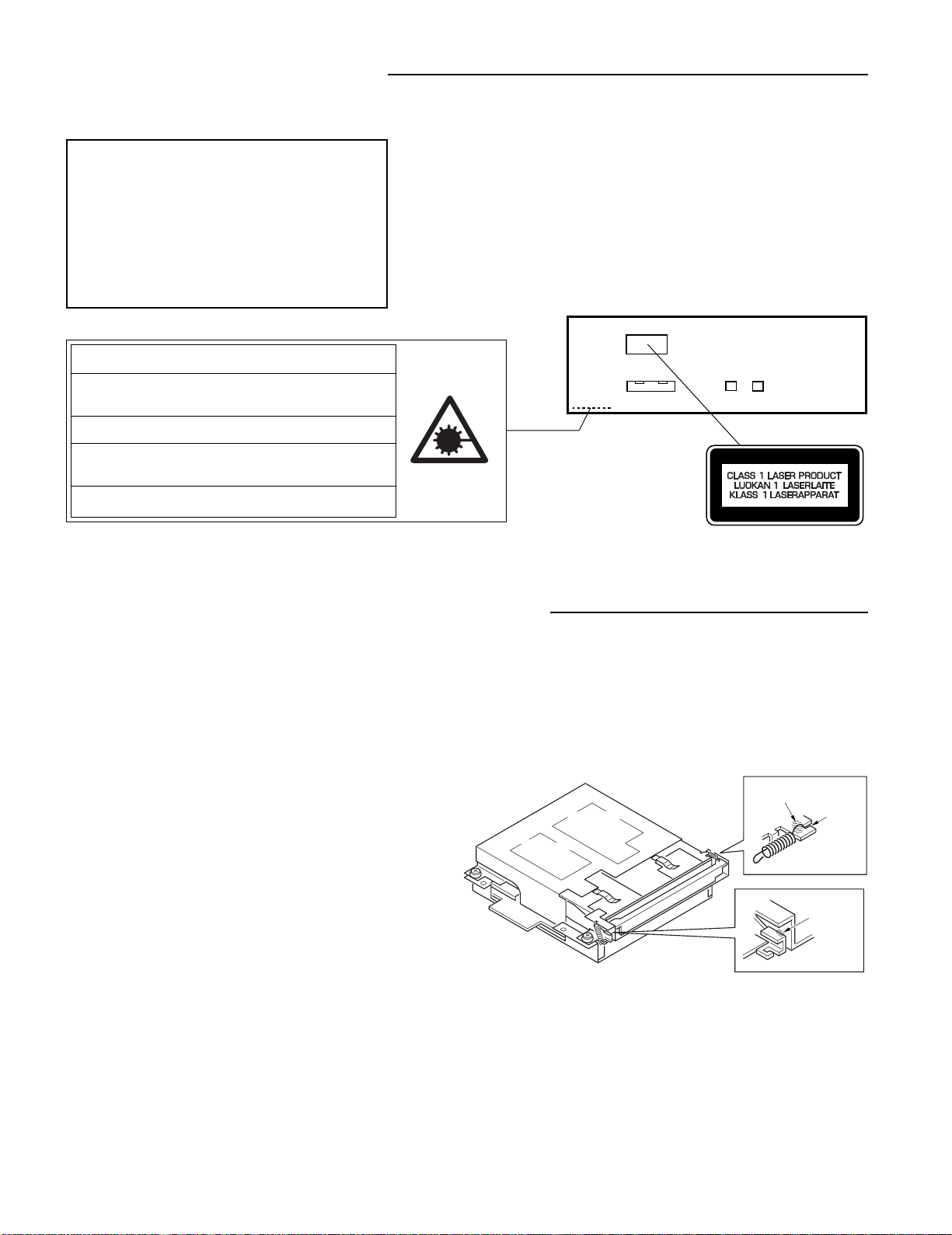
Sanyo MDG-X5 User manual

FILE NO.
Service Manual
Specifications
Separate Mini Component System
MD Deck MDG-X5 (UK)
MDG-077 (XE)
PRODUCT CODE No.
137 088 08 (UK)
137 088 09 (XE)
REFERENCE No. SM5810170
E O E C N RO ER B0 7
ON
L EP
R CM TE
A Em
M m
D E T
M P YM DE
T PE T PEMD
D C S E T
DkCD
M
90
+0+0
E
S RO L
D O
U O A ER
D P YM E
CM D
n
f
d
Sampling frequency ......... 44.1 kHz
Laser output ..................... 7.04mW(Continuos wave max.)
Wave length ..................... 785mm
Wow/flutter ....................... Below measurable limits
Recording system ............ Magnetic modulation over write
Input/Output ..................... OPTICAL DIGITAL IN/OUT : Optical
Power supply ................... Supplied from the Tuner/Amplifier
Dimensions ...................... 270 (W) x 87 (H) x 285 (D) mm
Weight .............................. 2.3 kg
Specifications subject to change without notice.

- 1 -
LASER BAEM SAFETY PRECAUTION
• Pick-up that emits a laser beam is used in this CD player section.
CAUTION :
USE OF CONTROLS OR ADJUSTMENTS
OR PERFORMANCE OF PROCEDURES
OTHER THAN THOSE SPECIFIED HEREIN
MAY RESULT IN HAZARDOUS RADIATION
EXPOSURE
LASER OUTPUT..........0.6 mW Max. (CW)
WAVE LENGTH........... 790 nm
SYSTEM CONNECTOR
OPTICAL D G TAL
OUT
N
CAUTION – NVISIBLE LASER RADIATION WHEN OPEN AND
INTERLOCKS DEFEATED. AVOID EXPOSURE TO BEAM.
ADVARSEL – USYNLIG LASER STRÅLING VED ÅBNING, NÅR
S KKERHEDSAFBRYDERE ER UDE AF FUNKTION, UNDGÅ UDS ÆTTELSE
FOR STRÅL NG.
VARN NG – OSYNLIG LASER STRÅLNING NÄR DENNA DEL ÄR ÖPPNAD
OCH SPÄRR ÄR URKOPPLAD. STRÅLEN ÄR FARLIG.
VORSICHT – UNSICHTBARE LASERSTRAHLUNG TRITT AUS, WENN
DECKEL GEÖFFNET UND WENN SICHERHEITSVERR EGELUNG
ÜBERBRÜCKT IST. NICHT, DEM STRAHL AUSSETZEN.
VARO – AVATTAESSA JA SUOJALUKITUS OHITETTAESSA OLET ALTTIINA
NÄKYMÄTTÖMÄLLE LASERSÄTE LYLLE. ÄLÄ KATSO SÄTEESEEN.
(MD DECK)
REPLACEMENT AND LUBRICATION OF THE MD DOOR
TB1401B
EM-30LG
HOOK
Remove it from, and is a method MD door
1. A point of a coil(Front right side) is pinched with
tweezers, and it is taken off a hole of MD door.
A spring turns then, and seem not to be exhausted.
2. A ditch of a door is to be pushed from face, and MD
door is taken off an axis.
3. MD door axis is avoided.
MD door installation method
1. Put molykote (EM-30LG) on door contact department.
2. Fit turns an axis into ditch 2 places of MD door after
installing door shaft, and install it with care in
installation direction.
3. Pinch a point of coil spring with tweezers, and hang it
on a hole of a door.
(XE)

- 2 -
11
Y04
Y04
Y04
Y04
Y04
15
14
(75)
Y01
Y01
Y03
Y03
Y03
Y03
Y01
1
2
3
4
5
6
78
9
12
10
13
71 72
73
74
51
MM03
MM02
MM01
MM00
16
Y06 Y06
Y06
Y07 Y07
Y08
Y09
Y09
Y02
Y02
Y05
52
53
75
76
54
54 54
54
54
77
EXPLODED VIEW (CABINET,CHASSIS & MD MECHANISM)

- 3 -
PARTS LIST PRODUCT SAFETY NOTICE
EACH PRECAUTION IN THIS MANUAL SHOULD BE FOLLOWED DURING SERVICING. COMPONENTS IDENTIFIED WITH THE IEC
SYMBOL !
!IN THE PARTS LIST AND THE SCHEMATIC DIAGRAM DESIGNATED COMPONENTS IN WHICH SAFETY CAN BE OF
SPECIAL SIGNIFICANCE. WHEN REPLACING A COMPONENT IDENTIFIED BY !, USE ONLY THE REPLACEMENT PARTS DESIGNATED,
OR PARTS WITH THE SAME RATINGS OF RESISTANCE, WATTAGE OR VOLTAGE THAT ARE DESIGNATED IN THE PARTS LIST
IN THIS MANUAL. LEAKAGE-CURRENT OR RESISTANCE MEASUREMENTS MUST BE MADE TO DETERMINE THAT EXPOSED
PARTS ARE ACCEPTABLY INSULATED FROM THE SUPPLY CIRCUIT BEFORE RETURNING THE PRODUCT TO THE CUSTOMER.
CAUTION :Regular type resistors and capacitors are not listed. To know those values, refer to the schematic diagram.
Regular type resistors are less than 1/4 W carbon type and 0 ohm chip resistors.
Regular type capacitors are less than 50 V and less than 1000 µF type of Ceramic type and Electrical type.
PACKING & ACCESSORIES
REF.NO. PART NO. DESCRIPTION
614 305 2135 CARTON CASE,INNER (DC-X5/UK)
614 305 2142 CARTON CASE,INNER (DC-077/XE)
614 302 0752 CUSHION,FRONT,FRONT
614 302 0769 CUSHION,BACK,BACK
645 036 4334 POLY SHEET-0750X0400*NC,
SET (DC-X5/UK)
645 036 4341 POLY SHEET-0750X0400*NC,
SET (DC-077/XE)
645 036 9643 CABLE,OPTICAL
614 302 5306 INSTRUCTION MANUAL (UK)
614 303 9822 INSTRUCTION MANUAL (XE)
614 307 0603 INSTRUCTION MANUAL,GREEK (XE)
CABINET & CHASSIS
REF.NO. PART NO. DESCRIPTION
1 614 302 8468 ASSY,CABINET,FRONT
2 614 305 1114 ASSY,DEC MD
3 614 302 4361 KNOB,ROTARY,JOG
4 614 302 4248 BUTTON,EJECT,OPEN/CLOSE
5 614 302 0530 DEC,WINDOW LED,PLAY COMPU REC
6 614 302 4255 BUTTON,EDIT
7 614 303 7330 BUTTON,PLAY,PLAY/PAUSE
8 614 302 4354 HOLDER,LED,COMPU REC
9 614 302 9687 REFLECTOR,LED,LEFT
10 614 302 4415 REFLECTOR,LED,RIGHT
11 614 304 7834 ASSY,CABINET,AFTER BENDING
12 614 303 6432 DEC,SHEET,LED,LEFT
13 614 302 4330 DEC,SHEET,LED,RIGHT
14 614 302 8956 ASSY,CABINET,BOTTOM
15 614 302 4385 PANEL,REAR,REAR (UK)
15 614 304 0057 PANEL,REAR,REAR (XE)
16 614 302 4378 MOUNTING,MD,MECHA
614 274 8190 LABEL,SAFETY,LASER
FIXING PARTS
REF.NO. PART NO. DESCRIPTION
Y01 411 021 3503 SCR S-TPG BIN 3X10,
FRONT-BOTTOM FIX
Y02 411 021 3701 SCR S-TPG BIN 3X10,
REAR-ELECT PART
Y03 411 021 3503 SCR S-TPG BIN 3X10,FRONT PWB FIX
Y04 411 021 3701 SCR S-TPG BIN 3X10,CABINET
Y05 411 021 3701 SCR S-TPG BIN 3X10,BOTTOM-REAR
Y06 411 023 4003 SCR S-TPG PAN 3X10,MD MECHA
Y07 411 021 3503 SCR S-TPG BIN 3X10,
MOUNTING-BOTTOM
Y08 411 020 9902 SCR S-TPG BRZ+FLG 3X8,TRANS
Y09 411 021 3503 SCR S-TPG BIN 3X10,MAIN PWB
ELECTRICAL PARTS
REF.NO. PART NO. DESCRIPTION
51 645 036 9650 FLEXIBLE FLAT CABLE,
MECHA-FRONT PWB
52 645 037 3190 FLEXIBLE FLAT CABLE,
MECHA-POWER SUPPLY PWB
53 !
!! 645 034 8020 TRANS,POWER
54 614 129 9082 LUG
MD SWITCH P.W.BOARD ASSY
REF.NO. PART NO. DESCRIPTION
71 614 303 3851 ASSY,PWB,MD SW(Only Initial)
CN543 614 035 4911 SOCKET,DIP 2P
or 614 237 9752 SOCKET
S5430 645 006 5958 SWITCH,PUSH 1P-1T
or 614 220 5471 SWITCH,TACT
or 614 240 1002 SWITCH,TACT
S5431 645 006 5958 SWITCH,PUSH 1P-1T
or 614 220 5471 SWITCH,TACT
or 614 240 1002 SWITCH,TACT
MD FRONT P.W.BOARD ASSY
REF.NO. PART NO. DESCRIPTION
72 614 302 6792 ASSY,PWB,MD FRONT (Only Initial)
CN530 614 303 1550 ASSY,WIRE
CN531 614 302 4231 ASSY,WIRE
CN532 645 034 8631 SOCKET,FPC 23P
CN533 614 035 4911 SOCKET,DIP 2P
or 614 237 9752 SOCKET
CN534 614 035 4911 SOCKET,DIP 2P
or 614 237 9752 SOCKET
CN535 614 035 4911 SOCKET,DIP 2P
or 614 237 9752 SOCKET
D5301 408 037 4204 LED SLP-3118B-51HAB-T1
D5302 408 032 5404 LED SLP-9118C-51H-S-T1
FL501 645 034 8044 FLOURESCENT TUBE
HL530 614 302 4347 HOLDER,FL,HOLDER-FL
IC531 410 342 8303 IC M38197MAA-625FP
IC532 409 427 7805 IC TC74ACT32FT
L5961 645 001 4550 INDUCTOR,10U K
or 645 031 7835 INDUCTOR,10U K
L5962 645 001 4550 INDUCTOR,10U K
or 645 031 7835 INDUCTOR,10U K
Q5301 405 000 3400 TR DTC114TS
or 405 109 9402 TR KRC111M
Q5302 405 000 3400 TR DTC114TS
or 405 109 9402 TR KRC111M
Q5303 405 143 8706 TR KTC3199-GR
or 405 017 9600 TR 2SC3330-T
or 405 017 9709 TR 2SC3330-U
or 405 011 8500 TR 2SC1740S-R
or 405 011 8609 TR 2SC1740S-S

- 4 -
PARTS LIST
REF.NO. PART NO. DESCRIPTION
Q5304 405 000 6104 TR DTC144ES
or 405 146 1209 TR KRC104M
Q5305 405 000 2205 TR DTA144ES
or 405 146 1308 TR KRA104M
Q5330 405 075 8102 TR DTA143ZS
or 405 143 8904 TR KRA106M
RA531 614 218 0525 RESISTOR
S5301 645 034 8037 SWITCH,ROTARY(ENCODER)
S5302 645 006 5958 SWITCH,PUSH 1P-1T
or 614 220 5471 SWITCH,TACT
or 614 240 1002 SWITCH,TACT
S5304 645 006 5958 SWITCH,PUSH 1P-1T
or 614 220 5471 SWITCH,TACT
or 614 240 1002 SWITCH,TACT
S5305 645 006 5958 SWITCH,PUSH 1P-1T
or 614 220 5471 SWITCH,TACT
or 614 240 1002 SWITCH,TACT
S5306 645 006 5958 SWITCH,PUSH 1P-1T
or 614 220 5471 SWITCH,TACT
or 614 240 1002 SWITCH,TACT
S5308 645 006 5958 SWITCH,PUSH 1P-1T
or 614 220 5471 SWITCH,TACT
or 614 240 1002 SWITCH,TACT
S5309 645 006 5958 SWITCH,PUSH 1P-1T
or 614 220 5471 SWITCH,TACT
or 614 240 1002 SWITCH,TACT
S5310 645 006 5958 SWITCH,PUSH 1P-1T
or 614 220 5471 SWITCH,TACT
or 614 240 1002 SWITCH,TACT
S5311 645 006 5958 SWITCH,PUSH 1P-1T
or 614 220 5471 SWITCH,TACT
or 614 240 1002 SWITCH,TACT
S5312 645 006 5958 SWITCH,PUSH 1P-1T
or 614 220 5471 SWITCH,TACT
or 614 240 1002 SWITCH,TACT
S5313 645 006 5958 SWITCH,PUSH 1P-1T
or 614 220 5471 SWITCH,TACT
or 614 240 1002 SWITCH,TACT
X5301 645 027 5470 OSC,CERAMIC 8MHZ
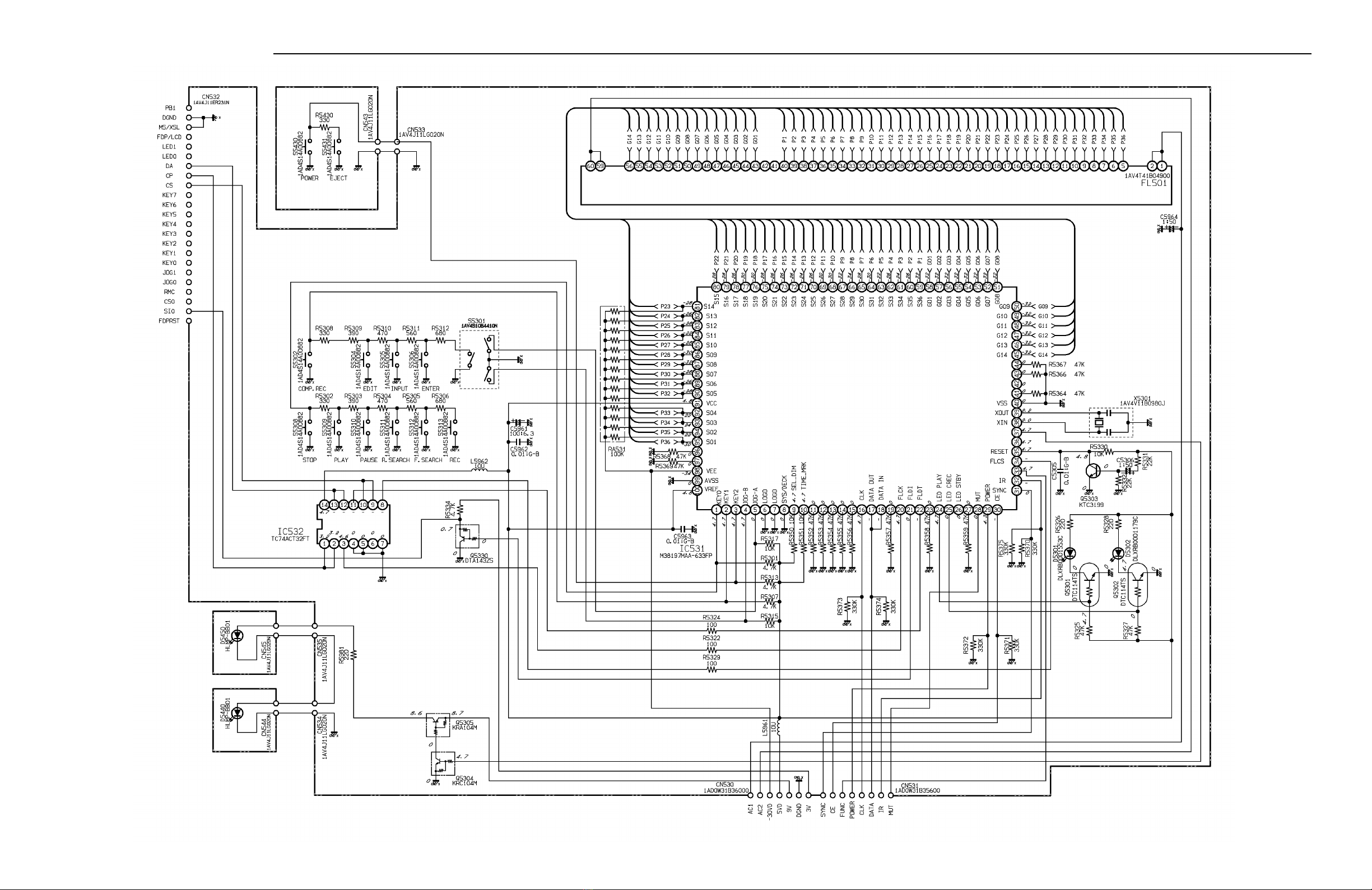
MD LED2 P.W.BOARD ASSY
REF.NO. PART NO. DESCRIPTION
73 614 303 3875 ASSY,PWB,MD LED2 (Only Initial)
CN545 614 035 4911 SOCKET,DIP 2P
or 614 237 9752 SOCKET
D5450 407 212 8907 LED HLMP-BB01-J0B00
MD LED1 P.W.BOARD ASSY
REF.NO. PART NO. DESCRIPTION
74 614 303 3868 ASSY,PWB,MD LED1 (Only Initial)
CN544 614 035 4911 SOCKET,DIP 2P
or 614 237 9752 SOCKET
D5440 407 212 8907 LED HLMP-BB01-J0B00
MD POWER SUPPLY P.W.BOARD ASSY
REF.NO. PART NO. DESCRIPTION
75 614 302 6808 ASSY,PWB,MD POWER SUPPLY
(Only Initial)
C5021 403 057 0007 POLYESTER 0.01U J 50V
C5905 403 329 6003 ELECT 4700U M 25V
CN500 645 005 8134 PLUG,8P
CN501 645 006 0861 PLUG,7P
CN502 614 239 5455 SOCKET
CN503 645 035 5769 SOCKET,FPC 26P
CN572 407 212 5708 PHOTO COUPLE GP1F38R
CN573 407 212 8709 PHOTO COUPLE TOTX140
or 407 210 0408 PC PHOTO COUPLE GP1F38T
CN591 614 020 6548 SOCKET,2P
or 614 223 9209 SOCKET
CN592 614 020 6586 SOCKET,6P
D5901 !
!407 148 6701 DIODE 1A3-I
D5902 !
!407 148 6701 DIODE 1A3-I
D5903 !
!407 148 6701 DIODE 1A3-I
D5904 !
!407 148 6701 DIODE 1A3-I
D5931 !
!407 148 6701 DIODE 1A3-I
D5932 407 100 0303 ZENER DIODE MTZJ36B
D5933 407 063 9108 ZENER DIODE MTZJ6.8B
HS501 614 264 0159 HEAT SINK
IC503 409 185 6102 IC TC74HCU04AP
IC571 409 384 3506 IC BA3314F
IC572 409 426 1804 IC KIA4558S
IC573 409 333 2505 IC BU4066BCF
IC592 409 453 5400 IC NJM2930L85
IC593 409 382 0309 IC LA5620
L5701 645 001 4581 INDUCTOR,100U K
or 645 031 7842 INDUCTOR,100U K
L5801 645 001 4581 INDUCTOR,100U K
or 645 031 7842 INDUCTOR,100U K
L5901 645 001 4550 INDUCTOR,10U K
or 645 031 7835 INDUCTOR,10U K
L5902 645 001 4581 INDUCTOR,100U K
or 645 031 7842 INDUCTOR,100U K
L5903 645 006 3602 INDUCTOR,1.1UH
L5904 645 006 3602 INDUCTOR,1.1UH
L5905 645 006 3602 INDUCTOR,1.1UH
L5951 645 001 5519 INDUCTOR,47U K
LUG50 645 023 8987 FIXER,FIX_WIRE
LUG51 645 023 8987 FIXER,FIX_WIRE
PR591 !
!645 027 4169 PROTECTOR,0.125A 125V
Q5340 405 000 6104 TR DTC144ES
or 405 146 1209 TR KRC104M
Q5341 405 000 2205 TR DTA144ES
or 405 146 1308 TR KRA104M
Q5342 405 000 6104 TR DTC144ES
or 405 146 1209 TR KRC104M
Q5343 405 000 2205 TR DTA144ES
or 405 146 1308 TR KRA104M
Q5710 405 000 3400 TR DTC114TS
or 405 109 9402 TR KRC111M
Q5810 405 000 3400 TR DTC114TS
or 405 109 9402 TR KRC111M
Q5901 405 000 2205 TR DTA144ES
or 405 146 1308 TR KRA104M
Q5902 405 000 6104 TR DTC144ES
or 405 146 1209 TR KRC104M
Q5903 405 141 3505 TR KTA1266-Y
or 405 141 3406 TR KTA1266-GR
or 405 004 4502 TR 2SA608-F-NP
or 405 004 5004 TR 2SA608-G-NP
Q5904 405 143 8706 TR KTC3199-GR
or 405 017 9600 TR 2SC3330-T
or 405 017 9709 TR 2SC3330-U
or 405 011 8500 TR 2SC1740S-R
or 405 011 8609 TR 2SC1740S-S

- 5 -
MD MECHANISM (MDG007/SH)
REF.NO. PART NO. DESCRIPTION
MM00 614 304 8350 ASSY,MECHA,MDG007/SH,MD MECHA
MM01 614 303 8344 ASSY,DOOR,MD DOOR W/PAINTING
MM02 614 303 6609 SHAFT,DOOR,MD DOOR SHAFT
MM03 614 303 6616 SPRING,DOOR,MD DOOR RETURN
REF.NO. PART NO. DESCRIPTION
Q5905 405 007 3106 TR 2SB544-F-MP
or 405 007 2901 TR 2SB544-E-MP
Q5931 405 141 3505 TR KTA1266-Y
or 405 141 3406 TR KTA1266-GR
or 405 004 4502 TR 2SA608-F-NP
or 405 004 5004 TR 2SA608-G-NP
SA001 411 021 3503 SCR S-TPG BIN 3X10,FOR IC593
MD PT-SEC P.W.BOARD ASSY
REF.NO. PART NO. DESCRIPTION
77 614 302 6815 ASSY,PWB,MD PT-SEC (Only Initial)
CN599 614 020 6586 SOCKET,6P
PR599 !
!! 645 014 2550 PROTECTOR,2A 125V
MD PT-PRE P.W.BOARD ASSY
REF.NO. PART NO. DESCRIPTION
76 614 303 3882 ASSY,PWB,MD PT-PRE (Only Initial)
CN596 614 020 6548 SOCKET,2P
or 614 223 9209 SOCKET
L5960 614 213 5761 INDUCTOR,FERITE
PARTS LIST
FL DISPLAY & DESCRIPTION
B14 (13G)
(12G~1G)
B1 B13
B26
S1
S2
14G 12G 11G 10G 9G 8G 6G 5G7G 4G 3G 2G 1G 13G
1-7
1-1
1-2
1-3
1-4
1-5
1-6
2-7
2-1
2-2
2-3
2-4
2-5
2-6
3-7
3-1
3-2
3-3
3-4
3-5
3-6
4-7
4-1
4-2
4-3
4-4
4-5
4-6
5-7
5-1
5-2
5-3
5-4
5-5
5-6
PIN CONNECTION
PIN NO. 60 59 58 57 56 55 54 53 52 51 50 49 48 47 46 45 44 43 42 41
CONNECTION F2 F2 NP NP 14G 13G 12G 11G 10G 9G 8G 7G 6G 5G 4G 3G 2G 1G NC NC
PIN NO. 40 39 38 37 36 35 34 33 32 31 30 29 28 27 26 25 24 23 22 21
CONNECTION P1 P2 P3 P4 P5 P6 P7 P8 P9 P10 P11 P12 P13 P14 P15 P16 P17 P18 P19 P20
PIN NO. 20 19 18 17 16 15 14 13 12 11 10 987654321
CONNECTION P21 P22 P23 P24 P25 P26 P27 P28 P29 P30 P31 P32 P33 P34 P35 P36 NP NP F1 F1
NOTE: 1) F1,F2 ..... Filament 4) DL ........... Datum Line
2) NP ........... No pin 5) 1G〜14G Grid
3) NC ........... No connection

- 6 -
FL DISPLAY & DESCRIPTION
ANODE CONNECTION
14G 13G 12G 11G 10G 9G 8G 7G 6G 5G 4G 3G 2G 1G
P1 MONO DISC TRACK REMAIN CLOCK SLEEP
P2 1-1 1-1 1-1 1-1 1-1 1-1 1-1 1-1 1-1 1-1 1-1 1-1
P3 TOC B1 2-1 2-1 2-1 2-1 2-1 2-1 2-1 2-1 2-1 2-1 2-1 2-1
P4 EDIT B8 3-1 3-1 3-1 3-1 3-1 3-1 3-1 3-1 3-1 3-1 3-1 3-1
P5 S2 B14 4-1 4-1 4-1 4-1 4-1 4-1 4-1 4-1 4-1 4-1 4-1 4-1
P6 RANDOM B21 5-1 5-1 5-1 5-1 5-1 5-1 5-1 5-1 5-1 5-1 5-1 5-1
P7 RPROGRAM 1-2 1-2 1-2 1-2 1-2 1-2 1-2 1-2 1-2 1-2 1-2 1-2
P8 A.SPACE B21 2-2 2-2 2-2 2-2 2-2 2-2 2-2 2-2 2-2 2-2 2-2 2-2
P9 REPEAT B9 3-2 3-2 3-2 3-2 3-2 3-2 3-2 3-2 3-2 3-2 3-2 3-2
P10 1B15 4-2 4-2 4-2 4-2 4-2 4-2 4-2 4-2 4-2 4-2 4-2 4-2
P11 AB22 5-2 5-2 5-2 5-2 5-2 5-2 5-2 5-2 5-2 5-2 5-2 5-2
P12 K1-3 1-3 1-3 1-3 1-3 1-3 1-3 1-3 1-3 1-3 1-3 1-3
P13 B3 2-3 2-3 2-3 2-3 2-3 2-3 2-3 2-3 2-3 2-3 2-3 2-3
P14 SYNC B10 3-3 3-3 3-3 3-3 3-3 3-3 3-3 3-3 3-3 3-3 3-3 3-3
P15 TrMARK B16 4-3 4-3 4-3 4-3 4-3 4-3 4-3 4-3 4-3 4-3 4-3 4-3
P16 TlMARK B23 5-3 5-3 5-3 5-3 5-3 5-3 5-3 5-3 5-3 5-3 5-3 5-3
P17 1-4 1-4 1-4 1-4 1-4 1-4 1-4 1-4 1-4 1-4 1-4 1-4
P18 B4 2-4 2-4 2-4 2-4 2-4 2-4 2-4 2-4 2-4 2-4 2-4 2-4
P19 B11 3-4 3-4 3-4 3-4 3-4 3-4 3-4 3-4 3-4 3-4 3-4 3-4
P20 B17 4-4 4-4 4-4 4-4 4-4 4-4 4-4 4-4 4-4 4-4 4-4 4-4
P21 B24 5-4 5-4 5-4 5-4 5-4 5-4 5-4 5-4 5-4 5-4 5-4 5-4
P22 S1 1-5 1-5 1-5 1-5 1-5 1-5 1-5 1-5 1-5 1-5 1-5 1-5
P23 B5 2-5 2-5 2-5 2-5 2-5 2-5 2-5 2-5 2-5 2-5 2-5 2-5
P24 B12 3-5 3-5 3-5 3-5 3-5 3-5 3-5 3-5 3-5 3-5 3-5 3-5
P25 B18 4-5 4-5 4-5 4-5 4-5 4-5 4-5 4-5 4-5 4-5 4-5 4-5
P26 B25 5-5 5-5 5-5 5-5 5-5 5-5 5-5 5-5 5-5 5-5 5-5 5-5
P27 OVER 1-6 1-6 1-6 1-6 1-6 1-6 1-6 1-6 1-6 1-6 1-6 1-6
P28 B6 2-6 2-6 2-6 2-6 2-6 2-6 2-6 2-6 2-6 2-6 2-6 2-6
P29 B13 3-6 3-6 3-6 3-6 3-6 3-6 3-6 3-6 3-6 3-6 3-6 3-6
P30 B19 4-6 4-6 4-6 4-6 4-6 4-6 4-6 4-6 4-6 4-6 4-6 4-6
P31 B26 5-6 5-6 5-6 5-6 5-6 5-6 5-6 5-6 5-6 5-6 5-6 5-6
P32 DIGITAL 1-7 1-7 1-7 1-7 1-7 1-7 1-7 1-7 1-7 1-7 1-7 1-7
P33 B7 2-7 2-7 2-7 2-7 2-7 2-7 2-7 2-7 2-7 2-7 2-7 2-7
P34 ANALOG 3-7 3-7 3-7 3-7 3-7 3-7 3-7 3-7 3-7 3-7 3-7 3-7
P35 B20 4-7 4-7 4-7 4-7 4-7 4-7 4-7 4-7 4-7 4-7 4-7 4-7
P36 STEREO 5-7 5-7 5-7 5-7 5-7 5-7 5-7 5-7 5-7 5-7 5-7 5-7
RE
C
IC BLOCK DIAGRAM & DESCRIPTION
IC503 TC74HCU04AP (HEX INVERTER)
1
2
3
4
5
6
78
9
10
11
12
13
14 V
CC
GND
6A
3A
3Y
6Y
1A
5A
4Y
1Y
5Y
4A
2A
2Y
IC532 TC74ACT32FT (Serial EEPROM)
1A
1B
1Y
2A
2B
2Y
GND
Vcc
4B
4Y
4A
3B
3A
3Y
1
2
3
4
5
6
7
14
13
12
11
10
9
8

- 7 -
IC BLOCK DIAGRAM & DESCRIPTION
IC571 BA3314F (Dula Preamplifier with ALC Detector) IC572 KIA4558S (Dula Low Noise Operational Amp.)
AB
OUT A
OUT B
-IN A
+IN A
VEE
VCC
VCC
+IN B
-IN B
123456789
IC573 BU4066BCF (Quad Analog Switch)
1
2
3
4
5
6
78
9
10
11
12
13
14 VCC
VSS
C1
C2
C3
C4
I/O1
I/O4
I/O3
O/I1
O/I4
O/I3
O/I2
I/O2
OUT/IN IN/OUT
SWA
IN/OUT OUT/IN
SWB
SWC
IN/OUT OUT/IN
SWD
OUT/IN IN/OUT
IC593 LA5620 (Multi Voltage System Regulator)
DELAY
CIRCUIT
DELAY
CIRCUIT
9
8
2
7
12
11
10
5
4
6
3
1
V
CC
PH5
B.BAK
ANA5
SYS3.3
GND
CD2
S.RESET
AC
STBY
CD1
P.DOWN

- 9 -- 8 -
SCHEMATIC DIAGRAM (FRONT)
This is a basic schematic diagram.

- 11 -- 10 -
PRODUCT SAFETY NOTICE
Each precaution in this manual should be followed during servicing. Components identified with the IEC symbol !! in the parts list and the schematic diagram
designated components in which safety can be of special significance. When replacing a component identified by !
!, use only the replacement parts
designated, or parts with the same ratings of resistance, wattage or voltage that are designated in the parts list in this manual. Leakage-current or resistance
measurements must be made to determine that exposed parts are acceptably insulated from the supply circuit before returning the product to the customer.
SCHEMATIC DIAGRAM (MAIN)
This is a basic schematic diagram.

- 13 -- 12 -
CN534
CN544 CN545
CN535
CN533
CN531
CN530
CN543
CN503
CN592
CN501
CN599
CN596
CN532
MD MECHANISM
MD LED1 P.W.B MD LED2 P.W.B
MD FRONT P.W.B
POWER SWITCH
P.W.B
MD POWER SUPPLY P.W.B
MD PT-SEC
P.W.B
MD PT-PRE
P.W.B
CN591
CN500
PT591
WIRING DIAGRAM

- 14 -
IC BLOCK DIAGRAM & DESCRIPTION
ROM RAN
P4(8)
P1(8)P0(8) P2(8)
Timer 1(8)
Timer 2(8)
Timer 3(8)
Timer 4(8)
Timer 5(8)
Timer 6(8)
3938
P4
4
/INT
4
P4
5
/INT
1
/ZCR
P4
7
/T3
OUT
P4
6
/T1
OUT
P4
3
/INT
3
P4
2
/INT
2
P4
1
P4
0
/INT
0
AV
SS
V
REF
27 28 29 30 31 32 33 34
P5(8)
11 12 13 14 17 18
15 16
P6(8)
19 20 21 22 23 24 25 26
P7(8)
123456799
100
8
P8(8)
81 82 83 84 85 86 87 88
P9(8)
73 74 75 76 77 78 79 80
48 47 46 45 4435 984091 43 42 41
56 55 54 53 52 51 50 49
64 63 62 61 60 59 58 57
PA(8)
89 90 92 93 94 95 96 97
P3
0
/SEG
24
P3
1
/SEG
25
P3
2
/SEG
26
P3
3
/SEG
27
PB(4)
10 36 37
P3
4
/SEG
28
P3
5
/SEG
29
P3
6
/SEG
30
P3
7
/SEG
31
P7
7
/AN
7
P8
7
/SEG
15
P8
6
/SEG
14
P8
5
/SEG
13
P8
4
/SEG
12
P8
3
/SEG
11
P8
2
/SEG
10
P8
1
/SEG
9
P8
0
/SEG
8
P9
7
/SEG
23
P9
6
/SEG
22
P9
5
/SEG
21
P9
4
/SEG
20
P9
3
/SEG
19
P9
2
/SEG
18
P9
1
/SEG
17
P9
0
/SEG
16
PA
7
/SEG
7
PA
6
/SEG
6
PA
5
/SEG
5
PA
4
/SEG
4
PB
2
/DA
9
PB
3
PB
1
/X
CIN
PB
0
/X
COUT
PA
3
/SEG
3
PA
2
/SEG
2
PA
1
/SEG
1
PA
0
/SEG
0
P7
6
/AN
6
P7
5
/AN
5
P7
4
/AN
4
P7
3
/AN
3
P7
2
/AN
2
P7
1
/AN
1
P7
0
/AN
0
P3(8)
65 66 67 68 69 70 71 72
S I/O1(8) S I/O2(8) S I/O3(8)
A-D
converter (8)
D-A
converter (8)
Local data
bus
T1
OUT
T3
OUT
PWM
CNTR
0
CNTR
1
A
X
Y
S
PC
L
PC
H
PS
CPU
Ciock generating
circuit
X
CIN
Sub-clock
input
X
COUT
Sub-clock
input
X
COUT
X
CIN
16
Zero cross
detection circuit
Interruqt interval
determination
circuit
INT
2
INT
3,
INT
4
INT
1
/
ZCR
SI/O
automatic
transfer
controller
SI/O
automatic
transfer RAM
controller
SI/O
automatic
display RAM
controller
FLD
automatic
display
controller
Data
P5
7
/S
RDY3
/AN
15
P5
6
/S
CLK3
/AN
14
P5
5
/S
OYT3
/AN
13
P5
4
/S
IN3
/AN
12
P5
3
/S
RDY2
/AN
11
P5
2
/S
CLK2
/AN
10
P5
1
/S
OUT2
/AN
9
P5
0
/S
IN2
/AN
8
P6
7
/S
RDY1
/CS/S
CLK12
P6
6
/S
CLK11
P6
5
/S
OUT1
P6
4
/S
IN1
P6
3
/CNTR
1
P6
2
/CNTR
0
P6
1
/PWM
P6
0
X
OUT
X
IN
RESET
V
CC
V
SS
V
EE
P0
0
/SEG
32
/DIG
0
P0
1
/SEG
33
/DIG
1
P0
2
/SEG
34
/DIG
2
P0
3
/SEG
35
/DIG
3
P0
4
/SEG
36
/DIG
4
P0
5
/SEG
37
/DIG
5
P0
6
/SEG
38
/DIG
6
P0
7
/SEG
39
/DIG
7
P1
0
/SEG
40
/DIG
8
P1
1
/SEG
41
/DIG
9
P1
2
/DIG
10
P1
3
/DIG
11
P1
4
/DIG
12
P1
5
/DIG
13
P1
6
/DIG
14
P1
7
/DIG
15
P2
0
/DIG
16
P2
1
/DIG
17
P2
2
/DIG
18
P2
3
/DIG
19
P2
4
P2
5
P2
6
P2
7
IC531 M38197MAA-636FP (Single Chip 8-bit C Mos)

SANYO Technosound Co., Ltd.
Osaka, Japan
Oct. / '00 / 2000 BB Printed in Japan
IC BLOCK DIAGRAM & DESCRIPTION
Pin Name Function
1P7
7
/AN
7
2P7
6
/AN
6
3P7
5
/AN
5
8-bit C MOS I/O port with the same functio
n
4P7
4
/AN
4
as ports P2
4
- P2
7
5P7
3
/AN
3
C MOS compatible input level
6P7
2
/AN
2
C MOS 3-state output
7P7
1
/AN
1
8P7
0
/AN
0
9PB
3
4-bit C MOS I/O port with the same functio
n
as ports P2
4
- P2
7
10 PB
2
/DA C MOS compatible input level
C MOS 3-state output
11 P5
7
/S
RDY3
/AN
15
12 P5
6
/S
CLK3
/AN
14
13 P5
5
/S
OUT3
/AN
13
14 P5
4
/S
IN3
/AN
12
15 P5
3
/S
RDY2
/AN
11
8-bit C MOS I/O port with the same functio
n
16 P5
2
/S
CLK2
/AN
10
as ports P2
4
- P2
7
17 P5
1
/S
OUT2
/AN
9
C MOS compatible input level
18 P5
0
/S
IN2
/AN
8
C MOS 3-state output
19 P6
7
/S
RDY1
/CS/S
CLK12
20 P6
6
/S
CLK11
21 P6
5
/S
OUT1
22 P6
4
/S
IN1
23 P6
3
/CNTR
1
24 P6
2
/CNTR
0
25 P6
1
/PWM
26 P6
0
27 P4
7
/T3
OUT
6-bit C MOS I/O port with the same functio
n
as ports P2
4
- P2
7
28 P4
6
/T1
OUT
C MOS compatible input level
C MOS 3-state output
29 P4
5
/INT
1
/ZCR 2-bit input port
C MOS compatible input level
30 P4
4
/INT
4
6-bit C MOS I/O port with the same functio
n
31 P4
3
/INT
3
as ports P2
4
- P2
7
32 P4
2
/INT
2
C MOS compatible input level
33 P4
1
C MOS 3-state output
34 P4
0
/INT
0
2-bit input port
C MOS compatible input level
35 RESET Reset input pin for active "L"
36 PB
1
/X
CIN
4-bit C MOS I/O port with the same functio
n
as ports P2
4
- P2
7
37 PB
0
/X
OUT
C MOS compatible input level
C MOS 3-state output
Input and output pins for the main clock
generating circuit.
Feedback resistor is built in between XIN
pin and Xout pin.
38 X
IN
Connect a ceramic resonator or a quartz-
crystal oscillator between the X
IN
pin and
X
OUT
pin to set oscillation frequency.
39 X
OUT
If an external clock is used, connect the
clock source to the X
IN
pin and leave the
X
OUT
pin open.
This clock is used as the oscillating source
of system clock.
40 V
SS
Apply voltage of 0V to V
SS
41 P2
7
4-bit I/O port
42 P2
6
I/O direction register allows each pin to
individually programmed as either input or
output.
43 P2
5
At reset this port is set to input mode.
44 P2
4
TTL input level
C MOS 3-state output
Pin Name Function
45 P2
3
/DIG
19
46 P2
2
/DIG
18
4-bit output port with the same function as port P0
47 P2
1
/DIG
17
48 P2
0
/DIG
16
49 P1
7
/DIG
15
50 P1
6
/DIG
14
51 P1
5
/DIG
13
52 P1
4
/DIG
12
8-bit output port with the same function as port P0
53 P1
3
/DIG
11
54 P1
2
/DIG
10
55 P1
1
/SEG
41
/DIG
9
56 P1
0
/SEG
40
/DIG
8
57 P0
7
/SEG
39
/DIG
7
58 P0
6
/SEG
38
/DIG
6
8-bit output port
59 P0
5
/SEG
37
/DIG
5
This port builds in pull-down resistor between
60 P0
4
/SEG
36
/DIG
4
port P0 and the V
EE
pin
61 P0
3
/SEG
35
/DIG
3
At reset this port is set to V
EE
level
62 P0
2
/SEG
34
/DIG
2
The high-breakdown-voltage P-channel open-
63 P0
1
/SEG
33
/DIG
1
drain
64 P0
0
/SEG
32
/DIG
0
65 P3
7
/SEG
31
66 P3
6
/SEG
30
67 P3
5
/SEG
29
68 P3
4
/SEG
28
8-bit output port with the same function as port P0
69 P3
3
/SEG
27
70 P3
2
/SEG
26
71 P3
1
/SEG
25
72 P3
0
/SEG
24
73 P9
7
/SEG
23
74 P9
6
/SEG
22
75 P9
5
/SEG
21
76 P9
4
/SEG
20
8-bit output port with the same function as port P0
77 P9
3
/SEG
19
78 P9
2
/SEG
18
79 P9
1
/SEG
17
80 P9
0
/SEG
16
81 P8
7
/SEG
15
82 P8
6
/SEG
14
83 P8
5
/SEG
13
8-bit I/O port with the same function as ports
84 P8
4
/SEG
12
P2
4
-P2
7
85 P8
3
/SEG
11
C MOS compatible input level
86 P8
2
/SEG
10
The high-breakdown-voltage P-channel open-
87 P8
1
/SEG
9
drain
88 P8
0
/SEG
8
89 PA
7
/SEG
7
90 PA
6
/SEG
6
91 V
CC
Apply voltage of 4.0 to 5.5V to V
CC
92 PA
5
/SEG
5
8-bit I/O port with the same function as ports
93 PA
4
/SEG
4
P2
4
-P2
7
94 PA
3
/SEG
3
C MOS compatible input level
95 PA
2
/SEG
2
The high-breakdown-voltage P-channel open-
96 PA
1
/SEG
1
drain
97 PA
0
/SEG
0
98 V
EE
Applies voltage supplied to pull-down resistors
of ports P0, P1, P2
0
-P2
3
, P3 and P9
GND input pin for A-D converter and D-A converter
Connect AV
SS
to V
SS
Reference voltage input pin for A-D converter and
D-A converter
99 AV
SS
V
REF
100
This manual suits for next models
1
Table of contents
Other Sanyo Stereo System manuals

Sanyo
Sanyo DC-BM300 User manual

Sanyo
Sanyo G-2915NK User manual

Sanyo
Sanyo DC-D3 User manual

Sanyo
Sanyo DC-DA2000 User manual

Sanyo
Sanyo DC-PT80 User manual

Sanyo
Sanyo DC-X850 User manual

Sanyo
Sanyo Dc-MS5 User manual

Sanyo
Sanyo DC-DA90 User manual

Sanyo
Sanyo DC-F190 User manual

Sanyo
Sanyo DC-C30 User manual