Sanyo CE28CH3-C User manual

Service Manual
Colour Television
Part No. SKSM0539 C5WHV MARCH 2002
Model CE28CH3-C
Service Ref. No. CE28CH3-C-00
PRODUCT CODE: 111361007
ORIGINAL VERSION: Chassis HA2A
Give complete “SERVICE REF. NO.” for parts
order or servicing. It is shown on the rating
plate at the cabinet back of the unit.
This T.V. receiver will not work properly in
foreign countries where the television
transmission system and power source
differ from the design specifications. Refer
to the specification table.
CE28CH3-C
CONTENTS
Safety precautions/Specifications..........................................................................................................2
Block Diagrams..................................................................................................................................3 -9
Cabinet Disassembly ..........................................................................................................................10
Adjustment and Repair Procedures..............................................................................................11 - 15
CPU Functions..............................................................................................................................16 - 17
IC block diagrams ........................................................................................................................18 - 22
Pin description of semi-conductors......................................................................................................23
Parts description and reading of schematic diagram ..........................................................................24
Cabinet Parts List/TV Stand Parts List ................................................................................................25
Electrical Parts List........................................................................................................................26- 37
Please use Circuit Diagram SKP20352 with this
service manual

C5WHV
1: An isolation transformer should be connected in the
power line between the receiver and the AC line
when a service is performed on the primary of the
converter transformer of the set.
2: Comply with all caution and safety-related notes
provided on the cabinet back, inside the cabinet, on
the chassis or the picture tube.
3: When replacing a chassis in the cabinet, always be
certain that all the protective devices are installed
properly, such as, control knobs, adjustment covers
or shields, barriers, isolation resistor-capacitor
networks etc.Before returning any television to the
customer, the service technician must be sure that it
is completely safe to operate without danger of
electrical shock.
2
SAFETY PRECAUTION
X-RADIATION PRECAUTION
The primary source of X-RADIATION in the television receiver is the picture tube. The picture tube is specially
constructed to limit X-RADIATION emissions. For continued X-RADIATION protection, the replacement tube must
be the same type as the original including suffix letter. Excessive high voltage may produce potentially hazardous
X-RADIATION. To avoid such hazards, the high voltage must be maintained within specified limit. Refer to this
service manual, high voltage adjustment for specific high voltage limit. If high voltage exceeds specified limits,
take necessary corrective action. Carefully follow the instructions for +B1 volt power supply adjustment, and high
voltage adjustment to maintain the high voltage within the specified limits.
PRODUCT SAFETY NOTICE
Product safety should be considered when a component replacement is made in any area of a receiver.
Components indicated by mark in the parts list and the schematic diagram designate components in which
safety can be of special significance. It is particularly recommended that only parts designated on the parts list in
this manual be used for component replacement designated by mark . No deviations from resistance wattage
or voltage ratings may be made for replacement items designated by mark .
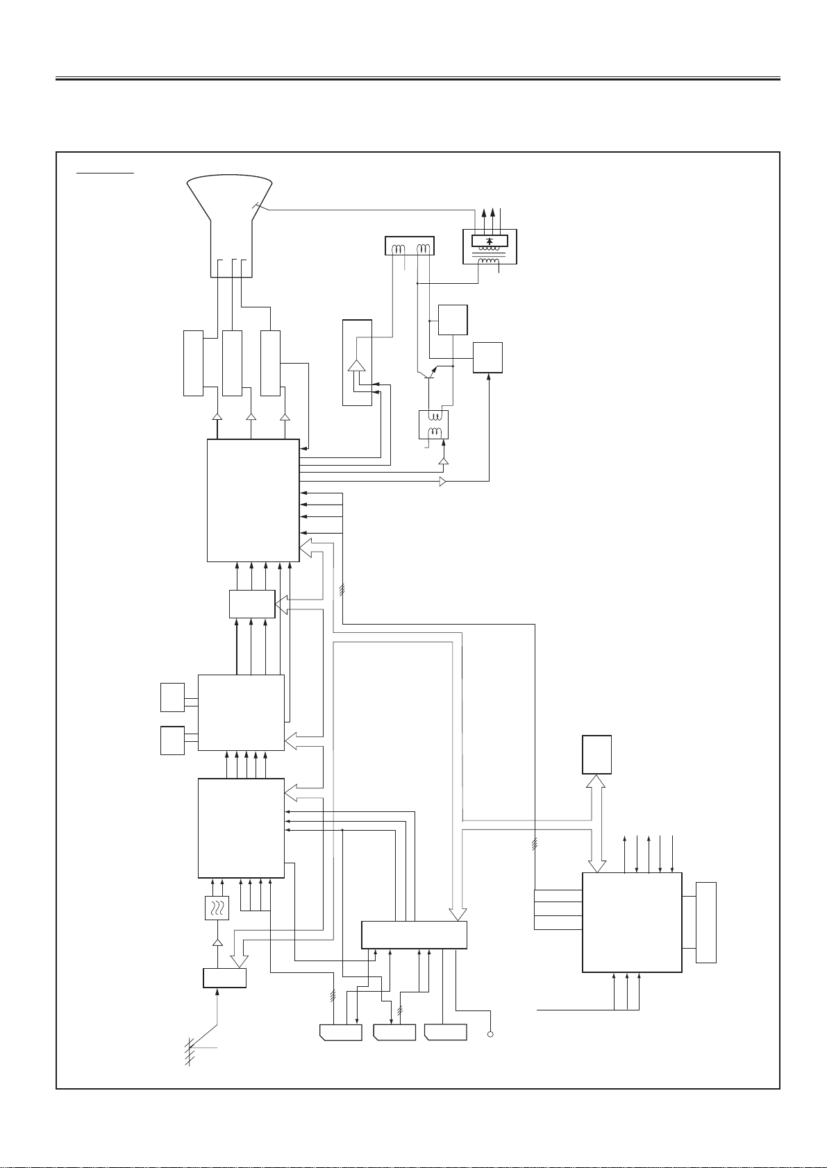
Power source AC 220~240V 50Hz
Television system System B/G
Colour system PAL/NTSC4.43 on air (NTSC3.58 in AV mode)
Channel coverage VHF: E2-E12
UHF: #21-#69
CATV: X, Y, Z.
Aerial input impedance 75ohm
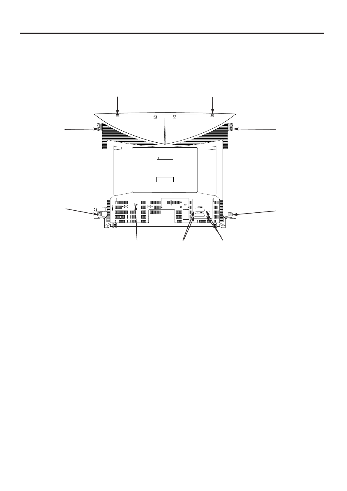
AV terminal
21-pin terminals AV1: CENELEC Standard with RGB
AV2: CENELEC Standard with S-inputs
Front AV terminals AV3: RCA Terminal, Video and Audio(L/R) Input
Sound output 10 x 2
Picture tubes(inches) 28”
Dimensions(WxHxD) 736 x 595.5 x 500mm
Weight 32.5 Kg
SPECIFICATIONS
!
!
!

3C5WHV
This is a basic diagram for all models and therefore differs slightly from the actual block diagram.
ROM
47
19
20
21
46 45 44 23
24
SCART1
AV1
SCART2
AV2
SCART3
AV3
FRONT
AV4
MONITOR-
OUT SC1 V-IN
SC3 V-IN
FRONT V-IN
23
41
1
9
11
27
13
34
37
39
19
20
SC2Y-IN
SC1-IN
POWER-ON
KEY-IN
MUTE
POWER FAIL DETECT IN
RC IN
SC2-IN
SC3-IN
SC2 C-IN
IC1201
MM1313BD
TV-OUT
R/G/B/BLK
SCL/SDA
IC101
<TDA9321H>
IF/VIDEO/
CHROMA/
MARTIX
2
3
36
37
38
39 34 18 20 21 47
61
60
51
50
49
46
CVBS-OUT
Y-OUT
C-OUT
CVBS-2-IN
R
G
B
BLK
IF
4
5
Aerial
Tuner X132
SAF
Q131
85
90
92
63
68
171 70
100
98
6
IC7201
<TC90A36FM>
SCAN
CONVERTER
Y
U
V
HD
VD
IC101
TDA9321
FIELD
MEMORY
IC7202
<MSM518221>
FIELD
MEMORY
IC7203
<MSM518221>
6
8
911 1416
17
19
2Y-OUT
2U-OUT
2V-OUT
IC241
<TDA9178>
IC351
<TDA9330H>
MATRIX
DEFLECTION
IC202
TDA9330
28
27
26
23
24 844
40
41
42
38 37 36 35 3
10 11
SDA/SCL
SCL/SDA
IC801
<ST92R195>
CPU
RGBBLK
OSD
BGR
BLK
IC711
TDA6101
IC721
TDA6101
IC731
TDA6101
BVIDEO-OUT
GVIDEO-OUT
RVIDEO-OUT
358
358
358
G
B
RCRT
IC501
<LA7876>
12
H-DRIVE
E-W
Q402
T401A
H-DRIVE
IK
Q271
Q272
Q273
G
R
B
V DRIVE -
V DIRVE+
PCC
CONTROL
CS
CONTROL
H-OUTPUT
Q411
FOCUS
SCREEM
T402
FLYBACK
V
H
D.Y
VERT
OUTPUT
653
Y
U
V
VD
HD
AV
SELECTOR
IC802
I2C BUS
2VD-OUT
2HD-OUT
MEMORY
SCL/SDA
Q381
TV-OUT H.V
IC871
2
+
_
Q471-Q461
From Scart
Outline
[Chassis Block Diagrams]
Fig.-1
CHASSIS DESCRIPTION

4
C5WHV
IC101
IF/VIDEO/
CHROMA
<TDA9321H>
IC351
MATRIX
<TDA9330H>
IC241
SHARPNESS
<TDA9178>
IC801
CPU
DIGITAL
SCAN
CONVERTER
CIRCUIT
AV
SELECTOR
CIRCUIT
SIF
Filtering
circuit
Buffer
2
3
10
12
13
14
18 20 21
34
36
|
38
61
60
23
40
41
42
38
30-38
24
49
50
51
6
8
9
19
17
16
26
27
28
Y, U, V 2(Y, U, V)
H-Sync
V-Sync
CVBS (TeleText)
2HD
2VD
External RGB in
(AV1 In)
SAW Filter
IF Stage
Video-in
C-in
Y-in
AV1
AV2
AV3
AV4
358
IC731
R-VIDEO OUT
<TDA6101Q>
358
IC721
G-VIDEO OUT
<TDA6101Q>
358
IC711
B-VIDEO OUT
<TDA6101Q>
R
G
B
IK
RGB OSD
DISPLAY from CPU
Picture Tube
Video signal rooting
SCART1
AV1
SCART2
AV2
SCART2
AV3
FRONT
AV4
L/R SC3-IN
IC1201
MM1313
42
41
2
4
8
10
14
16
33
32
IC3501
MM1369 3D
SURROUND
PROCESSOR
3D SUPPER
L
SPEAKER
R
SPEAKER
HEADPHONE
JACK
Q001
IC3451
TDA9875
Q3472
Q3471
L
R
23
1
10
9
13
11
6
40
39
12
1
25
26
IC001
TDA7263M AUDIO
AMP
8
310
15
MUTE
4
21
43
44
60
61
23
24 52
53
IC101
TDA9321
SCL/SDA
NICAM&
SOUND
CONTROLLER
L/R
TV-OUT
MONITOR
OUT SC1-IN
SC2-IN
L/R
Q1241
Q1242
Q1251
Q1252
FROM
CPU
L/R
TV-IN
SIF
MONO
Tuner Q131
X131
SAF
Aerial
L
RL
R
L/R
FRONT 4-IN 25
26
L/R
5
63
44
IF/VIDEO/
CHROMA
63
44 5
IF/VIDEO/
CHROMA
+
AV
SELECTOR
19
20
ACTIVE 3D SURROUND PROCESSING
46
47
Audio signal rooting
Fig.-2
Fig.-3
CHASSIS DESCRIPTION

5C5WHV
IC801
CPU
IC871
ROM
CVBS input
Q649
RL649
Power
Supply
Circuit
OSD
RGB Drive
H-Sync
V-Sync
1
|
5
63
|
80
61 60 48 49 44-47 43
37
25
RC Pre-amp.
I2C BUS
AV1 SW in
AV2 SW in
AV3 SW in
19 20 21 23 24
Key SW
Input
38 Power
Failuer
Detect
Power ON/OFF
DIGITAL
SCAN
CONVERTER
H-Drive
Q401-Q402 T401
Drive Trans
Q411
H-Output
IC501
V-Output <LA78476N>
56 3
V-Drive +
V-Drive -
3
8
2
1
23
24
EW-Out
Q471 Q461
Vert.
Coil
Horiz.
Coil
Deflection
Yoke
T402
FlyBack Trans.
L461/L462
Pcc Control
IC351
MATRIX
DEFLECTION
<TDA9330H>
2H-Sync
2V-Sync
L421
C421/C422
System control
Deflection circuit
Fig.-4
Fig.-5
CHASSIS DESCRIPTION

6
C5WHV
IC7202
Video Memory
IC7203
Video Memory
IC7204
PLL
<READ>
IC7201
DOUBLE SCAN CONVERTER
<TC90A36FM>
IC7205
PLL
<WRITE>
LPF
Q7301-Q7304
LPF
Q7311-Q7314
LPF
Q7321-Q7324
LPF
Q7371-Q7374
LPF
Q7361-Q7364
LPF
Q7351-Q7354
IC7341
Inverter
VD
HD
2VD
2HD
Y
U
V
2V
2U
2Y
12
85
90
92
100
98
6
10
5
14
6
11
13
31
|
50
9
|
31
717068635953
9
4
5
4
Digital scan circuit
100Hz Digital Scan Converter circuit
100Hz converter circuit consists of the following ICs.
- TC90A36F, IC7201
Field Progressive Converter
- MSM518221A, IC7202, IC7203
Video Memory
- TLC2932I, IC7205
PLL (Phase Locked Loop)
- MC74HC04AFP, IC7204
invertor
The Y-signal output from IC101 is sent to pin 85 of IC7201<TC90A36F>, field progressive
converter, after controlling the amplitude level and band-pass limiting by the circuit consist of
Q7301, Q7302, Q7303, Q7304 and 8MHz LPF. The U/V-signal are also controlling the amplitude
level and band-pass limiting by the circuit consist of Q7311, Q7312, Q7313, Q7314, Q7321,
Q7322, Q7323, Q7324 and 4MHz LPF respectively. The U-signal is sent to pin 90 of IC7201and
the V-signal is sent to pin 92 of IC7201. The HD signal is sent to pin 63 of IC7201 with positive
polarity through IC7341 for shaping the waveform. The VD-signal is sent to pin68 of IC7201 with
negative polarity through IC7341.
The Y-signal input to IC7201 is converted from A to D in 8bit and output from pins 18 to 25 of
IC7201 to pins 1 to 4 and 24 to 27 of IC7203<MSM51822A>, video memory, for writing.
[Digital Scan Operation]
Fig.-6
CHASSIS DESCRIPTION

7C5WHV
The U/V-signals are converted in progressive at multiplexer and converted from A to D in 8 bit,
and then applied from pins 34 to 41 of IC7201 to pins 1 to 40 and 24 to 27 of IC7203
<MSM518221A>, video memory, for writing.
The signals are wrote down to memory IC by 16MHz clock. It means the number of sampling are
1024 per 1H. The clock signal for writing is obtained by performing the phase comparing AFC
control to the HD-signal. The phase comparing AFC control performs at IC7205<TLC2932I>, PLL,
and IC7201. The 32MHz clock signal generated here is supplied from pin 3 of IC7205 and sent to
pin 61 of IC7201. The clock signal divided to 16MHz in the IC is output to pin 31 and supplied to
pins 6 of IC7202 and IC7203.
The reading is performed by 32MHz clock supplied from pin 28 of IC7201. In this case, the
number of sampling is 2048 per 1H. This read clock signal is obtained by performing the
frequency comparing AFC control to the input HD-signal. To avoid the skew distortion, the phase
comparing AFC control is not employed. The frequency comparing AFC control is performed at
IC7204<TLC2932I>, PLL, and IC7201. The 32MHz clock signal generated here is output from pin
3 of IC7205 and sent to pins 56 of IC7201 and IC7203.
The Y/U/V-signals are converted in progressive as the writing for 16MHz and reading for 32MHz.
The progressive V-signal output from pins 10 to 13 and 15 to 18 of IC7202 is supplied to pins 9 to
16. Also, the progressive U/V-signals output from pins 10 to 13 and 15 to 18 of IC7203 are
supplied to pins 43 to 50 of IC7201 and separated with U-signal and V-signal. And then, Y/U/V-
signals are converted in D to A in IC7201 and output to pin 6 as analogue Y-signal, pin 98 as
analogue V-signal and pin 100 as analogue V-signal respectively. The HD-signal progressive
converted in IC7201 is output from pin 71 of IC7201, the VD-signal progressive converted in
IC7202 is output from pin 70 of IC7201. The output HD and VD signals are sent to IC202 with
positive polarity through the IC7341 for waveform shaping.
The Y-signal output from IC7201 is controlled the amplitude level and band-pass limiting at the
circuit consist of Q7351, Q7352, Q7353, Q7354 and 16MHz LPF. The U/V-signals are also
controlled the amplitude level and band-pass limiting at the circuit consist of Q7361, Q7362,
Q7363, Q7364, Q7371, Q7372, Q7373, Q7374 and 8MHz LPF and these signals are sent to
IC201.
50Hz 100Hz
A
B
C
AA' BB' C
A' = A, B'= B
(a) Normal Scan (b) Double Scan
Fig.-7
CHASSIS DESCRIPTION

8
C5WHV
B-Y9
Y0Y1Y2Y3Y4
1H
1024 sampling
sampling clock= 16MHz = 1024/1 horiz.
Y0Y1Y2Y3Y4
R-Y0
B-Y0B-Y1B-Y2B-Y3B-Y4
R-Y4
R-Y3
R-Y2
R-Y1R-Y0B-Y1R-Y2B-Y3R-Y4
Write
Time divided multiplex
Y0Y1Y2Y3Y4
R-Y0B-Y1R-Y2B-Y3R-Y4
Y5Y6Y7Y8Y9
B-Y5R-Y6B-Y7 R-Y8
R-Y0
B-Y1
R-Y2
B-Y3
R-Y4R-Y4
B-Y5
R-Y6
B-Y7
R-Y8R-Y0
B-Y1B-Y3
R-Y2
B-Y7
R-Y6
B-Y9
R-Y8
B-Y5B-Y9
1H
2048 sampling
2048 sampling
Double
Scan
Converting
sampling clock = 32MHz = 2048/1 horiz.
Read out in double clock
(a) Write (b) Read
(c)
Fig.-8
CHASSIS DESCRIPTION

9C5WHV
5V Reg
5V Reg
5V Reg
CONVERTER TRANS
+
C609
Q613
OSC
Control
Rectifier
AC SW601
MAINS SW T681
RL649
RELAY
SW
5VRC
D681
Q611
D610 R641
IC631
30V
D637
D635
D3450
D634
D636
D633
D632
D631
Q649
IC651
8V
200V
T402
FLYBACK TRANS
HighVoltage
FocusVoltage
ScreenVoltage
CRT
Heater
D100
D7381
D651
D652
D1200
D856 D857
POWER ON/OFF
ON:HI
POWER ON
D459
19
10
2
4
D491
Video Out
Q411
Q853
Q851
Q852
2
3
1
8V Reg
18
17
16
15
14
13
11
10
3
2
8
5
T611
CPU
IC801
43
28 29
H-OUTPUT
130V Reg
35V
130V
-15V
IC652
12V
12V Reg
IC100
5V
IC3450
5V
IC7381
5V
9V
15V
Power Supply Lines
Power Failuer Detection Lines
12V Reg
IC681
IC1201
9V Reg
D456D457/D458
7.9V
High Voltage Detection
Power Failure detection
POWER FAILURE DETECTION
HOLD DOWN
Power supply & Protection circuit
Fig.-9
CHASSIS DESCRIPTION

10
C5WHV
DISASSEMBLY
CABINET BACK DISASSEMBLY
1. Remove 7 screws (A), 4 screws (B).
2. Pull out the cabinet back.
AV1
AV2
(A) (A)
(A)
(A)
(A)
(A)
(A) (B) (B)

11 C5WHV
SERVICE ADJUSTMENTS
[FEATURE SETTING]
To enter to the Feature Setting Mode
+ Press and hold the “GREEN” button (Remote control) and P▲button on the TV front control panel. The adjustment
window will appear on the screen.
+ Highlight the FEATURE menu by using the P▲or P▼button and then press the F/OK button. The window will
change to the feature setting window.
=>
To set the feature mode
+ Highlight the desired feature item by using the P▲or P▼button.
+ To change the feature mode, use the Volume - (LEFT) or Volume + (RIGHT) button.
+ The data which is set in the feature mode is stored into the memory IC automatically.
Following table shows the available feature items and default setting.
Exit from the Feature Setting Mode
+ Press the RECALL button on the remote control.
Feature items Mode Description & Note
ON-TIMER ON or OFF On-timer available, default “ON”
SORT MODE ATS EURO PLUS Tuning mode, default “ATS EURO PLUS”
or AUTO TUNE
or AUTO TUNE/SORT
PLUG & PLAY ON or OFF Plug & Play mode,default “ON”
WELCOME TEXT ON or OFF Display message when first set up, default “ON”
CODE TEST OFF or ON For factory use, default “OFF”
WSS OFF or ON Wide Screen Signaling available , default “OFF
Y-SEP OFF or ON Y-Separation function available, default “OFF”
Q-SOUND ON or OFF Active 3D Surround available, default “ON”
AV3/4 AV3 or AV4 No. of AV input mode, default “AV4”
AUTO VOLUME ON or OFF Auto Volume function available, default “ON”
ON-TIMER ON
SORT MODE AUTOTUNING
PLUG & PLAY ON
WELCOMETEXT ON
CODETEST OFF
WSS ON
Y-SEP OFF
Q-SOUND OFF
AV3/4 AV4
AUTOVOLUME OFF
FEATURE
ADJUST : EXIT : RECALL
REGULAR
SHAPE
FEATURE
OTHERS
TDA9320
TDA9330
TDA9178
TC90A36
ADJUST
OK
SELECT:
EXIT : RECALL
Ver 1.0
[After replacing the Memory IC (IC802)]
The memory IC, IC802, stores the feature setting data for the TV set and service adjustments data for each circuit,
therefore, when the memory IC is replaced, you should perform the following “FEATURE SETTING” and
“SERVICE ADJUSTMENT”.
?
SETTINGS FOR CE28CH3-C-00

12
C5WHV
[SERVICE ADJUSTMENT]
To enter to the Service Mode
+ Press and hold the “GREEN” button (remote control) and P▲button on TV front control panel. The adjustment
window will appear on the screen.
To select the mode and service item and change data value
+ Highlight the desired adjustment mode (REGULAR or SHAPE mode etc.)by using the P▲or P▼button and
then press the F/OK button.
+ To select the adjustment item, use the P▲or P▼button.
+ To change the service data, use the Volume -(LEFT) or Volume + (RIGHT) button.
+ The data which is set in the service mode is stored into the memory IC automatically.
REGULAR
SHAPE
FEATURE
OTHERS
TDA9320
TDA9330
TDA9178
TC90A36
ADJUST
OK
SELECT:
EXIT : RECALL
Ver 1.0
Note: Some items of the service adjustments for this chassis are controlled by the CPU, IC801, these adjustments
are carried out by using the RC handset.
IMPORTANT NOTICE
Do not attempt to adjust service adjustments not listed in this manual as it may result in loss of
performance and product safety.
STATUS
REGULAR
1VC1 38
Adjustment No.
and Item name Adjustment Data
SHAPE
1.HSF 1F
Adjustment Item Adjustment Data
REGULAR mode SHAPE mode
SERVICE ADJUSTMENTS

ADJUSTABLE SERVICE ADJUSTMENT
IMPORTANT NOTICE
Do not attempt to change the data value of service items not listed in the table below otherwise it may cause loss
of performance and product safety. If you can not restore the data value of each service item, please initialize the
memory IC following to the description below “INITIALIZATION OF MEMORY IC” and re-adjust all of service
adjustments.
[REGULAR]
[SHAPE]
Exit from the Service Mode
+ Press the RECALL button or turn off the TV set by using the Mains switch.
Item No. OSD Description
1 1.HSF Horizontal Centre Adjustment
3 3.EWW Horizontal Width Adjustment
4 4.EWP Pcc Adjustment
9 9.VAM Vertical Height Adjustment
13 13.VSC Vertical Centre Adjustment
Item No. OSD Description
1 1VC1 B/G VCO Adjustment
2 2VC2 France-L/L’ VCO Adjustment
3 3AGC AGC Adjustment
4 4SCR Screen Adjustment
5 5GRY White Balance Adjustment
6 6CUT Cut-Off Drive Adjustment
7 7CTR Contrast Adjustment
8 8OSD OSD Positioning Adjustment
13 C5WHV
[INITIALIZATION OF MEMORY IC]
To initialize the memory IC (IC802), press and hold the “NORMAL” button and then press the P▲button
on the front control panel, and then turn the Mains switch Off and On. Now the initialization is completed.
When initialized the memory IC, all of the setting data (feature setting data, option data and service adjustment
data) stored in the IC are reset to the default value. It is then necessary to set the feature setting, option setting
and readjust the service adjustments listed.
SERVICE ADJUSTMENTS
?

14
C5WHV
PAL BG VCO ADJUSTMENT
1. Apply 38.9MHz signal to IF terminal on the tuner.
2. Set system mode to “S-1”.
3. Enter the service mode and select mode “REGULAR”,
item “REGULAR 1VC1” (see page 12).
4. Press the LEVEL+ or LEVEL - button to set data value
to be “10”.
5. Exit service mode by pressing the RECALL button.
SECAM L/L’ VCO ADJUSTMENT (French model Only)
1. Apply 34.3MHz signal to IF terminal on the tuner.
2. Set system mode to “S-4”.
3. Enter the service mode and select mode “REGULAR”,
item “REGULAR 2VC2” (see page 12).
4. Press the LEVEL+ or LEVEL - button to set data value
to be “10”.
5. Exit service mode by pressing the RECALL button.
1. Receive colour bar pattern with 63dBuV/75Ω
terminated signal gain.
2. Connect digital voltmeter to TP-AGC and GND.
3. Set system mode to “S-1”.
4. Enter the service mode and select mode “REGULAR”,
item “REGULAR 3AGC” (see page 12).
5. Press the LEVEL+ or LEVEL - button to adjust voltage
to be 3.2Vdc.
6. Exit service mode by pressing the RECALL button.
VIDEO LEVEL ADJUSTMENT-1
1. Receive colour bar pattern.
2. Connect oscilloscope to terminal TPVIDEO and GND.
3. Adjust amplitude “a” to be 2.0Vp-p by using VR221.
VIDEO LEVEL ADJUSTMENT-2
1. Receive colour bar pattern.
2. Connect oscilloscope to terminal 8 of K73A and GND.
Connect oscilloscope to terminal 11 of K73B and GND.
3. Adjust the amplitude of waveforms to be same by
using VR7351.
By using FOCUS VR, adjust focus control for well defined
scanning lines.
SCREEN ADJUSTMENT
1. Select AV1 mode with no signal input.
2. Enter the service mode and select mode “REGULAR”,
item “REGULAR 4SCR” (see page 12).
3. Turn the SCREEN VR to set data value to be “11”.
4. Exit service mode by pressing the RECALL button.
GREY SCALE ADJUSTMENT
1. Enter the service mode and select mode “REGULAR”,
item “REGULAR 4GRY”.
2. Adjust [R-Drive] and [B-Drive] control to obtain proper
white balance by using LEVEL+ or LEVEL - button.
a) Select [R-Drive] or [B-Drive] by using the P▲or
P▼button.
b) Adjust [R-Drive] or [B-Drive] by using the LEVEL+
or LEVEL - button.
3. Exit service mode by pressing the RECALL button.
?
?
GREY SCALE ADJUSTMENT
FOCUS ADJUSTMENT
"a"
VIDEO LEVEL ADJUSTMENT
?
RF-AGC ADJUSTMENT
?
?
IF VCO ADJUSTMENT
[ADJUSTMENTS]
For how to adjust each service data, please see “SERVICE ADJUSTMENT” on page 12 for entering the service
mode , selecting service item and adjusting the service data value.
IMPORTANT NOTICE
Do not attempt to adjust service adjustments except those requiring readjustments in servicing otherwise it may
cause loss of performance and product safety.
SERVICE ADJUSTMENTS
STATUS
REGULAR
4GRY 22
22
[R-Drive]
[B-Drive]
Adjustable Range:
00 ~ 3F, 4F ~ 7F, 80 ~ BF, C0 ~ FF

15 C5WHV
VERTICAL CENTRING ADJUSTMENT
1. Receive circular pattern..
2. Enter the service mode and select mode “SHAPE, item
“SHAPE 13.VSC” (see page 12).
3. Press the LEVEL+ or LEVEL - button to adjust
vertical centre.
4. Exit service mode by pressing the RECALL button.
VERTICAL HEIGHT ADJUSTMENT
1. Receive circular pattern .
2. Enter the service mode and select mode “SHAPE”,
item “SHAPE 9.VAM” (see page 12).
3. Press the LEVEL+ or LEVEL - button to adjust the
vertical height.
4. Exit service mode by pressing the RECALL button.
HORIZONTAL CENTRING ADJUSTMENT
1. Receive circular pattern .
2. Enter the service mode and select mode “SHAPE”,
item “SHAPE 1.HSF” (see page 12).
3. Press the LEVEL+ or LEVEL - button to adjust
horizontal centre.
4. Exit service mode by pressing the RECALL button.
HORIZONTAL WIDTH ADJUSTMENT
1. Receive circular pattern.
2. Enter the service mode and select mode “SHAPE”,
item “SHAPE 3.EWW” (see page 12).
3. Press the LEVEL+ or LEVEL - button to adjust the
horizontal width.
4. Exit service mode by pressing the RECALL button.
1. Receive circular pattern.
2. Enter the service mode and select mode “SHAPE”,
item “SHAPE 4.EWP” (see page 12).
3. Press the LEVEL+ or LEVEL - button to adjust the
vertical line to be straight.
4. Exit service mode by pressing the RECALL button.
1. Receive circular pattern.
2. Connect digital volt-meter to both terminals of R442,
and high voltage meter to CRT anode.
3. Confirm high voltage to be 26.5KV ± 1 KV at beam
current 1.4mA, and less than 29.5 KV at 0 beam
current.
1. Receive circular pattern.
2. Enter the service mode and select mode “REGULAR”,
and select item no. 8 “REGULAR 8 OSD” (see page
12). The OSD test bar will appear on the top of
screen.
3. Press the LEVEL+ or LEVEL - button to adjust proper
OSD positioning.
4. Exit service mode by pressing the RECALL button.
❚❚❚❚❚❚❚❚❚❚❚❚❚❚❚❚❚❚❚❚
?
OSD CENTRING ADJUSTMENT
HIGH-VOLTAGE CONFIRMATION
?
PCC ADJUSTMENT
?
?
HORIZONTAL ADJUSTMENT
?
?
VERTICAL ADJUSTMENT
SERVICE ADJUSTMENTS

16
C5WHV
Pin No. Function Name Function IN/OUT
1 MMU0 OUT
2 MMU3 OUT
3 ADDR10 Address bus 10 OUT
4 DSN
5 ADDR11 Address bus 11 OUT
6 ADDR9 Address bus 9 OUT
7 ADDR8 Address bus 8 OUT
8 RWN
9 GND
10 VDD IN
11 OSC-IN Clock Input IN
12 OSC-OUT Clock Output OUT
13 ADDR13 Address bus 13 OUT
14 ADDR14 Address bus 14 OUT
15 MMU1 OUT
16 MMU2 OUT
17 MMU4 OUT
18 MMU5 OUT
19 SCART 3 SCART 3 Input H: AV IN
20 SCART 2 SCART 2 Input H: AV IN
21 SCART 1 SCART 1 Input H: AV IN
22 FRONT SC SW Front AV Switch Input H : Front IN
23 SDA IIC SDA IN/OUT
24 SCL IIC SCL OUT
25 RC-IN Remote Control Signal Input IN
26 SERVICE IN Service Switch Input On: L IN
27 SERVICE ACK External Bus Switch Output ACK: L OUT
28 PROTECT Power Failure Detection Inout L: Failure IN
29 Hold Down Hold Down (High Voltage Detection Input) L: Hold Down On IN
30 50/60 50/60Hz Switch Output 50: H 60: L OUT
31 MUTE Sound Mute Output On: H OUT
32 SUPER 3D Super 3D Switch Output On: L OUT
33 Phone Mute Phone Mute OUT
34 VDD IN
35 GND
36 IF AGC IF AGC Input IN
37 KEY-IN Key Input TV Key IN
38 RF AGC IN RF AGC Input IN
39 NA
40 NA
41 LED-2 LED Drive Output OUT
42 NA
43 POWER Power On/Off Drive H: Power-On OUT
44 FB BLK Output for OSD OUT
45 B Blue Output for OSD OUT
46 G Green Output for OSD OUT
47 R Red Output for OSD OUT
48 V-SYNC V-Sync Input IN
49 H-SYNC H-Sync Input IN
50 WSCR
CPU PORT FUNCTIONS

17 C5WHV
Pin No. Function Name Function IN/OUT
51 WSCF
52 VDD-A IN
53 PXFM
54 RESET Reset Input IN
55 MCFM
56 JTRSTO
57 TXCF
58 CVBS0
59 TEST0
60 CVBS1
61 CVBS2
62 GND-A
63 DAT3 Data bus 3 IN
64 DAT4 Data bus 4 IN
65 DAT5 Data bus 5 IN
66 DAT6 Data bus 6 IN
67 DAT7 Data bus 7 IN
68 DAT2 Data bus 2 IN
69 DAT1 Data bus 1 IN
70 DAT0 Data bus 0 IN
71 ADDR0 Address bus 0 OUT
72 ADDR1 Address bus 1 OUT
73 ADDR2 Address bus 2 OUT
74 ADDR3 Address bus 3 OUT
75 ADDR4 Address bus 4 OUT
76 ADDR5 Address bus 5 OUT
77 ADDR6 Address bus 6 OUT
78 ADDR7 Address bus 7 OUT
79 ADDR12 Address bus 12 OUT
80 ADDR15 Address bus 15 OUT

18
C5WHV
IC BLOCK DIAGRAMS
IC001 TDA7263M <Audio Output>
GND
6
4
58OUT R
OUT L
RF1
RF2
RF3
RF4
RF1 27K
CF COUPL
IN -R
IN +R
SUPPLY
VOLTAGE TURN-ON
AND-OFF
MUTE
REFERENCES
IN +L
IN -L L
Tj
TH
PROTECTION
SC
PROTECTION
RF1 27K
CF COUPL
9
3
1-
+
2
R
-
+
10
TDA7263M
IC101 TDA9321H <IIC bus controlled TV input processor>

19 C5WHV
IC241 TDA9178T <YUV Picture Improvement>
IC351 TDA9330H <IIC bus controlled TV display processor>
IC BLOCK DIAGRAMS

20
C5WHV
IC801 ST92R195 <CPU>
IC711, IC721, IC731 TDA6101Q <Video Output>
IC BLOCK DIAGRAMS
Table of contents
Other Sanyo TV manuals

Sanyo
Sanyo DP32746 User manual

Sanyo
Sanyo AVM2425 User manual

Sanyo
Sanyo CP20SR1Z User manual

Sanyo
Sanyo C29ZK80TX User manual

Sanyo
Sanyo DP58D33 User manual

Sanyo
Sanyo CE27LD5-B User manual

Sanyo
Sanyo C25EG92F User manual

Sanyo
Sanyo C29ZK80 User manual

Sanyo
Sanyo CP21EF1 User manual

Sanyo
Sanyo PDP-42XR9DA User manual

Sanyo
Sanyo HT30547 User manual

Sanyo
Sanyo LCD-30CA1Z User manual

Sanyo
Sanyo AVM-32F4, AVM32F9 User manual

Sanyo
Sanyo 42LE1 User manual

Sanyo
Sanyo PDP-50XR7 User manual

Sanyo
Sanyo CE28WN5-B User manual

Sanyo
Sanyo CP29AF2X User manual

Sanyo
Sanyo CP21G1 User manual

Sanyo
Sanyo CE28DN5-C User manual

Sanyo
Sanyo C25EG27 Operation instructions