logo
Brands
  1. Home
  2. •
  3. Brands
  4. •
  5. Sanyo
  6. •
  7. TV
  8. •
  9. Sanyo CZP3359TX User manual

Sanyo CZP3359TX User manual

Other manuals for CZP3359TX

1

Other Sanyo TV manuals

Sanyo CA29EF1 User manual

Sanyo

Sanyo CA29EF1 User manual

Sanyo LED-32XR10FH User manual

Sanyo

Sanyo LED-32XR10FH User manual

Sanyo AVM-3651G User manual

Sanyo

Sanyo AVM-3651G User manual

Sanyo DP37819 - 37" Diagonal FULL 1080p LCD HDTV User manual

Sanyo

Sanyo DP37819 - 37" Diagonal FULL 1080p LCD HDTV User manual

Sanyo CE28FWN5BK-B User manual

Sanyo

Sanyo CE28FWN5BK-B User manual

Sanyo C20PE70 User manual

Sanyo

Sanyo C20PE70 User manual

Sanyo LCD-32XR11 User manual

Sanyo

Sanyo LCD-32XR11 User manual

Sanyo DS25230 User manual

Sanyo

Sanyo DS25230 User manual

Sanyo P46841-03 User manual

Sanyo

Sanyo P46841-03 User manual

Sanyo C21LB25S User manual

Sanyo

Sanyo C21LB25S User manual

Sanyo CP21FS2 User manual

Sanyo

Sanyo CP21FS2 User manual

Sanyo CP29AF2X User manual

Sanyo

Sanyo CP29AF2X User manual

Sanyo CE21BN4-C User manual

Sanyo

Sanyo CE21BN4-C User manual

Sanyo PDP-42XR9DA User manual

Sanyo

Sanyo PDP-42XR9DA User manual

Sanyo DS19310 User manual

Sanyo

Sanyo DS19310 User manual

Sanyo CPP2530 User manual

Sanyo

Sanyo CPP2530 User manual

Sanyo CZP2940TXN User manual

Sanyo

Sanyo CZP2940TXN User manual

Sanyo CP21SA1 User manual

Sanyo

Sanyo CP21SA1 User manual

Sanyo CP21EF1 User manual

Sanyo

Sanyo CP21EF1 User manual

Sanyo CA14SE1(V) User manual

Sanyo

Sanyo CA14SE1(V) User manual

Sanyo HT30744 User manual

Sanyo

Sanyo HT30744 User manual

Sanyo C14PL60 User manual

Sanyo

Sanyo C14PL60 User manual

Sanyo C29ZK80 User manual

Sanyo

Sanyo C29ZK80 User manual

Sanyo FVD5833 User manual

Sanyo

Sanyo FVD5833 User manual

Popular TV manuals by other brands

Philips 32PFL7403D null

Philips

Philips 32PFL7403D null

Philips 19PFL3403D null

Philips

Philips 19PFL3403D null

Philips 19PFL5403D null

Philips

Philips 19PFL5403D null

Philips 32PFL7605C null

Philips

Philips 32PFL7605C null

Philips 32PFL7603D - annexe 1 null

Philips

Philips 32PFL7603D - annexe 1 null

Haier HS-2190 null

Haier

Haier HS-2190 null

Philips 19PFL3404D null

Philips

Philips 19PFL3404D null

Toshiba 27A10 owner's manual

Toshiba

Toshiba 27A10 owner's manual

Philips 42PF9630A/37 user manual

Philips

Philips 42PF9630A/37 user manual

Hitachi 32FX48B operating guide

Hitachi

Hitachi 32FX48B operating guide

DAEWOO ELECTRONICS DTQ-14V1FC Service manual

DAEWOO ELECTRONICS

DAEWOO ELECTRONICS DTQ-14V1FC Service manual

Changhong Electric uhd55b6000is Operation manual

Changhong Electric

Changhong Electric uhd55b6000is Operation manual

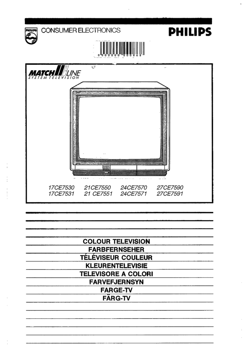
Philips Matchline 21CE7551 operating instructions

Philips

Philips Matchline 21CE7551 operating instructions

Panasonic Genus TX-G10 operating instructions

Panasonic

Panasonic Genus TX-G10 operating instructions

Toshiba 19A20 Service manual

Toshiba

Toshiba 19A20 Service manual

Philips 25PT4523-16 manual

Philips

Philips 25PT4523-16 manual

Sony XBR-100Z9D reference guide

Sony

Sony XBR-100Z9D reference guide

Philips PR0930X3 owner's manual

Philips

Philips PR0930X3 owner's manual

https://manuals.online logo
https://manuals.online logoBrands
  • About & Mission
  • Contact us
  • Privacy Policy
  • Terms and Conditions

Copyright 2026 Manuals.Online. All Rights Reserved.

Service (New zealand )
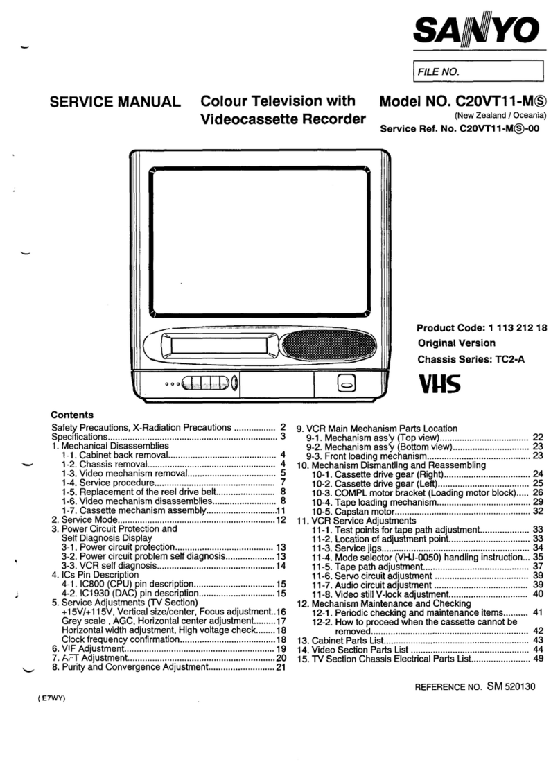
Service Manual Colour Television Ref. No. CZP3359TX-00
Model No. CZP3359TX
4
llhh~l ,,1111 I I
CONTENTS Page
1. SAFETY PRECAUTIONS .............. 1
2. SPECIFICATIONS SUMMARY .......... 2
3. CHASSIS DESCRIPTION ............. 3-4
4. BLOCK DIAGRAM ................... 5
5. DISASSEMBLY ..................... 6
6. CIRCUIT ALIGNMENT ............... 7-9
7. SERVICE CONTROL ADJUSTMENTS ..... 10-13
8. CABINET PARTS LIST .............. 14
9. TUNER CIRCUIT DIAGRAM ........... 15
10. CHASSIS ELECTRICAL PARTS LIST ...16-41
11. CIRCUIT OIAGRAM
ORIGINAL VERSION
Chassis Series E3-633
Give complete “SERVICE REF. NO.” for parts
order or servicing, it is shown on the
rating sheet at cabinet back of the unit.
~ote
This T.V. receiver will not work properly
in aforeign countries where the television
transmission system and poww source differ
form the design specifications. Refer to
the specifications for the design
specif icat ions.
D8EV
\
Reference No.wM-5m53
SAFETY PRECAUTIONS
1. An isolation transformer should be connected
in the power Iine between the receiver and
the AC Iine when aservice is performed on
the pr imar yof the converter transformer of
the set.
2. Compi ywith al itaut ion and saf et y-related
notes provided on the cabinet back, inside
the cabinet, on the chassis or the picture
tube.
3. When replacing achassis in the cabinet,
always be certain that all the protective
devices are installed proper Iy, such as,
control knobs, adjustment covers or
shields, barriers, isolation resistor-
capacitor networks etc.
Before returning any television to the
customer, the service technician must be
sure that it is completely safe to operate
without danger of electrical shock.
X—RAD IAT 10N PRECAUT 10N
The primary source of X-RADIATION in television receiver is the picture tube. The picture tube
is specially constructed to Iimit X-RADIATION emissions. For cent inued X-RADIATION protection,
the replacement tube must be the same type as the original including suffix letter. Excessive
high voltage may produce potent ial Iyhazardous X-RADIATION. TO avoid such hazards, the high
voltage must be maintained within specified limit. Refer to this service manual, high voltage
adjustment for specific high voltage limits. If high voltage exceeds specified limits, take
necessary corrective action. Carefully follow the instructions for +Bl volt power supply
adjustment, and high voltage adjustment to maintain the high voltage within the specified
limits.
PRODUCT SAFETY NOT ICE
—-
Product safety should be considered when acomponent rep Iacement is made in any area of a
receiver. Components indicated by mark ~inthe parts Iist and the schematic diagram designate
components in which safety can be of special significance. It Is particular Iyrecommended that
only parts designated on the parts Iist in this manual be used for component rep Iacement
designated by mark~.No dev iat ions from resistance wattage or voltage ratings may be made for
replacement iterns designated by mark ~,
-l–
SPEC IFI CAT 10NS
iPower source AC 230V, 50Hz
(
~Power consumption 100W CENELEC
~Television system \System -BIG
IColour system IPAL
I
IChannel coverage VHF 1-11
UHF 21-69
WIColour :3447 MHz
iAudio output I15W, 10~ distortion
ISpeaker I05”2,c$1OX4 8ohm
Picture tube
High voltage
Semiconductors
Dimensions
Weight
Ext. terminal
21-pin terminal
Audio monitor out
S-terminal in
Audio in
78 cm diagonal, 110 degree I
Type No, A78JVB61X(RU)
27 KV at Zero beam
149 Transistors
56 ICS I
Width 810 mm
Height 701 mm
Oepth 552 mm
CENELEC standard
RCA type, Rand L
S-VHS VCR standard
RCA type, Rand L
SUMMARY
This TV set al Iowa vou to receive CC IR-BIG system,
Two way speaker system Hi-Fi sound, and more powerful sound can be enjoyed by using audio monitor terminal.
61 function infra-red remote control including the teletext control.
Up to 30 broadcast stations in your reception area can be automat ical Iyfound by the frequency tuning system and
stored in the memory.
CENELEC standard 21-PIN terminals is provided, so aVCR, video disc player or other AV apparatus can be connected.
S-terminal is provided, so the VCR (S-VHS type) is can be connected,
The TELETEXT decoder is built in.
CONTROLS
I.STEREO/BILINGUAL
/---M-#
TV channel and programme
number indicator h,oI&
Power indicato
w
C(L)(D
~:
Main ON/OFF switch
1
PIP Colour &Brightness Control Programme UP/DOWN Programme Search
Contrast
(1
~x ,Tm~ ~]+ ‘A?
oQ,%
/3
Head Phone Volume Memory TV/AVSwilch
speaker is automatically
switched off.
–2–
CHASSIS DESCRIPTION
POWER SUPPLY
The power SUPPI ycircuit of the E3B chassis is composed
of arectifier smoothing circuit, an oscillation
circuit, acontrol circuit and an output rectifier
circuit.
The AC input VOI tage is ful l-wave rectified by the
rectifier smoothing circuit, and an astable DC voltage
is generated at both terminals of tha smoothing
capacitor C320. This voltage is input to the oscillation
circuit. The oscillation circuit is provided with a
blocking oscillator circuit that switches the switching
transistor Q323 ON and OFF, and an osci IIation frequency
and aduty square wave pulse are generated in the input
windings according to the operation of the control
circuit. Asquare-wave pulse whosa size is dependent on
the turn ratio of the input and output windings is
obtained in the output winding. This is rectified in the
output rectifier circuit, and the desired DC voltage is
obtained.
IF &DEFl_ECTION
The IF output signal from the tuner passes through the
SAW filter, and it is input to pin (6) and pin (7) of
IC180 and is input to pin (4) and pin (3) of ICICO.
Tha signal input to the IC180 passes through the IF
amplifier, video detection and video amplifier circuits
and it is output from pin (22) as acomposite video
signal, The output signal from pin (22) also passes
through the 5.5 MHz trap circuit of X197, and it is
input to pin (6) of IC2A0. The signal input to the ICICO
passes through the SIF amplifier, FM detector, volume
control and audio output circuit, and it is then output
from pin (15) as audio drive signal.
The sync. separation circuit separates the video signals
to vertical- and horizontal -sync .signals respect ivel y.
The horizontal-sync. signal passes through the IC401 and
it is applied to the gating circuit, and performs the
horizontal oscillation trigger.
The horizontal oscillation occurs as a result of the
circuit configuration consisting of C415, R420, VR411
and pin (15), and the horizontal free oscillation
frequent yis adjusted from pin (14). VR41O is for
adjustment of the horizontal cantring.
The separated vertical -sync .signal from the sync. -
separation circuit passes through the vertical-
separation circuit, and applied to the trigger divider
circuit. The horizontal oscillation pulse and input
vertical -sync .pulse are monitored by the trigger divider
circuit, and the switching (50Hz /60Hz) system.
The vertical amplitude is adjusted for 50Hz and 60Hz
automatically.
The output signal from the trigger divider is triggered
by the vertical oscillation circuit consisting’ of R404,
C404 and pin (4), and vertical drive pulse output from
VR405 is for changing the amount of AC feedback applied
to pin (2) and for adjustment of the vertical amplitude.
AUDIO OUTPUT <TDA1521>
The audio signal output from pin (13),(15) of IC850 is
input to pin (l),(9) of IC390 and passes through the
preamplifier circuit and the drive circuit, after that
it is input to the audio amplifier. The audio amplifier
is an SEPP (single-ended, push-pull) OTL type and
outputs to pin (4),(6) to drive the speaker directly.
VI DEO, CHROMA &R. G.B.
The composite video signal output from the pin (22) of
IC180 passes through Q1C3, Q5F2 and Q5F5, and it is
supplied to pin (15) of IC270 as the luminance (Y)
signal, to pin (15) of IC200 as the chroma signal.
The luminance signal input to the pin (15) of IC270 is
applied to the luminance amplifier and the contrast
control circuit. The gain control (contrast) is applied
by the pin (19) as DC voltage, and this signal is then -
input to the matrix circuit. The DC level of the
luminance signal can be varied (brightness) by the OC
voltage of pin (20).
The chroma signal input to pin (15) of IC200 passes
through the chroma amplifier, the saturation control,
the contrast control, and the output amplifier circuit,
and it is output to pin (12). The chroma signal output
to pin (11),(12) is input to the lH delay line circuit,
and ie divided into R-Y and B-Y chroma signals, and are
input to pin (11) respectively. The R-Y chroma signal
input to pin (11)isdetected by the CW signal which has
aphasa inversion of 180° every lH at the PAL switching
circuit, and is then taken out to the R-matrix circuit
as R-Y demodulated output. The B-Y chroma signal is
detacted by the CW signal which has no phase inversion,
and is then takan out to B-matrix circuit as B-Y
demodulated output. Tha R-Y and B-Y demodulated output
are matrixed G-Y matrix circuit, and G-Y demodulated
output taken out to G-matrix circuit.
The each R.G. B. matrix circuits are mixed the luminance
signal and aach R-Y, G-Y and B-Y demodulated output ._,
signal to obtain the red, green and blue primary colour
signals, and is applied tha each R.G.B. amplifier
circuits in the IC270. Tha signal passes through the
R.G,B. amplifier circuit are added to the blanking pulsa
which is producted by the sandcast signal input to pin
(10), and output to pin (1) as red signal, to pin
(3) as green signal, to pin (5) as blue signal.
The reference osci IIator operates at twice tha
subcarrier frequency which phase and frequency are
controlled by the burst phase and the fraquency of the
chroma signal. The oscillator can be adjusted by the
voltage of the phase detector output.
–3–
VERT ICAi_ OUTI=%JT
An IC (LA7831) is used for the vertical output circuit
In this chassis. The vertical drive pulse from pin (1)
of IC401 is input to pin (6) of IC450. This pulse drives
IC450, and the vertical scanning is performed. Inthe
first half of scanning adeflecting current is output
from pin (4) and passes through the following path:
VCC25V+ D450+ pin(5)+ pin(4)+ DY+ C451=D VR405.
An electric charge is then stored in C451. In the last
half of scanning the current path is C451+ DY+ pin(4)
+pin(6)+ VR405+ C451. In this way, an amplifying
sawtooth waveform current flows directly to DY to
perform the electron beam deflection.
Next, in the first half of the blanking period the
vertical drive pulse suddenly becomes OFF, and in order
to reduce the current flowing to OY, the current path
becomes to follow by the inductance of DY: DY+
pin(4).+ pin(6)+ VR405+ C451+ DY. Also, when the
charge of OY has dissipated, the current path becomes
VCC25V+ pin(8)+ pin(9)+ C457=D pin(5)+ pin(4)+ DY+
+C451+ VR405 and when the prescribed current value is
reached enough, the vertical drive pulse becomes ON,
This completes one cycle.
Horizontal_ OUTPUT
Ahorizontal oscillation signal is output from pin (11)
of IC401 and switches the drive transistor Q490. This
switching signal current is amplified by the drive
transformer T490 and drives the output transistor Q493.
When Q493 becomes ON, an amplifying current flows
directly to OY through C476+ L475JR479+ DY+ Q493+
+GND, and deflection is performed in the last half of
the scanning period.
Next, when Q493 becomes OFF, the charge that had bean
stored in OY up to that point releases aresonance
current to the resonant capacitors C493 and C494 and
charges them. The current stored in C493 and C494 is
then flowed back to DY, and an opposite charge is then
stored in OY. This opposite charge then switches the
dumper diode In Q494 ON, the resonance state is
completed, and an amplifying current is then flowed
again directly to DY through the dumper diode. By this
means, the deflection in the first half of the scanning
period is performed, and when Q493 becomes ON at
end of the first half of the scanning period,
deflection during the last half is begun,
completing one cycle.
the
the
thus
HIGH VOLTAGE
The 1000VP-P blanking pulse is generated in the primarY
coil of the flyback transformer T480, and it is boosted
10- 15 times, and astable high-voltage pulse superposed
with harmonics nine times, and the fundamental harmonics
IS generated. This is made into a20-30kV DC voltage by
using adouble-voltage rectifier circuit. Furthermore,
the intermediate voltage of the double-voltage rectifier
circuit is divided by the resistance, and used as the
focus and the screen vo Itages for the CRT. This
resistance for the potential division is unified in the
flyback transformer.
Moreover, the accompanying coils are used to generate
the heater voltage, and An pulse.
–4–
TINT
%“ Iw
?5 I
PHASE
c
“’~” 19 II’1’ ’41 18 171 ‘--I-
,9 PIP 1/0
7AV 1/0
o
u
UNIT ==mr o0
00
00
00
0-
01 C3 —
II l-.
%7
,F Q155 SAW
FILTER
AGC
(D/K
o‘1
o
0J
o
00
00
El
UNIT F4ilE&!li
Q1 KO Q1 LO
19 L= v4
I
u-l
I
-11
I1
,5 Q1C8 QIE;
w
SIF —
.FM I
IMAIN UNIT 11I---+c”
IC401
Q490 1
HoRlz
DRIVE I
[1
POWER UNIT E155V
25V
25V
I
—1
n
-$t- Q329
I I I Ill-– –––– –--l
=
12V
IC380
5V
IC381
M
Q320 Q322
ERROR ERROR II ~ 6.5V
DET. DRIVE DEFLECTDN
YCUE +:”” -— —–- -- Jl--
— — —
DISASS EM SLY
L
{
‘\
A— .—
I
I
A
B
I
.
..
L.
I
B
o
‘1”
.
0
~ t
.
●
9
“;I
D
.
Zjll
o
===1
$
0
—- A
CABINET BACK REMOVAL
Remove 16 screws (A).
Then draw off the cabinet back.
J
o
. .
. .
. .
0
PICTURE TUBE RBJOVAL
Caution:
Do not disturb the deflection yoke assembly on
CRT neck. Care must be taken to keep these
assamb Iies intact. Discharge picture tube by
shorting the anode connection to chassis ground.
(Not cabinet or other mounting parts. )
Remove the cabinet back and chassis,
Place the cabinet face down on asoft surface.
Remove 4screws (B).
Gently lift out the picture tube and place it on a
soft surface.
Install replacement picture tube in reverse order.
–6–
\
CIRCUIT Al_ IGNMENT
Fig.1 Input probe
IOkn
Fig.3 Damping R
100 ohm
won
v
[VIF ALIGNMENT ]
Fig.2 (Mmut probe
O.002u F
~?
Fig.4 Input probe (Trap adj.) Fig.5 Short clip
DETECTOR ADJ. TRAP ADJ. OVERALL WAVEFORM
DC 12V TP-4G TP-4G TP-4G
AGC voltage TP-l CTP-l CTP-l C
sOutput probe lC180-6pin a-side Tuner-TP a-side Tuner-TP b-side
EInput probe Q1 C3-E Q1 55-C Fig.3 Q1 C3-E
TShort clip lC180-7pin
TDamping RTP-lD
ISystem SW 6/G(38.9), 1(39.5) B/G B/G or I
NBand VHIGH VHIGH
GSweep ATT 30dB 20dB 18dB
Tuning voltage —lCl10-15pin
By using T185, By using T143. By using the tuner
adjust “P” to the bring the trap to converter coil and
maximum, A(40.4). T137, make the
Adjustment P(38.9/39.5) By using T140. marker positions
bring the trap to to P=38*5% (B/G)
A’(31.9). P=40*5% (1)
=
VIF waveform
A~j-
A“(31.9) (40.4) AA’ SA
–8–
[AFT ALIGNMENT ]
SETTING OF AGC VCENTER FADJ,
DC 12V
A’GC voltage
Output probe
Input probe
Short clip
Damping R
System SW
Band
SG output
s
E
T
T
I
N
G
TP-4G
TP-lC
Tuner-TP b-side
Q1 C3-E
TP-4G
TP-lC
lC180-6pin a-side
TP-lT
IC180-7pin
TP-lD
B/G, IB/G, I
VHIGH
40mVrms
VH IGH
Fix the AGC
voltage for the
waveform to be
1,0 vp_ra,
By using T182,
adjust SG output
to be equal to the
base line,
Adjustment Fig.6
o.oIPF’
+
38.9 (39.51
[Rasc
Lint
Sc Outpst
Pwl Yr
_m
c“’
1Vp-p
c?
c’
VIF waveform Fig,7 O.OIN
A’ SA* 39kn
[SIF ALIGNMENT ]
FM DETECTOR ADJ.1 FM DETECTOR ADJ.3FM DETECTOR ADJ,2
—
s
E
T
T
I
N
G
—
DC 12V
AGC voltage
Output probe
Input probe
V-meter
System SW
carrier
modulation
TP-4G
TP-lJ
lCICO-3pin a-side
lCICO-19pin
TP-4G
TP-1 J
lCICO-17pin Fig.6
TP-lL Fig.7
lCICO-15pin
B/G(5.5MHz)
I(6.OMHZ)
1KHz, sine-wave
TP-4G
TP-lJ
lCICO-6pin Fig.6
TP-lK Fig.7
lCICO-10pin
B/G(5.74MHz)B/G(38,9),l(39.5)
1KHz, sine-wave
By using TIEO,
adjust the DC
voltage of the
lCl10-10pin to
4. Ov.
or adjust “B” to
the maximum,
Adjust AGC voltage
for “A” to be
0.5 via-p.
By using T1E4,
adjust the DC
voltage of the
lCl10-15pin to
4, Ov,
or adjust “A” to
the maximum.
Adjustment By using T1L2,
adjust “P” to be
on the center line
mEl
P(38.9)
(39.51 %BiI
VIF waveform
—
–9–