Seco SECOMX-945/N270 User manual

SECOMX-945/N270
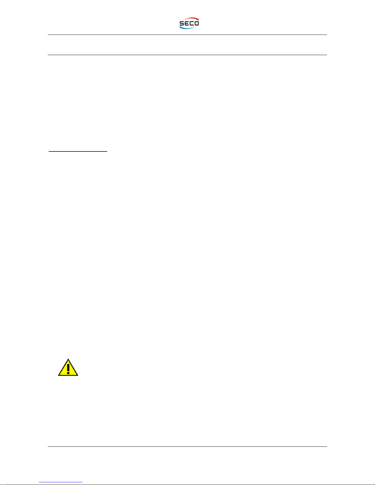
XTX™Module based on Intel®Atom™platform
SECOMX-945/N270
User Manual

SECOMX-945/N270
User Manual - Rev. First Edition: 0.1 - Last Edition: 2.1 - Author: S.B. - Reviewed by G.M.
Copyright © 2011 SECO s.r.l.
SECOMX-945/N270
pag. 2
REVISION HISTORY
Revision
Date
Note
Rif.
0.1
15/06/2009
First release preliminary
SB
1.0
25/06/2010
First official release
SB
1.1
27/12/2010
BIOS Section updated
“I/O mapping – IRQ” chapter added
SB
1.2
14/03/2011
BIOS Section updated
SB
1.3
29/06/2011
BIOS Section updated
SB
2.0
22/07/2011
New release related to board version with Realtek Ethernet controller
SB
2.1
26/09/2011
Technical features updated
Optional signals paragraph updated (par. 3.2.2.5)
IDEx Master and Slave identification added (par. 4.3.16)
Internal IDE/SATA mode paragraph updated (par. 4.4.14)
SB
All rights reserved. All information contained in this manual is confidential material and
property of SECO S.r.l.
Unauthorised use, duplication, modification or disclosure of the information to a third-party by any
means without prior consent of SECO S.r.l. is prohibited.
Every effort has been made to ensure the accuracy of this manual; however, SECO S.r.l. accepts
no responsibility for any inaccuracies, errors or omissions herein. SECO S.r.l. reserves the right to
change specifications without prior notice in order to supply the best product possible.
For more information on this and other SECO products, please visit our web-site at:
http://www.seco.com
related issues or software@seco.com for software related issues, specifying the product model
and describing the current problem.
SECO Srl - Via Calamandrei 91
52100 Arezzo –ITALY
Ph: +39 0575 26979 - Fax: +39 0575 350210
http://www.seco.com

SECOMX-945/N270
User Manual - Rev. First Edition: 0.1 - Last Edition: 2.1 - Author: S.B. - Reviewed by G.M.
Copyright © 2011 SECO s.r.l.
SECOMX-945/N270
pag. 3
INDEX
CHAPTER 1. INTRODUCTION....................................................................................................5
1.1 WARRANTY............................................................................................................................................ 6
1.2 INFORMATION AND ASSISTANCE .............................................................................................................. 7
1.3 RMA NUMBER REQUEST......................................................................................................................... 7
1.4 SAFETY ................................................................................................................................................. 8
1.5 ELECTROSTATIC DISCHARGES................................................................................................................ 8
1.6 ROHS COMPLIANCE ............................................................................................................................... 8
CHAPTER 2. OVERVIEW............................................................................................................9
2.1 INTRODUCTION..................................................................................................................................... 10
2.2 TECHNICAL SPECIFICATIONS................................................................................................................. 11
2.3 ELECTRICAL SPECIFICATIONS................................................................................................................ 12
2.4 MECHANICAL SPECIFICATIONS .............................................................................................................. 12
2.5 HEAT-SPREADER.................................................................................................................................. 13
2.6 BLOCK DIAGRAM .................................................................................................................................. 14
CHAPTER 3. CONNECTORS....................................................................................................15
3.1 CONNECTORS OVERVIEW ..................................................................................................................... 16
3.2 CONNECTORS DESCRIPTION ................................................................................................................. 17
3.2.1 SO-DIMM DDR2 Socket.............................................................................................................. 17
3.2.2 XTX™module connectors............................................................................................................ 17
CHAPTER 4. BIOS SETUP........................................................................................................23
4.1 INTRODUCTION..................................................................................................................................... 24
4.2 BASIC CMOS CONFIGURATION............................................................................................................. 25
4.3 ADVANCED CMOS CONFIGURATION..................................................................................................... 26
4.3.1 Display tests behaviour................................................................................................................ 26
4.3.2 Show Graphic Logo ..................................................................................................................... 26
4.3.3 RAM test execution...................................................................................................................... 26
4.3.4 NumLock State at Boot................................................................................................................ 26
4.3.5 Ignore keyboard error .................................................................................................................. 26
4.3.6 Typematic Programming.............................................................................................................. 26
4.3.7 Typematic Rate Delay ................................................................................................................. 26
4.3.8 Typematic Rate............................................................................................................................ 27
4.3.9 Wait for F1 on error...................................................................................................................... 27
4.3.10 Power Button Instant OFF........................................................................................................... 27
4.3.11 Ignore IDE 80 cable check........................................................................................................... 27
4.3.12 Console redir. port ....................................................................................................................... 27
4.3.13 Console redir. after boot.............................................................................................................. 27
4.3.14 Seek Hard Drive at Boot.............................................................................................................. 27
4.3.15 Sec. to wait for HD reset.............................................................................................................. 27
4.3.16 First / Second / Third / Fourth boot device .................................................................................. 27
4.3.17 Internal video boot on .................................................................................................................. 28
4.3.18 Boot video first from..................................................................................................................... 28
4.3.19 USB Keyboard after boot............................................................................................................. 28
4.3.20 Hyper-Threading.......................................................................................................................... 28
4.3.21 PCI Latency ................................................................................................................................. 28
4.3.22 Console redir. baud rate .............................................................................................................. 28
4.4 CHIPSET CONFIGURATION .................................................................................................................... 29
4.4.1 PCI Slot 1 / 2 / 3 /4....................................................................................................................... 29
4.4.2 PCI Express Slot 1 / 2 / 3 / 4........................................................................................................ 29
4.4.3 Onboard LAN device ................................................................................................................... 29
4.4.4 PCI INTA / other device IRQ........................................................................................................ 29
4.4.5 PCI INTB / SMBUS / USB2-3 IRQ............................................................................................... 29
4.4.6 PCI INTC / USB 4-5 IRQ ............................................................................................................. 29
4.4.7 PCI INTD / USB 6-7 IRQ ............................................................................................................. 29
4.4.8 POST Port 80H decode............................................................................................................... 30

SECOMX-945/N270
User Manual - Rev. First Edition: 0.1 - Last Edition: 2.1 - Author: S.B. - Reviewed by G.M.
Copyright © 2011 SECO s.r.l.
SECOMX-945/N270
pag. 4
4.4.9 Internal SMBUS PCI device......................................................................................................... 30
4.4.10 Internal Audio type....................................................................................................................... 30
4.4.11 Internal UHCI USB ports.............................................................................................................. 30
4.4.12 Internal EHCI USB....................................................................................................................... 30
4.4.13 Maximum UDMA mode................................................................................................................ 30
4.4.14 Internal IDE/SATA mode ............................................................................................................. 30
4.4.15 Thermal Management.................................................................................................................. 30
4.4.16 Maximum CPU frequency MHz ................................................................................................... 30
4.4.17 Chipset Spread Spectrum............................................................................................................ 31
4.4.18 LVDS Spread Spectrum %.......................................................................................................... 31
4.4.19 Internal IGD Memory MB............................................................................................................. 31
4.4.20 Internal IGD function 1................................................................................................................. 31
4.4.21 Internal Flat Panel type................................................................................................................ 31
4.4.22 PEG graphics device ................................................................................................................... 31
4.5 SUPER I/O CMOS CONFIGURATION...................................................................................................... 32
4.5.1 COMA / COMB base address...................................................................................................... 32
4.5.2 COMA / COMB IRQ..................................................................................................................... 32
4.5.3 COMB Interface........................................................................................................................... 32
4.5.4 COMB IrDA signal pin.................................................................................................................. 33
4.5.5 LPT mode .................................................................................................................................... 33
4.5.6 LPT IRQ....................................................................................................................................... 33
4.5.7 FDC Controller............................................................................................................................. 33
4.5.8 Parallel connected to ................................................................................................................... 33
4.5.9 Pointing device (Mouse) .............................................................................................................. 33
4.6 POWER MANAGEMENT ......................................................................................................................... 34
4.6.1 Power Failure Resume Type....................................................................................................... 34
4.6.2 Speed Step support..................................................................................................................... 34
4.6.3 ACPI tables.................................................................................................................................. 34
4.6.4 C-State support............................................................................................................................ 34
4.6.5 Enhanced C-State support .......................................................................................................... 35
4.6.6 Maximum C-State allowed........................................................................................................... 35
4.6.7 T-State support............................................................................................................................ 35
4.6.8 ACPI S4/S5 Shutdown................................................................................................................. 35
4.7 I/O MAPPING -IRQ ........................................................................................................................... 36
4.7.1ISA Addressing............................................................................................................................ 36
4.7.2 IRQ Mapping................................................................................................................................ 37
4.7.3 ISA IRQ mapping considerations................................................................................................. 37
4.7.4 Floppy Disk Controller Enabling .................................................................................................. 38

SECOMX-945/N270
User Manual - Rev. First Edition: 0.1 - Last Edition: 2.1 - Author: S.B. - Reviewed by G.M.
Copyright © 2011 SECO s.r.l.
SECOMX-945/N270
pag. 5
Chapter 1.INTRODUCTION
Warranty
Information and assistance
RMA number request
Safety
Electrostatic Discharges
RoHS compliance
SECOMX-945/N270
User Manual - Rev. First Edition: 0.1 - Last Edition: 2.1 - Author: S.B. - Reviewed by G.M.
Copyright © 2011 SECO s.r.l.
SECOMX-945/N270
pag. 6
1.1 Warranty
This product is subject to Italian law D. Lgs 24/2002, acting European Directive 1999/44/CE on
arguments of sale and warranties to consumer.
The warranty for this product lasts 1 year
Under the warranty period the Supplier guarantees the buyer an assistance service for repairing,
replacing or credit of the item, at its own discretion.
Shipping costs regarding non-conforming items or items that need replacement, are to be paid by
the customer.
Items cannot be returned unless formerly authorised by the supplier.
The authorisation is released after compiling the specific form available from the web-site
http://www.seco.com (RMA Online). Authorisation number for returning the item must be put both
on the packaging and on the documents brought with the items, which have to be not damaged,
not tampered, with all accessories in their original packaging.
Error analysis form identifying the fault type has to be compiled by the customer and has to be sent
in the packaging of the returned item.
If some of the above mentioned requirements for returning the item is not satisfied, item will be
shipped back and customer will have to pay for shipping costs.
The supplier, after a technical analysis, will verify if all the requirements for warranty service are
met. If warranty cannot be applied, he calculates the minimum cost of this initial analysis on the
item and the repairing costs. Costs for replaced components will be calculated aside.
Warning! All changes or modifications to the equipment not clearly approved by
SECO S.r.l. could impair equipment’s functionality and lead to the
expire of the warranty

SECOMX-945/N270
User Manual - Rev. First Edition: 0.1 - Last Edition: 2.1 - Author: S.B. - Reviewed by G.M.
Copyright © 2011 SECO s.r.l.
SECOMX-945/N270
pag. 7
1.2 Information and assistance
What do I have to do if the product is faulty?
SECO S.r.l. offers the following services:
SECO website: visit http://www.seco.com to receive the last information on the product. In
most of the cases you can find useful information to resolve your problem.
SECO reseller: the reseller or agent can help you in determining the exact cause of the
problem and search the best solution for it.
SECO Help-Desk: contact SECO Technical Assistance.
A technician is at your disposal to understand the exact origin of the problem and suggest the right
solution. E-mail: technical.service@seco.com
Fax (+39) 0575 340434
Repairing centre: it is possible to send the faulty product to SECO Repairing Centre. In this
case, follow this procedure:
Returned items have to be provided with RMA Number. Items sent without RMA
number will be not accepted.
Returned items have to be packed in the appropriate manner. SECO is not responsible
for damages caused by accidental drop, improper usage, or customer neglects.
Note: We ask to prepare the following information before asking for technical assistance:
- Name and serial number of the product;
- Description of Customer’s peripheral connections;
- Description of Customer’s software (operative system, version, application software, etc.);
- A complete description of the problem;
- The exact words of every kind of error message received
1.3 RMA number request
To request a RMA number, please, visit SECO’s web-site. In the home-page select “RMA Online”
and follow the described procedure
You will receive an RMA Number within 1 working day (only for on-line RMA request).

SECOMX-945/N270
User Manual - Rev. First Edition: 0.1 - Last Edition: 2.1 - Author: S.B. - Reviewed by G.M.
Copyright © 2011 SECO s.r.l.
SECOMX-945/N270
pag. 8
1.4 Safety
SECOMX-945/N270 module uses only extremely-low voltages.
While handling the board, it is necessary to be careful in order to avoid any kind of risk or damages
to electronic components. Always switch the power off, and unplug the power supply unit, before
handling the board and/or connecting cables or other boards.
Don’t use metallic components, like paper clips, screws and similar, near the board, when this is
supplied, to avoid short circuits due to unwanted contacts with other components of the board.
Never connect the board to an external power supply unit or battery, if the board has become wet.
Make sure that all cables are correctly connected and are not damaged.
1.5 Electrostatic Discharges
SECOMX-945/N270, like any other electronic product, is an electrostatic sensitive device and
some components on-board could be damaged by high voltages caused by static electricity.
So whenever handling a SECOMX-945/N270 board, take care to ground yourself through an anti-
static wrist strap. Placement of the board on an anti-static surface is also highly recommended.
1.6 RoHS compliance
SECOMX-945/N270 board is designed using RoHS compliant components and is manufactured on
a lead-free production line. It is therefore fully RoHS compliant.
SECOMX-945/N270
User Manual - Rev. First Edition: 0.1 - Last Edition: 2.1 - Author: S.B. - Reviewed by G.M.
Copyright © 2011 SECO s.r.l.
SECOMX-945/N270
pag. 9
Chapter 2.OVERVIEW
Introduction
Technical Specifications
Electrical specifications
Mechanical specifications
Heat-spreader
Block diagram

SECOMX-945/N270
User Manual - Rev. First Edition: 0.1 - Last Edition: 2.1 - Author: S.B. - Reviewed by G.M.
Copyright © 2011 SECO s.r.l.
SECOMX-945/N270
pag. 10
2.1 Introduction
SECOMX-945/N270 is a CPU module, in XTX™format, based on Intel®Atom™CPU interfaced to
Intel®945GME Chipset, that provide most of its standard functionalities.
CPU used on SECOMX-945/N270 module is Intel®Atom™N270 at 1.6 GHz, with 512KB L2
Cache, 533 MHz FSB and Hyper Threading (HT) capabilities. TDP (Thermal Dissipation Power) is
2.5 W.
Intel®945GME chipset provides the access to memory, which is available as a single SODIMM
DDR2 memory module, with a capacity up to 2GB. SODIMM memory modules supported can have
frequencies of 533 or 667MHz.
It also integrates Intel® Graphics Media Accelerator 950, that offers an advanced 2D and 3D
graphic engine, and can pilot directly Flat Panels through LVDS interface, standard CRT with RGB
interface, and TV using S-Video or Composite signals.
Many other features come through Southbridge Intel®NH82801GHM (ICH7-M DH), that provides 6
USB 2.0 ports, AC’97 or HD audio interface, PCI Bus, up to four PCI Express x1 ports, one IDE
Channel, two S-ATA channels, LAN interface and LPC bus.
Using these interfaces, there are also other controllers on board, that complete the features of
SECOMX-945/N270 board with two RS-232 ports (at TTL level), one parallel port (optionally
configurable as a Floppy Disk port), PS/2 port for mouse and keyboard, a secondary IDE channel,
Real Time Clock and Watch Dog Timer.
Six mounting holes on the board provide secure mounting to allow the module increased shock
and vibration resistance.
Please refer to following chapter for a complete list of all peripherals integrated and characteristics.
As described in XTX™specifications, all interfacing signals (except SO-DIMM memory socket, that
is directly on XTX™module), are carried out on four 100-pin low profile standard connectors.
Therefore, for external interfacing to standard devices, a carrier board is needed. This board will
implement all the routing of the interface signals to external standard connectors, as well as
integration of other peripherals/devices not already included in SECOMX-945/N270 CPU module.
The carrier board can be designed exactly as needed, both in mechanical dimensions and in
connectors / interfaces desired, and allows the maximum flexibility possible, since the CPU module
can be changed at any moment without lack of compatibility or needing of a new design of the
carrier board.

SECOMX-945/N270
User Manual - Rev. First Edition: 0.1 - Last Edition: 2.1 - Author: S.B. - Reviewed by G.M.
Copyright © 2011 SECO s.r.l.
SECOMX-945/N270
pag. 11
2.2 Technical Specifications
CPU: Intel®Atom™N270 1,6GHz, 512KB L2 Cache, TDP 2.5W
Chipset: Intel® 82945GME + Intel®82801GHM (ICH7M-DH)
Memory: Up to 2GB of 533/667 MHz DDR2 on SO-DIMM socket
FSB: 533 MHz
Graphics: Intel®Graphics Media Accelerator 950
Resolutions: Up to 2048x1536 Q XGA 75 Hz
Dual display supported
LVDS 18 or 24 bit, single or dual channel interface
USB: 6x USB 2.0 ports.
Expansion bus: PCI bus, 4 x PCI Express x1 ports, LPC Bus
ETHERNET: 10/100Mbps Ethernet port, Realtek RTL8103E
PATA: Up to 2 x Ultra ATA/100/66/33 Port
SATA: Up to 2x S-ATA ports
Serial Ports: 2x (TTL level signals)
Parallel Port: 1x (optionally, shared with Floppy Disk Drive Port)
Audio: AC'97 Internal Audio Codec VIA VT1613, external audio interface
PS/2 Keyboard and mouse
Watch Dog Timer
Real Time Clock
Temperature, Fan Speed and Voltage Monitoring
Environmental:
-Power supply +5VDC (+5VSB needed for ATX mode)
-Power consumption: TBD
-Operating Temperature: -20°C ÷ +70°C (*)
Dimensions: 114x95 mm (4.5” x 3.7”)
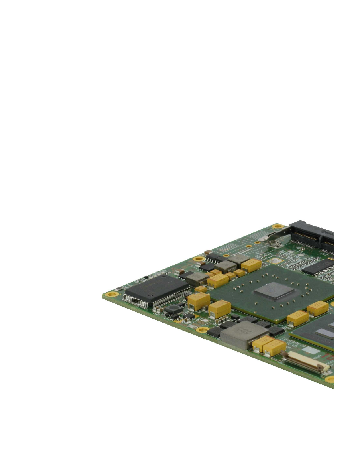
(*) Operating temperature is the temperature reached on any spot of the heat-spreader plate.
It must maintain temperature on the heat-spreader according to the range specified.
According to XTX™specifications, “The heatspreader offered for XTX™modules acts as a thermal
coupling device and is not a heat sink. Heat dissipation devices such as a heat sink with fan or
heat pipe may need to be connected to the heatspreader.”

SECOMX-945/N270
User Manual - Rev. First Edition: 0.1 - Last Edition: 2.1 - Author: S.B. - Reviewed by G.M.
Copyright © 2011 SECO s.r.l.
SECOMX-945/N270
pag. 12
2.3 Electrical specifications
SECOMX-945/N270 board needs to be supplied only with an external +5VDC power supply. +5VSB
Voltage is also needed for working in ATX mode. For real Time Clock working and CMOS memory
data retention, it is also needed a backup battery voltage. All these voltages are supplied directly
through XTX™Connectors X1 ÷ X4.
All remaining voltages needed for board’s working are generated internally from +5VDC power rail.
2.4 Mechanical specifications
According to XTX™specifications, board dimensions are: 114 x 95 mm (4.488” x 3.740”).
Printed circuit of the board is made of ten layers; some of them are ground planes, for disturbance
rejection.
SECOMX-945/N270
User Manual - Rev. First Edition: 0.1 - Last Edition: 2.1 - Author: S.B. - Reviewed by G.M.
Copyright © 2011 SECO s.r.l.
SECOMX-945/N270
pag. 13
2.5 Heat-spreader
SECOMX-945/N270
User Manual - Rev. First Edition: 0.1 - Last Edition: 2.1 - Author: S.B. - Reviewed by G.M.
Copyright © 2011 SECO s.r.l.
SECOMX-945/N270
pag. 14
2.6 Block diagram
CPU
Intel®
ATOM™
Intel®
945GME
Northbridge
Intel® Graphics
Media Accelerator
950
XTX™CONNECTOR
X3
DDR2
System
Memory
FSB
533 MHz
FSB
533/667 MHz
Realtek
RTL8103E
Fast
Ethernet
Controller
Audio
Codec
VIA
VT1613
LPC bus
Intel®
82801GHM
(ICH7-M DH)
Southbridge
LVDS
XTX™CONNECTOR
X4
XTX™CONNECTOR
X1
XTX™CONNECTOR
X2
USB 0 ÷ 3
AC ’97 AUDIO
DMI
Audio
USB ports
PCI
SATA to
PATA Bridge
SIL3811
(optional)
Winbond
Super I/O
W83627
Internal
Firmware
Hub
TV
CRT
SERIAL PORTS
LPT / FLOPPY
Primary IDE Channel
Secondary IDE
Channel
S-ATA 0
S-ATA 2
LAN Interface
ETHERNET
interface
PS/2 MS
+ KEYB
USB 4 ÷ 5
S-ATA 2 (Optional)
SPI
4x PCI Express x1
LPC bus
WatchDog
FAN
Power management

SECOMX-945/N270
User Manual - Rev. First Edition: 0.1 - Last Edition: 2.1 - Author: S.B. - Reviewed by G.M.
Copyright © 2011 SECO s.r.l.
SECOMX-945/N270
pag. 15
Chapter 3.CONNECTORS
Connectors overview
Connectors description

SECOMX-945/N270
User Manual - Rev. First Edition: 0.1 - Last Edition: 2.1 - Author: S.B. - Reviewed by G.M.
Copyright © 2011 SECO s.r.l.
SECOMX-945/N270
pag. 16
XTX™
Connector
X1
XTX™
Connector
X2 (X7)
XTX™
Connector
X3
XTX™
Connector
X4
SO-DIMM
DDR2 Socket
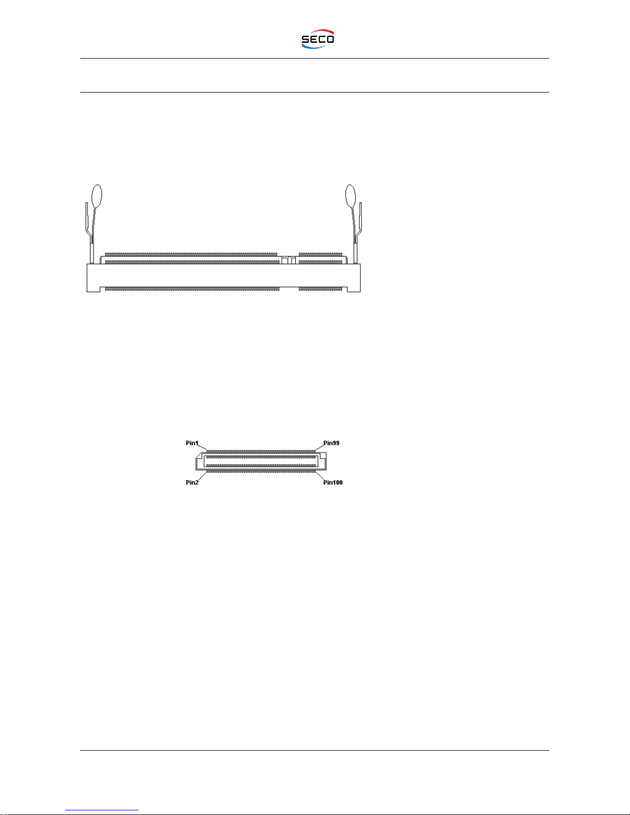
3.1 Connectors overview
According to XTX™specifications, all interfaces to the board are available through the four 100 pin
connectors X1 ÷ X4.
Top side
Bottom side
SECOMX-945/N270
User Manual - Rev. First Edition: 0.1 - Last Edition: 2.1 - Author: S.B. - Reviewed by G.M.
Copyright © 2011 SECO s.r.l.
SECOMX-945/N270
pag. 17
3.2 Connectors description
3.2.1 SO-DIMM DDR2 Socket
Intel® 82945GME Northbridge provides support to 533/667MHz DDR2 memories.
For use of this memories, on board there is a SO-DIMM DDR2 socket, type Tyco 1473006-4 or
equivalent, a right angle, low profile, reverse type socket, used for high speed system memory
applications.
3.2.2 XTX™module connectors
For the connection of XTX™CPU modules, on board there are 4 connectors, type HIROSE FX8-
100S-SV (100 pin, ultra slim, 0.6mm pitch, h=2.25mm), as requested by XTX™specifications.
The pinout of these connectors will be briefly described in the following paragraphs. Please refer to
XTX™standard for a better description of each signal.
Some signals are optional, depending on SECOMX-945/N270 module configuration. See the
description at the end of this document for the list of signals that are not always present (they are
also highlighted in light blue in the following tables, however).

SECOMX-945/N270
User Manual - Rev. First Edition: 0.1 - Last Edition: 2.1 - Author: S.B. - Reviewed by G.M.
Copyright © 2011 SECO s.r.l.
SECOMX-945/N270
pag. 18
3.2.2.1 X1 CONNECTOR: PCI Bus, USB, Audio
Pin
Signal
Pin
Signal
Pin
Signal
Pin
Signal
1
GND
2
GND
51
+5VDC
52
+5VDC
3
PCICLK3
4
PCICLK4
53
PCI_PAR
54
PCI_SERR#
5
GND
6
GND
55
PCI_PERR#
56
RESERVED
7
PCICLK1
8
PCICLK2
57
PCI_PME#
58
USB_D2-
9
PCI_REQ3#
10
PCI_GNT3#
59
PCI_LOCK#
60
PCI_DEVSEL#
11
PCI_GNT2#
12
+3.3VDC
61
PCI_TRDY#
62
USB_D3-
13
PCI_REQ2#
14
PCI_GNT1#
63
PCI_IRDY#
64
PCI_STOP#
15
PCI_REQ1#
16
+3.3VDC
65
PCI_FRAME#
66
USB_D2+
17
PCI_GNT0#
18
RESERVED
67
GND
68
GND
19
+5VDC
20
+5VDC
69
PCI_AD16
70
PCI_C/BE2#
21
PCI_SERIRQ
22
PCI_REQ0#
71
PCI_AD17
72
USB_D3+
23
PCI_AD0
24
+3.3VDC
73
PCI_AD19
74
PCI_AD18
25
PCI_AD1
26
PCI_AD2
75
PCI_AD20
76
USB_D0-
27
PCI_AD4
28
PCI_AD3
77
PCI_AD22
78
PCI_AD21
29
PCI_AD6
30
PCI_AD5
79
PCI_AD23
80
USB_D1-
31
PCI_C/BE0#
32
PCI_AD7
81
PCI_AD24
82
PCI_C/BE3#
33
PCI_AD8
34
PCI_AD9
83
+5VDC
84
+5VDC
35
GND
36
GND
85
PCI_AD25
86
PCI_AD26
37
PCI_AD10
38
AUX_L
87
PCI_AD28
88
USB_D0+
39
PCI_AD11
40
MIC
89
PCI_AD27
90
PCI_AD29
41
PCI_AD12
42
AUX_R
91
PCI_AD30
92
USB_D1+
43
PCI_AD13
44
+5VDC
93
PCI_RST#
94
PCI_AD31
45
PCI_AD14
46
LINEOUT_L
95
PCI_INTC#
96
PCI_INTD#
47
PCI_AD15
48
GND_AUDIO
97
PCI_INTA#
98
PCI_INTB#
49
PCI_C/BE1#
50
LINEOUT_R
99
GND
100
GND
SECOMX-945/N270
User Manual - Rev. First Edition: 0.1 - Last Edition: 2.1 - Author: S.B. - Reviewed by G.M.
Copyright © 2011 SECO s.r.l.
SECOMX-945/N270
pag. 19
3.2.2.2 X2 CONNECTOR: LPC Bus, SATA, PCI Express, ExpressCard, Audio Codec,
additional USB
Pin
Signal
Pin
Signal
Pin
Signal
Pin
Signal
1
GND
2
GND
51
+5VDC
52
+5VDC
3
PCIE_CLK_REF+
4
SATA0_Rx+
53
PCIE1_RX-
54
Not Connected
5
PCIE_CLK_REF-
6
SATA0_Rx-
55
PCIE1_RX+
56
Not Connected
7
GND
8
GND
57
GND
58
IL_SATA#
9
PCIE3_TX+
10
SATA0_Tx-
59
PCIE1_TX-
60
Not Connected
11
PCIE3_TX-
12
SATA0_Tx+
61
PCIE1_TX+
62
Not Connected
13
GND
14
+5VSB
63
PCIE_WAKE#
64
Not Connected
15
PCIE3_RX+
16
SATA1_Rx+
65
SUS_S3#
66
Not Connected
17
PCIE3_RX-
18
SATA1_Rx-
67
GND
68
GND
19
+5VDC
20
+5VSB
69
PCIE0_RX-
70
Not Connected
21
Not Connected
22
SATA1_Tx-
71
PCIE0_RX+
72
Not Connected
23
Not Connected
24
SATA1_Tx+
73
GND
74
Not Connected
25
USB_D5+
26
GND
75
PCIE0_TX-
76
Not Connected
27
USB_D5-
28
+5VDC
77
PCIE0_TX+
78
Not Connected
29
GND
30
Not Connected
79
CODECSET
80
+5VDC
31
PCIE2_TX+
32
SUS_STAT#
81
AC_RST#
82
AC_SDOUT
33
PCIE2_TX-
34
PCI_CLKRUN#
83
+5VDC
84
+5VDC
35
GND
36
GND
85
AC_SYNC
86
AC_SDIN0
37
PCIE2_RX+
38
Not Connected
87
AC_SDIN1
88
AC_SDIN2
39
PCIE2_RX-
40
Not Connected
89
AC_BITCLK
90
FAN_TACHOIN
41
EXC0_CPPE#
42
GND
91
LPC_AD0
92
FAN_PWMOUT
43
Not Connected
44
Not Connected
93
LPC_AD1
94
LPC_FRAME#
45
USB_D4+
46
Not Connected
95
LPC_AD2
96
LPC_DRQ0#
47
USB_D4-
48
WDTRIG
97
LPC_AD3
98
LPC_DRQ1#
49
SUS_S3#
50
SATALED#
99
GND
100
GND

SECOMX-945/N270
User Manual - Rev. First Edition: 0.1 - Last Edition: 2.1 - Author: S.B. - Reviewed by G.M.
Copyright © 2011 SECO s.r.l.
SECOMX-945/N270
pag. 20
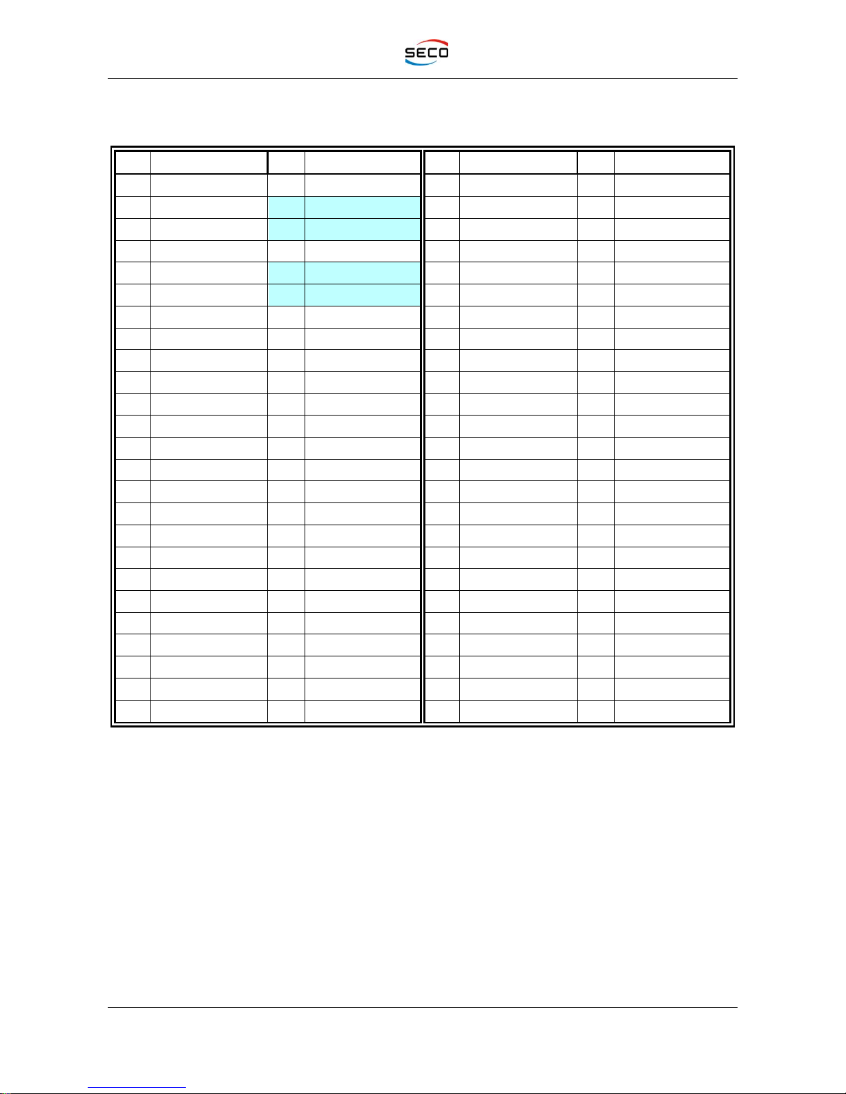
3.2.2.3 X3 CONNECTOR : CRT, LVDS, TV OUT, COM1, COM2, IR, LPT/Floppy, PS/2 Mouse
and Keyboard
Pin
Signal
Pin
Signal
Pin
Signal
Pin
Signal
1
GND
2
GND
51
LPT/FLPY#
52
Not Connected
3
CRT_RED
4
CRT_BLUE
53
+5VDC
54
GND
5
CRT_HSYNC
6
CRT_GREEN
55
STROBE# / N.C.
56
Autofeed# /
Density_Select#
7
CRT_VSYNC
8
CRT_DDC_CLOCK
57
Not Connected
58
PD7 / N.C.
9
Not Connected
10
CRT_DDC DATA
59
IR_RX
60
Error# /
Head_Select#
11
LVDS_CLK_B-
12
LVDS_B3-
61
IR_TX
62
PD6 / N.C.
13
LVDS_CLK_B+
14
LVDS_B3+
63
COM2_RX
64
Init# / DIR#
15
GND
16
GND
65
GND
66
GND
17
LVDS_B1+
18
LVDS_B2+
67
COM2_RTS
68
PD5 / N.C.
19
LVDS_B1-
20
LVDS_B2-
69
COM2_DTR
70
Select_Input# /
Step#
21
GND
22
GND
71
COM2_DCD
72
PD4 / Disk_Change#
23
LVDS_A3-
24
LVDS_B0+
73
COM2_DSR
74
PD3 / Read_Data#
25
LVDS_A3+
26
LVDS_B0-
75
COM2_CTS
76
PD2 /
Write_Protected#
27
GND
28
GND
77
COM2_TXD
78
PD1 /Track0#
29
LVDS_A2-
30
LVDS_CLK_A+
79
COM2_RI
80
PD0 / Index#
31
LVDS_A2+
32
LVDS_CLK_A-
81
+5VDC
82
+5VDC
33
GND
34
GND
83
COM1_RX
84
Acknowledge# /
Drive_Select_1#
35
LVDS_A0+
36
LVDS_A1+
85
COM1_RTS
86
Busy/Wait# /
Motor1#
37
LVDS_A0-
38
LVDS_A1-
87
COM1_DTR
88
Paper End /
Write_Data#
39
+5VDC
40
+5VDC
89
COM1_DCD
90
Select / Write_Gate#
41
LCD_DDC_DATA
42
CASEOPEN#
91
COM1_DSR
92
MS_CLOCK
43
LCD_DDC_CLOCK
44
LCD_BACKLIGHT_
ENABLE#
93
COM1_CTS
94
MS_DATA
45
Not Connected
46
LCD_POWER_ENA
BLE
95
COM1_TXD
96
KEYB_CLOCK
47
TV_DACA_OUT
48
TV_DACB_OUT
97
COM1_RI
98
KEYB_DATA
49
Not Connected
50
TV_DACC_OUT
99
GND
100
GND
Note: signals above highlighted in light blue are shared between Parallel Port and Floppy Drive
Controller. Depending on BIOS settings, they can assume the first or the second meaning,
respectively for parallel port and for Floppy Disk interface. Depending on the type of Super I/O
controller mounted on the board, however, all signals related to Floppy Disk could be totally
absent. In that case, only signals for Parallel port will be present, and there will be no possibility to
enable internal Floppy Disk controller (see also par. 3.2.2.5, 4.2, 4.5.5 and 4.5.7).
Table of contents
Other Seco Motherboard manuals


Popular Motherboard manuals by other brands


Freescale Semiconductor
Freescale Semiconductor MPC8313E PowerQUICC II Pro user guide

NXP Semiconductors
NXP Semiconductors FRDM-KW38 quick start guide

Asus
Asus Z10PE-D16 WS user manual

Asus
Asus A88XM-PLUS manual

THORLABS
THORLABS ELL17 operating manual

Texas Instruments
Texas Instruments Jacinto7 user guide