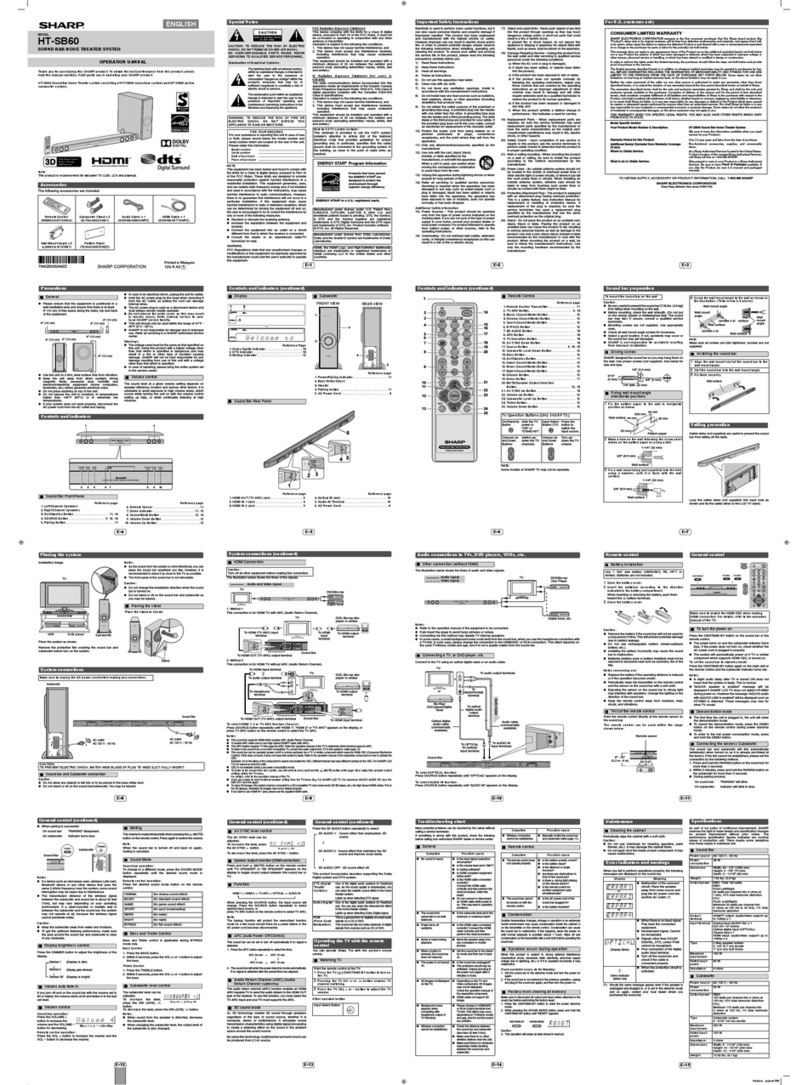
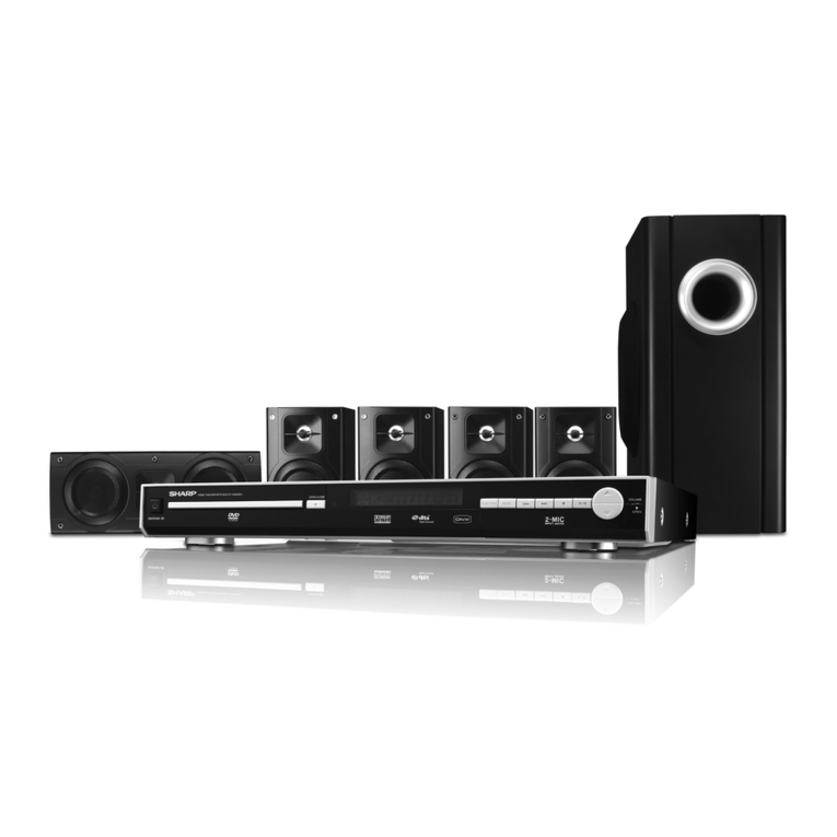
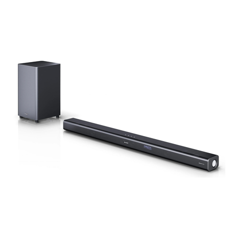
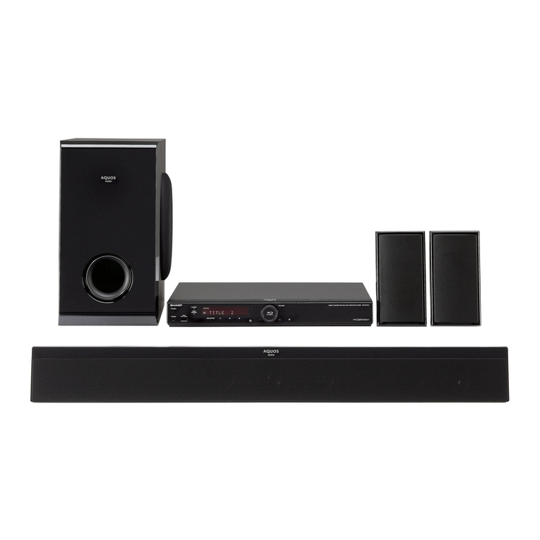
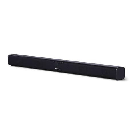
Sharp HT-SB60 User manual

HT-SB60
– 1
This document has been published to be used for
after sales service only.
The contents are subject to change without notice.
BASSTREBLE
AUDIO
3D
PRECAUTIONS FOR USING LEAD-FREE SOLDER
CHAPTER 1. GENERAL DESCRIPTION
[1] Safety Precaution For Service Manual .............. 1-1
[2] Important Service Notes (for U.K. only) ....... 1-1
[3] Specifications .................................................... 1-1
[4] Name Of Parts ................................................... 1-2
CHAPTER 2. ADJUSTMENTS
[1] Test Mode .................................................... 2-1
[2] Abnormal detection distinction at DEMO
Indicator (LED Red) ..................................... 2-2
[3] Manual pairing between the Amplifier and
Subwoofer.................................................... 2-3
CHAPTER 3. MECHANICAL DESCRIPTION
[1] Disassembly ................................................ 3-1
CHAPTER 4. CIRCUIT DESCRIPTION
[1] Waveform Of Wireless Transmission ........... 4-1
[2] Voltage......................................................... 4-2
CHAPTER 5. FLOWCHART
[1] Troubleshooting ........................................... 5-1
CHAPTER 6. MAJOR PART DRAWING
[1] Function Table of IC..................................... 6-1
[2] FL Display .................................................. 6-10
CHAPTER 7. DIAGRAMS
[1] Main (TX) & Subwoofer (RX)
Block Diagram.............................................. 7-1
CHAPTER 8. CIRCUIT SCHEMATICS AND PARTS
LAYOUT
[1] Notes On Schematic Diagram ..................... 8-1
[2] Type Of Transistor And LED ........................ 8-1
[3] Schematic Diagram ..................................... 8-2
[4] Chart Of Connecting Wires.......................... 8-8
[5] Wiring Side Of PWB .................................... 8-9
PARTS GUIDE
SERVICE MANUAL
No. S8232HTSB60HE
CONTENTS
SOUND BAR HOME
THEATER SYSTEM
MODEL
HT-SB60
SHARP CORPORATION
Parts marked with " " are important for maintaining the safety of the set. Be sure to replace these parts with
specified ones for maintaining the safety and performance of the set.
!
• In the interests of user-safety the set should be restored to its
original condition and only parts identical to those specified be
used.
HT-SB60 Sound Bar Home Theater system consisting of
HT-SB60 (sound bar system) and CP-SW60 (active
subwoofer system).
[For Europe, U.K.]

HT-SB60
– 2
PRECAUTIONSFOR USING LEAD-FREE SOLDER
1. Employinglead-free solder
Example:
Indicateslead-free solder of tin, silver and copper.
Lead-free wire solder for servicing
2. Usinglead-free wire solder
When fixing the PWB soldered with the lead-free solder, apply lead-free wire solder. Repairing with conventional
lead wire solder may cause damage or accident due to cracks.
Asthe melting point of lead-free solder (Sn-Ag-Cu) ishigher than the lead wire solder by 40°C, we recommend
youto use adedicated soldering bit, if youare not familiar with how to obtain lead-free wire solder or soldering
bit, contact our service station or service branch in your area.
3.Soldering
Asthe melting point of lead-free solder (Sn-Ag-Cu) isabout 220°C which ishigher than the conventional lead
solder by 40°C, and as it has poor solder wet ability, youmay be apt to keep the soldering bit in contact with the
PWB for extended period of time. However, since the land may be peeled of for the maximum heat-resistance
temperature of partsmay be exceeded, remove the bit from the PWB as soon as youconfirm the steady
soldering condition.
Lead-free solder containsmore tin, and the end of the soldering bit may be easily corrected. Make sure to turn
on and off the power of the bit as required. If adifferent type of solder stayson the tip of the soldering bit, it is
alloyed with lead-free solder. Clean the bit after every use of it.
When the tip of the soldering bit isblackened during use, file it with steel wool or fine sand paper.
Be careful when replacing partswith polarity indication on the PWB silk.
"MAIN/AMPLIFIER, DISPLAY, SUBWOOFER, REGULATOR, SMPS(AMPLIFIER), SMPS(SUBWOOFER),
HDMI, TRANSMIT, RECEIVE PWB" of thismodel employslead-free solder. The LF symbol indicateslead-free
solder, and isattached on the PWB and service manuals.
The alphabetical character following LF showsthe type of lead-free solder.
DescriptionPartsNo.Ref. No.
PWB-A 92LPWB8696MANSMAIN/AMPLIFIER (A1), DISPLAY (A2), SUBWOOFER (A3), REGULATOR (A4)
PWB-B RUiTZA069AWZZ SMPS(AMPLIFIER)
PWB-C RUiTZA070AWZZ SMPS(SUBWOOFER)
PWB-D 92LPWB8695HDMSHDMI
PWB-E RUiTZA082AWZZ TRANSMIT
PWB-F RUiTZA078AWZZ RECEIVE
i

HT-SB60
1 – 3
CHAPTER 1. GENERAL DESCRIPTION
[3]Specifications
WARNING
Thisunit containsno user serviceable parts. Never remove coversunless qualified to do so.
Thisunit containsdangerous voltages, alwaysremove mainsplug from the socket before any service
operation and when not in use for along period.
Sound Bar Subwoofer
[2] Important Service Notes(for U.K. only)
[1] Safety Precaution For Service Manual
Before returning the unit to the customer after completion of arepair or adjustment it isnecessary for the following withstand voltage test to be
applied to ensure the unit issafe for the customer to use.
Setting of Withstanding Voltage Tester and set.
Set name set value
Withstanding Voltage Tester
Te st voltage 4,240 VPEAK
3,000 VRMS
Set time 6 secs
Set current (Cutoff current) 4 mA
Unit
Judgment
OK: The “GOOD” lamp lights.
NG: The “NG” lamp lightsand the buzzer sounds.
PROBE
AC
OUT
UNIT
SHORT-CIRCUIT
AC POWER
SUPPLY CORD
CONNECT THE PROBE
TO SHELL OF AUDIO LINE IN
WITHSTANDING
VOLTAGE TESTER
Power source AC 220 - 240 V ~ 50/60 Hz
Power
consumption
Power on: 38 W
Power standby: 0.4 W (*)
Dimension
Output
terminal
HDMI™ (audio/video support up to
1080p) x 1
Input
terminal
Power source AC 220 - 240 V ~ 50/60 Hz
Power
consumption
33 W
Output power RMS: 150 W (10% T.H.D.)
RMS: 120 W (1% T.H.D.)
Type Subwoofer system
16 cm (6 - 5/16") woofer
Maximum
input power
300 W
150 W
Width: 1385 mm (54 - 1/2")
Height: 73mm (2 - 7/8")
Depth: 68mm (2 - 11/16")
Weight 3.6 kg (7.92 lbs.)
Output power
analogue input (AUDIO IN): x 1
500 mV / 47 kohms
Optical digital input (OPTICAL):
Square type x 1
HDMI input: (audio/video support up to
1080p) x 2
Type 2 Way speaker system
5.7 cm (2 -1/4") woofer
2.5 cm (1") Soft Dome
160 W
Maximum
input power
Rated input
power 80 W
Impedance 4 ohms
(*) Thispower consumption value isobtained when the
sound bar isin low power consumption mode. (Demo
indicator turnsoff).
DimensionsWidth: 144 mm (5 - 11/16")
Height: 430 mm (16 - 15/16")
Depth: 306 mm (12 - 1/16")
Weight 6.1 kg (13.42 lbs.)
RMS: Total 160 watts
RMS: 160 W (80 W + 80 W) (10% T.H.D.)
RMS: 120 W (60 W + 60 W) (1% T.H.D.)
Rated input
power
3ohms
Impedance
1 – 1

HT-SB60
1 – 4
[4] NamesOf Parts
1. Left Channel Speakers
2. Right Channel Speakers
3. On/Stand-by Button
4. SOURCE Button
5. PairingButton
6. Remote Sensor
7. Demo Indicator
8. Sound Mode Button
9. Volume Down Button
10. Volume Up Button
Sound Bar Front Panel
1. Dolby Digital Indicator
2. DTSIndicator
3. MutingIndicator
Display
1. HDMI OUT (TV ARC) Socket
2. HDMI IN 1 Socket
3. HDMI IN 2 Socket
4. Optical IN Socket
5. Audio IN Terminal
6. AC Power Lead
Sound Bar Rear Panel
1. Power/PairingIndicator
2. Bass Reflect Duct
3. Woofer
4. PairingButton
5. AC Power Lead
Subwoofer
FRONT VIEW REAR VIEW
1
34 5 876 9 10
2
6
3
5
4
2
1
AC INPUT
PAIRING
4
2
3
1
5
DIGITAL
DIGITAL
12
3
1 – 2

HT-SB60
1 – 5
1. Remote Control Transmitter
2. TV ARC Button
3. Music (Sound Mode) Button
4. Cinema (Sound Mode) Button
5. Sport (Sound Mode) Button
6. BYPASS Button
7. 3D AUDIO Button
8. APC Button
9. TV Operation Button
10. AV SYNC Down Button
11. Source Button
12. Subwoofer Level Down Button
13. Bass Button
14. On/Stand-by Button
15. Game (Sound Mode) Button
16. News(Sound Mode) Button
17. Night (Sound Mode) Button
18. Dimmer Button
19. Demo Button
20. MUTE/Speaker Output Selection Button
21. AV SYNC Up Button
22. Volume Up Button
23. Subwoofer Level Up Button
24. Treble Button
25. Volume Down Button
Remote Control
2
3
4
5
7
8
10
12
13
1
9
11
6
15
16
17
18
19
20
21
23
22
24
25
14
AUDIO
Note:
Some modelsof SHARP TV may not be operable.
TV Operation Buttons(Only SHARP TV):
On/Stand-by
Button
Setsthe TV
power to
“ON” or
“STAND-BY”.
Input Select
Button (TV)
Press the
button to
switch the
input source.
Channel Up
and Down
Buttons
Switch up/
down the TV
channels.
Volume Up
and Down
Buttons
Turn up/
down the TV
volume.
1 – 3

HT-SB60
2– 1
CHAPTER 2. ADJUSTMENTS
[1] Test Mode
1. Enter the Test Mode version display
While pressing down ON/STANDBY and SOURCE button, ON AC supply.
Version will be displayed as below :-
SB60 XXXX --> DHHHHHHH --> TX Ver : XXXX --> RX Ver : XXXX -->
Press SOUND MODE key at main unit to toggle between display.
After enter Test Mode version display, Press VOL UP / DOWN button.
Select “KEY TEST”. Press SOUND MODE button to execute.
While in Test Mode function, Press ON/STANDBY button to exit.
1. TIMER LED will light ON
2. LCD display will light on. If press button as below :
SB60 = Model name, SB60
XXXX = version no
D = Destination
HHHHHHH = HDMI Firm Ware Version
TX Ver : XXXX = Wireless module Firmware version (sound bar wireless module)
RX Ver : XXXX = Wireless module Firmware version (subwoofer wireless module)
2. Enter Key and Display Test Mode
3. Exit the Test Mode
4. Error Code Description.
Key
VOL UP KEY 01
VOL DOWN KEY 02
SOUND MODE KEY 03
PAIRING KEY 04
SOURCE KEY 05
Display
Display Explanation Solution
E1 Communication error between Micom and CS8416 / CS5346 > Unplug AC cord and turn power ON again
E2 Communication error between Micom and CS4953xx > Check line connected between
E3 Communication error between Micom and TAS5508B
E4 Communication error between Micom and HDMI

HT-SB60
2– 2
[2] Abnormal detection distinction at DEMO indicator (LED_red)
DEMO indicator Distinction Display Format
It has a case that need to Power OFF immediately after detected an abnormal condition without display any error indication due to
safety matter. In such case, a trouble point can be judged by a distinction indication at DEMO indicator which current is being supplied
during Power off.
Basically, it is decided to be distinguished which input port of the system microcomputer was detected or which communication
information was detected. Moreover, two kinds of over-voltage and drop-voltage are decided to be distinguished, and contents of
indication are decided to be changed when it is detected in the range of the A/D value in the A/D input port, for example the over-voltage,
the normality voltage, the drop-voltage of the power supply line are being monitored.
A lighting period (or flashing period) and a lights-off period are controlled as the bottom figure after the abnormal detection and
the Power off transition. It will repeat and control 1 frame of the bottom figure. (A lighting period or flash period is mentioned on the
"H" side.) 1 frame is set up as 2 sec lighting period in every 3 sec or flashing period, repeat m time, and then the last period only
(m+1) should turn off the lights. (To recognize the head position.)
A flashing period is set to one place only of No. 1 - No. m, and others are lighting period. The ‘Error Distinction No.’ is made at
which part is flashing. In other words, it is set as the ‘Distinction No.’ by looking at which number is flashing from the head of 1 frame.
m is 2 m10, it can be set up in every model freely as long as "‘Distinction No.’ and the Abnormal Detection Table” mentioned
in two clauses are protected.
Power off transition
1 Frame
ces3ces3ces3ces3ces3
ces2ces2ces2ces2
m.oN3.oN2.oN1.oNtuoDEL
It becomes Error Distinction No.2 when No.2 period is flashing.
No.2 flashing period
3sec
2sec
500m 500m 500m 500m
As figure on the left, flashing period is
500ms and duty is 50%.
LED out
Note: It can set up freely in every model the repetition period 3sec, the lighting or flash period 2sec, a flashing periodic
500ms etc. as long as it can be recognized.
Reference
System Protect1
2 Reserved
3 AMP Shutdown
Abnormal supply detection
-
AMP protection
It defines the abnormal detection contents that correspond to the ‘Distinction No.’ as the bottom table in order to put in together
between the models.
It is desirable to indicate it with small ‘Distinction No.’ when it is being monitored two and more abnormal detection in one
line together using 1 port. In other words, when it is being monitored by compound 1 input. For example, it is set to
Distinction No. 1 when System Protect and AMP Protect are being monitored in 1 port.
2. Distinction No. and Abnormal Detection Table
Note:
3. For this model, abnormal detection (Power Off without error display) as the following.
Reference: This case, m = 3 and 1 frame period is 12 sec.
Abnormal Detect Process
(1) SYSTEM PROTECT Power OFF and indicate at POWER LED ‘Distinction No.1’
-)2( Reserved
’3.oNnoitcnitsiD‘DELREWOPtaetacidnidnaFFOrewoP)3( AMP_Shutdown
Distinction No. Abnormal Detection Name
1.

HT-SB60
2– 3
[3] Manual pairing between the Amplifier and Subwoofer.
As for subwoofer Abnormal Detection, there are 3 types of detection.
The detection is by simple RED LED flashing indicating Abnormal Status.
Abnormal DetectNo Process
(1) Repeated Bus Error Red LED blinking for 2 times and pause cycle.
Red LED blinking for 4 times and pause cycle.
Red LED blinking for 5 times and pause cycle.
(2)
(3)
System Protect
AMP Shutdown
4.
After changing the TX or RX Wireless Modules, the Sound bar and Subwoofer must establish a link. Set the connection by the
following method.
Press and hold the PAIRING button on the sound bar for more than 3 seconds.
Within 2 minutes, press and hold the PAIRING button on the subwoofer for more than 3 seconds.
1
2
During pairing process:
When pairing is successful:
On sound bar : “PAIRING” will blink.
On subwoofer : indicator will blink in blue.
On sound bar : “PAIRING” disappears.
On subwoofer : indicator turns blue.
PAIRING
Sound Bar
Subwoofer

HT-SB60
3 – 1
CD-ES700/CD-ES77CD-ES700/CD-ES77Service ManualCD-ES700/CD-ES77MarketE
CHAPTER 3. MECHANICAL DESCRIPTION
[1] Disassembly
Caution On Disassembly
Follow the below-mentioned notes when disassembling the unit and reassembling it, to keep it safe and ensure
excellent performance:
1. Take compact disc out of the unit.
2. Be sure to remove the power supply plug from the wall outlet before starting to disassemble the unit.
3. Take off nylon bands or wire holders where they need to be removed when disassembling the unit. After servicing
the unit, be sure to rearrange the leads where they were before disassembling.
4. Take sufficient care on static electricity of integrated circuits and other circuits when servicing.
STEP REMOVAL PROCEDURE FIGURE
(A4) x 1
Cover C
1Back Cabinet 1. Screw..................(A1) x 23
2. Cover A...............(A2) x 1
3. Cover B...............(A3) x 1
4. Cover C ..............(A4) x 1
5. Socket.................(A5) x 1
1
1
1
1
2
2
SMPS(Amplifier)
PWB
1. Screw..................(B1) x 2
2. Screw..................(B2) x 2
2
3
HDMI PWB 1. Screw..................(C1) x 2
2. Screw..................(C2) x 3
3. Socket ................(C3) x 1
2
SOUND BAR SYSTEM
STEP REMOVAL PROCEDURE FIGURE
4
Regulator PWB 1. Screw..................(D1) x 1
2
5
Main/Amplifier
PWB
1. Screw..................(E1) x 2
2. Screw..................(E2) x 1
3. Socket.................(E3) x 2
4. Flat Cable ...........(E4) x 2
2
6
Display PWB 1. Screw..................(F1) x 4
3
7
Transmit PWB 1. Screw..................(G1) x 1
3
8
Woofer 1. Screw..................(H1) x 16
3
9
Soft Dome Tweeter 1. Screw..................(J1) x 8
3
(A3) x 1
Cover B
(A2) x 1
Cover A
(A1) x 23
M3x 10mm
(C2) x 1
M3x 8mm
(C1) x 2
M3x 8mm
Soft Dome Tweeter
(Right)
Woofer
(Right)
(E2) x 1
M3x 10mm
(J1) x 4
M3x 8mm
(H1) x 4
M3x 8mm
(H1) x 4
M3x 8mm
(G1) x 1
M3x 10mm
(F1) x 4
M3x 10mm
(H1) x 4
M3x 8mm
(H1) x 4
M3x 8mm
(J1) x 4
M3x 8mm
TRANSMIT PWB
DISPLAY PWB
Front Panel Ass’y
Woofer
(Left)
Soft Dome Tweeter
(Left)
(D1) x 1
M3x 8mm
(E1) x 2
M3x 8mm
(B1) x 2
M3x 10mm
(B2) x 2
M3x 8mm
(E4) x 2
(E3) x 2
(B3) x 1
(A5) x 1
(C2) x 2
M3x 8mm
HDMI PWB
MAIN/AMPLIFIER PWB
REGULATOR PWB
SMPSPWB
Front Panel Ass’y
Back Cabinet
Figure 1
Figure 2
Figure 3
Front Panel Ass’y
(C3) x 1
CAUTION:
TO REMOVE SPEAKER UNIT, PRESS THESE LOCKING TABS
TO RELEASE SPEAKER WIRES.
SPEAKER UNIT
LOCKING
TA B
LOCKING TAB
SPEAKER
WIRE

HT-SB60
3– 2
Figure 4
Figure 6
Figure 7
CAUTION:
TO REMOVE SPEAKER UNIT, PRESS THESE LOCKING TABS
TO RELEASE SPEAKER WIRES.
CAUTION:
TIE AC CORD WITH NYLON BAND ASSHOWN IN DIAGRAM.
1. MUST NOT TOUCH .
2. PUSH TO RIGHT SIDE THEN WRAP WITH CUSHION.
2. MAKE SURE LAST TURN WIRE AT THE RIGHT SIDE.
SPEAKER UNIT
LOCKING
TA B
LOCKING TAB
SPEAKER
WIRE
STEP REMOVAL PROCEDURE FIGURE
Figure 5
Wooden Box Ass’y
Wooden Box Ass’y
(D2) x 1
SMPS(Subwoofer) PWB
Subwoofer
(B1) x 4
Special Screw
(D1) x 4
Special Screw
(A2) x 4
M3.5 x 12mm
(A1) x 4
M4 x 10mm
(A3) x 4
M3x 6mm
(C1) x 1
M3x 8mm
(E1) x 1
Net Frame Ass’y
(E2) x 4
M4 x 16mm
(A4) x 1
Rear Panel
(B2) x 1
Receive PWB
Subwoofer PWB
(B3) x 1
(A5) x 1
(A5) x 1
1Main Chassis1. Screw...................(A1) x 4 4
2. Screw...................(A2) x 4 4
3. Screw...................(A3) x 4 4
4. Rear Panel...........(A4) x 1 4
5. Socket .................(A5) x 2 5
2Subwoofer PWB 1. Screw...................(B1) x 4 5
2. Socket .................(B2) x 1
3. Flat Cable ............(B3) x 1
3Receive PWB 1. Screw...................(C1) x 1 5
4SMPS(Subwoofer)
PWB
1. Screw...................(D1) x 4 6
2. Socket .................(D2) x 1
5Subwoofer 1. Net Frame Ass'y..(E1) x 1 7
2. Screw...................(E2) x 4
ACTIVE SUBWOOFER SYSTEM
CUSHION

HT-SB60
4 – 1
CHAPTER 4. CIRCUIT DESCRIPTION
[1] Waveform Of Wireless Transmission
During AUDIO IN function
During HDMI 1 function
noitcnufNIOIDUAgniruDnoitcnufIMDHgniruD
During HDMI 2 function
# Note : All waveforms are tapped from CNP502 (MAIN / AMPLIFIER PWB-A1)
SCL
7
1
SDA
8
2
Fig. 1
SCL
7
1
13
3
17
5
14
4
SDA
8
2
7
1
8
2
SCL
SDA
SCLK
DIN
LRCLK
13
3
17
5
14
4
SCLK
DIN
LRCLK

HT-SB60
4 – 2
[2] Voltage
Main PWB (Tx)
Pin
No. Voltage (V)
15.02
20.00
35.02
40.00
53.30
IC801
Pin
No. Voltage (V)
1 -3.60m
23.31
35.07
IC804
Pin
No. Voltage (V)
13.29
2 -0.40m
33.29
40.00
51.80
IC805
Pin
No. Voltage (V)
1 1.70m
23.29
35.00
IC806
Pin
No. Voltage (V)
15.02
2 -0.40m
35.02
40.00
54.02
IC809
Pin
No. Voltage (V)
13.31
23.31
30.00
4 0.80m
IC501
Pin
No. Voltage (V) Pin
No. Voltage (V)
112.025 1.34
2 -0.30m 6 12.03
30.74712.02
4 -0.40m 8 11.85
IC803
Pin
No. Voltage (V) Pin
No. Voltage (V)
14.2550.62
21.2660.63
31.2474.38
4 -1.30m 8 5.03
IC502
Pin
No. Voltage (V) Pin
No. Voltage (V)
111.505 0.79
211.806 1.07
37.8072.97
4 -2.50m 8 3.62
IC802
Pin
No. Voltage (V) Pin
No. Voltage (V) Pin
No. Voltage (V) Pin
No. Voltage (V)
1 12.01 12 3.29 23 12.00 34 31.00
2 3.28 13 -0.20m 24 31.00 35 27.46
3 -0.30m 14 -0.20m 25 -0.70m 36 22.00
4 -0.30m 15 -0.20m 26 27.46 37 -1.70m
5 3.29 16 2.70m 27 27.46 38 -1.80m
6 2.50m 17 3.10m 28 22.00 39 22.00
7 3.20m 18 3.90m 29 -1.70m 40 27.46
8 3.50m 19 0.30m 30 -1.80m 41 27.46
9 1.18 20 0.20m 31 22 42 -1.20m
10 0.20m 21 12.03 32 27.46 43 31.00
11 -0.10m 22 12.01 33 31.00 44 11.99
IC901
Pin
No. Voltage (V)
14.96
2 -0.40m
34.96
40.00
53.92
IC808
Pin
No. Voltage (V) Pin
No. Voltage (V) Pin
No. Voltage (V) Pin
No. Voltage (V) Pin
No. Voltage (V)
1 7.50m 21 3.30 41 2.10m 61 3.70m 81 3.30m
2 7.20m 22 7.10m 42 6.10m 62 3.30 82 1.29
3 8.70m 23 7.20m 43 3.20 63 3.30 83 2.34
4 7.70m 24 1.32 44 3.30 64 1.90m 84 4.40m
5 7.80m 25 1.32 45 3.30 65 4.10m 85 3.80m
6 7.00m 26 7.60m 46 3.30 66 3.70m 86 3.80m
7 3.30 27 7.50m 47 5.30m 67 3.90m 87 3.30
8 5.70m 28 7.80m 48 3.28 68 3.80m 88 3.28
9 0.94 29 3.10 49 3.28 69 3.90m 89 3.24
10 0.00 30 3.13 50 5.40m 70 4.00m 90 3.30
11 0.59 31 6.30m 51 5.60m 71 4.00m 91 3.30
12 3.28 32 3.30 52 5.40m 72 4.10m 92 3.90m
13 1.63 33 3.30 53 5.50m 73 4.00m 93 1.30m
14 5.70m 34 3.30 54 5.30m 74 3.30 94 1.30m
15 1.38 35 3.28 55 4.40m 75 4.10m 95 1.30m
16 3.30 36 3.28 56 3.28 76 3.90m 96 3.10m
17 3.30 37 3.30 57 1.70m 77 4.00m 97 6.50m
18 3.19 38 3.28 58 3.30 78 4.20m 98 3.31
19 3.31 39 6.20m 59 3.90m 79 4.10m 99 3.30
20 2.80 40 3.28 60 3.70m 80 4.00m 100 5.90m
IC500
Pin
No. Voltage (V) Pin
No. Voltage (V) Pin
No. Voltage (V) Pin
No. Voltage (V) Pin
No. Voltage (V) Pin
No. Voltage (V) Pin
No. Voltage (V) Pin
No. Voltage (V)
1 1.77 9 3.17 17 1.88 25 3.34 33 1.86 41 2.30 49 2.30 57 1.30
2 23.00m 10 1.23 18 20.80m 26 1.65 34 7.50m 42 2.30 50 2.30 58 1.30
3 0.75 11 3.30 19 0.76 27 1.64 35 7.60m 43 2.30 51 2.3 59 1.41
4 28.20m 12 3.24 20 0.89 28 6.30m 36 3.24 44 9.40m 52 2.3 60 1.41
5 6.70m 13 3.30 21 7.60m 29 6.30m 37 38.00m 45 43.10m 53 7.60m 61 1.41
6 7.70m 14 3.24 22 7.60m 30 6.30m 38 7.60m 46 48.00m 54 3.24 62 3.41
7 1.83 15 3.24 23 7.60m 31 2.20 39 3.30 47 0.00 55 1.3 63 1.60
8 7.80m 16 7.60m 24 3.30 32 18.60m 40 2.30 48 1.88 56 1.30 64 7.70m
IC601

HT-SB60
4 – 3
Pin
No. Voltage (V) Pin
No. Voltage (V) Pin
No. Voltage (V) Pin
No. Voltage (V) Pin
No. Voltage (V)
1 3.29 11 3.28 21 0.40m 31 3.10 41 1.40m
2 3.27 12 3.28 22 0.40m 32 4.20m 42 3.21
3 3.28 13 3.30 23 0.30m 33 0.70m 43 3.26
4 0.00 14 3.29 24 0.30m 34 3.28 44 3.30
5 3.28153.29253.30351.71453.27
6 3.28 16 3.29 26 0.50m 36 3.28 46 3.27
7 3.30 17 3.29 27 0.30m 37 1.10m 47 1.90
8 3.28 18 3.29 28 0.20m 38 3.26 48 2.00m
9 3.28 19 0.50m 29 2.50m 39 3.25 49 3.27
10 0.00 20 0.40m 30 2.70m 40 3.25 50 2.20m
IC102
Display
Pin
No. Voltage (V) Pin
No. Voltage (V) Pin
No. Voltage (V) Pin
No. Voltage (V) Pin
No. Voltage (V) Pin
No. Voltage (V) Pin
No. Voltage (V) Pin
No. Voltage (V)
1 5.78 9 3.83 17 5.75 25 3.83 33 1.89 41 1.89 49 8.70m 57 3.28
2 3.83 10 8.90m 18 8.80m 26 5.78 34 1.90 42 1.90 50 1.03 58 3.28
3 0.91 11 5.79 19 5.77 27 3.83 35 1.90 43 1.89 51 9.70m 59 7.64
4 3.83 12 5.77 20 8.90m 28 1.92 36 1.90 44 1.89 52 3.30 60 9.40m
5 0.92 13 1.92 21 5.78 29 5.76 37 1.89 45 1.89 53 2.28 61 3.83
6 5.78 14 7.67 22 3.83 30 3.83 38 1.89 46 1.89 54 3.00 62 3.83
7 5.76151.92233.83315.78391.90471.85555.76635.77
8 8.80m 16 5.78 24 3.83 32 1.90 40 1.89 48 1.85 56 3.30 64 5.76
IC700
Pin
No. Voltage (V) Pin
No. Voltage (V) Pin
No. Voltage (V) Pin
No. Voltage (V) Pin
No. Voltage (V) Pin
No. Voltage (V) Pin
No. Voltage (V) Pin
No. Voltage (V)
1 3.28170.74331.60493.28652.62813.27973.10m1134.80m
2 3.28 18 1.30 34 1.60 50 3.30 66 3.28 82 1.70 98 4.80m 114 4.70m
3 3.27 19 0.20m 35 17.40m 51 1.64 67 1.00m 83 1.70 99 3.60m 115 3.70m
4 3.28 20 1.55 36 1.30m 52 1.70m 68 3.27 84 3.28 100 3.28 116 3.28
5 3.28 21 3.28 37 3.28 53 0.00 69 3.27 85 4.80m 101 4.80m 117 3.28
6 3.27 22 1.80 38 1.30m 54 1.77 70 3.27 86 4.60m 102 2.10m 118 3.30
7 3.27 23 3.27 39 4.00m 55 3.20 71 3.27 87 2.80m 103 5.30m 119 3.20m
8 3.28 24 3.27 40 1.62 56 0.00 72 3.25 88 4.20m 104 4.20m 120 3.27
9 3.27 25 0.10m 41 1.30m 57 3.27 73 3.20 89 3.20 105 4.70m 121 3.28
10 3.28 26 3.27 42 1.77 58 3.27 74 3.25 90 3.28 106 4.10m 122 0
11 3.28 27 1.31 43 4.10m 59 3.27 75 3.27 91 3.60m 107 3.28 123 3.27
12 1.77 28 3.28 44 1.64 60 3.27 76 0.00 92 3.70m 108 3.27 124 3.28
13 3.27 29 1.64 45 1.70 61 3.28 77 3.28 93 2.50m 109 3.27 125 1.77
14 3.27 30 1.64 46 1.64 62 3.27 78 4.30m 94 3.50m 110 3.27 126 3.28
15 0.70m 31 0.00 47 13.00m 63 3.27 79 4.00m 95 1.77 111 3.28 127 3.00m
16 1.63 32 1.64 48 13.70m 64 3.27 80 1.90m 96 3.40m 112 1.77 128 3.28
IC100

HT-SB60
4 – 4
Subwoofer (Rx)
Pin
No. Voltage (V)
18.21
212.05
33.36
40.60m
50.65
60.94
73.00
83.56
ICX801
Pin
No. Voltage (V) Pin
No. Voltage (V) Pin
No. Voltage (V) Pin
No. Voltage (V)
1 11.98 12 3.20 23 12.03 34 31.00
2 3.21 13 2.40m 24 31.00 35 30.90
3 2.10m 14 3.20 25 0.00 36 22.00
4 2.10m 15 3.20 26 30.90 37 0.00
5 3.20 16 2.50m 27 30.90 38 0.00
6 1.67 17 3.31 28 22.00 39 22.00
7 3.31183.20290.004030.89
8 1.67 19 2.50m 30 0.00 41 30.89
9 1.12 20 2.50m 31 22.00 42 0.00
10 2.50m 21 12.03 32 30.90 43 31.00
11 2.40m 22 11.97 33 31.00 44 12.03
ICX901
Pin
No. Voltage (V) Pin
No. Voltage (V) Pin
No. Voltage (V) Pin
No. Voltage (V)
1 1.79 17 1.91 33 1.87 49 2.30
2 49.90m 18 10.90m 34 38.10m 50 2.30
3 0.77 19 1.07 35 39.80m 51 2.30
4 0.85201.07363.23522.30
5 26.40m 21 37.40m 37 38.10m 53 37.60m
6 35.10m 22 37.40m 38 39.90m 54 3.30
7 1.822337.40m393.30550.46
8 0.00243.34402.30561.33
9 3.26 25 3.34 41 2.30 57 1.32
10 3.26 26 2.30 42 2.30 58 1.33
11 3.34 27 2.10 43 2.30 59 0.92
12 3.34 28 37.80m 44 0.00 60 0.90
13 3.25 29 37.80m 45 0.00 61 0.92
14 3.24 30 37.80m 46 0.00 62 0.94
15 3.24 31 2.28 47 0.00 63 2.10
16 37.80m 32 12.90m 48 1.89 64 37.60m
ICX601

HT-SB60
5 – 1
CHAPTER 5. FLOWCHART
[1] Troubleshooting
( 1 ) Transmittingand receivingcheck.
YES
NO
NO
YES
Is the module FFC loose ?
No sound isproduced at the subwoofer.
( 2 ) Audio doesnot operate normally
1. When unable to “pair” or “link” between the sound bar unit and subwoofer.
Is the TX and RX module supply + UN_SW5V ok?
1.
Is the communication signal ( I
2
C ) ok ?
(Fig. 1 - During AUDIO IN function)
(Fig. 2a & 2b - During HDMI 1 / 2 function)
2.
NO
Is the module FFC loose ?
Is the Tx and Rx module supply + UN_SW5V ok?
1.
Is the communication signal ( I
2
S) ok ?
(Figure 3a and 3b - for normal operation)
Check :
Tx - CNP502 Pin no. 13, 14 and 17.
Rx - CNP600X Pin no. 22, 23.
2.
NOTE : All waveforms are tapped from CNP502 (MAIN / AMPLIFIER PWB-A1)
Check incoming supply.
(Rx - CNP600X Pin no. 1 and 2)
(Tx - CNP502 Pin no. 1 and 2)
Fig. 3a : 12S SigiFmrofevawlan g. 3b : 12S Signal waveform
SCLK
13
3
DIN
17
5
LRCLK
14
4
Fig. 1 : AUDIO IN function waveform
SCL
7
1
SDA
SCL
SDA
SCL
SDA
8
2
7
1
8
2
7
1
8
2
Fig. 2a : HDMI 1 function waveform
Fig. 2b : HDMI 2 function waveform
During HDMI 1 / 2 function
During AUDIO IN function
SC
L
S
D
A
SC
L
S
DA
SC
L
S
DA
noitcnufNIOIDUAgniruDnoitcnufIMDHgniruD
SCLK
DIN
LRCLK
13
3
17
5
14
4

HT-SB60
6 – 1
CHAPTER 6. MAJOR PART DRAWING
[1] Function Table Of IC
IC500 RH-IXA348AW00 : SYSTEM MICROCONTROLLER (IXA348AW) (1/5)
Pin
No.
NAME INPUT/
OUTPUT FORM
SOFT
PULL-
UP
EXT.
PULL
UP
FUNCTION OUTLINE
PORT_TYPE
1NO USE OUTPUT CMOS INPUT/OUTPUT
OFF
NO Fix "L"
P96/ANEX1
2NO USE OUTPUT CMOS INPUT/OUTPUT
(Schmitt Input) NO Fix "L"
P95/ANEX0
3NO USE OUTPUT CMOS INPUT/OUTPUT
(Schmitt Input) NO Fix "L"
P94
4NO USE OUTPUT CMOS INPUT/OUTPUT
(Schmitt Input)
OFF
NO Fix "L"
P93
5NO USE OUTPUT CMOS INPUT/OUTPUT
(Schmitt Input) NO Fix "L"
P92/TB2IN
6NO USE OUTPUT CMOS INPUT/OUTPUT
(Schmitt Input) NO Fix "L"
P91/TB1IN
7
WMDL_RESET
OUTPUT CMOS INPUT/OUTPUT
(Schmitt Input) NO
WIRELESS MODULE RESET CONTROL.
Pull to ground for active reset.
P. O F F : H
P.ON : L
P90/TB1IN
8BYTE INPUT Schmitt Input - NO Connect to VSS (GND)
BYTE
9CNVSS INPUT Schmitt Input - NO Pull down connect to VSS (GND)
CNVSS
10 XCIN INPUT CMOS INPUT/OUTPUT
OFF
NO Sub-clock 32.768kHz
P87/XCIN
11 XCOUT OUTPUT CMOS INPUT/OUTPUT NO Sub-clock 32.768kHz
P86/XCOUT
12 RESET INPUT Schmitt Input - YES Micom RESET
RESET
13 X_OUT OUTPUT CMOS OUTPUT - NO Main clock 9.8MHz
XOUT
14 GND - - - - Connect to VSS (GND)
VSS
15 X_IN INPUT CMOS INPUT - NO Main clock 9.8MHz
XIN
16 VCC --
---
Micom supply 3.3V
Back up supply
VCC1
17 NMI INPUT CMOS INPUT
(Schmitt Input) - YES Pull up connect to VCC
P85/NMI
18 RX_IN INPUT CMOS INPUT/OUTPUT
(Schmitt Input) OFF NO Remote control input
P84/INT2
19 SYS_STOP INPUT CMOS INPUT/OUTPUT
(Schmitt Input)
OFF
NO [INT1]AC Power Fail Detection.
P83/INT1
20 HDMI_INT INPUT CMOS INPUT/OUTPUT
(Schmitt Input) NO [INT0]CEC Port interrupt from the microcontroller.
L-->H at POWER ON
P82/INT0
21 HDMI_RST INPUT CMOS INPUT/OUTPUT
(Schmitt Input) NO HDMI Sub MCU RESET.
H : NORMAL , L : RESET
P81
22 NO USE OUTPUT CMOS INPUT/OUTPUT
(Schmitt Input) NO Fix "L"
P80
23 NO USE OUTPUT CMOS INPUT/OUTPUT
(Schmitt Input)
OFF
NO Fix "L"
P77
24 NO USE OUTPUT CMOS INPUT/OUTPUT
(Schmitt Input) NO Fix "L"
P76
25 NO USE OUTPUT CMOS INPUT/OUTPUT
(Schmitt Input) NO Fix "L"
P75/TA2IN
26 NO USE OUTPUT CMOS INPUT/OUTPUT
(Schmitt Input) OFF NO Fix "L"
P74/TA2OUT

HT-SB60
6 – 2
27 NO USE OUTPUT CMOS INPUT/OUTPUT
(Schmitt Input) OFF
NO Fix "L"
P73/CTS2/RTS2/TA1IN
28 NO USE OUTPUT CMOS INPUT/OUTPUT
(Schmitt Input) NO Fix "L"
P72/CLK2/TA1OUT
29
SCL
OUTPUT Nch open
(Schmitt Input) -YES
[I2Cbus]DIR/WIRELESSS_MODULE/TI_DAP/
HDMI
Micom IF clock
(*1)Nch open drain
P71/RXD2/SCL2/TA0IN
30
SDA
INPUT/
OUTPUT
Nch open
(Schmitt Input) -YES
[I2Cbus]DIR/WIRELESSS_MODULE/TI_DAP/
HDMI
Micom IF data I/O
(*1)Nch open drain
P70/TXD2/SDA2/TA0OUT
31 FL_SDATA/FLASH_TXD OUTPUT CMOS INPUT/OUTPUT
OFF
NO FL DRIVER DATA OUTPUT
FLASH WRITER Data Output
P67/TXD1/SDA1
32 FL_CS/FLASH_RXD OUTPUT CMOS INPUT/OUTPUT
(Schmitt Input) NO FL DRIVER CHIP SELECT OUTPUT
FLASH Writer Data input
P66/RXD1/SCL1
33 FL_SCK/FLASH_SCLK OUTPUT CMOS INPUT/OUTPUT
(Schmitt Input) NO FL DRIVER CLOCK OUTPUT
FLASH Writer Clock Input
P65/CLK1
34
FL_RESET/FLASH_BUSY
OUTPUT CMOS INPUT/OUTPUT
(Schmitt Input) NO FL DRIVER RESET
FLASH Writer Busy output. BUSY: 'H'
P64/CTS1/RTS1/CTS0/
CLKS1
35 DB_SDA INPUT/
OUTPUT CMOS INPUT/OUTPUT
OFF
NO [I2Cbus]DOLBY IC IF data I/O
P63/TXD0/SDA0
36 DB_SCL OUTPUT CMOS INPUT/OUTPUT
(Schmitt Input) NO [I2Cbus]DOLBY IC IF clock
P62/RXD0/SCL0
37 DB_RESET OUTPUT CMOS INPUT/OUTPUT
(Schmitt Input) NO Dolby RESET.
Active "L"
P61/CLK0
38 DB_SCP_IRQ INPUT CMOS INPUT/OUTPUT
(Schmitt Input) NO DOLBY IC (OPTION)
P60/CTS0/RTS0
39 NO USE OUTPUT CMOS INPUT/OUTPUT
(Schmitt Input)
OFF
NO Fix "L"
P57/CLKOUT
40 DB_SCP_BSY INPUT CMOS INPUT/OUTPUT NO DOLBY IC (OPTION)
P56
41 FLASH_EPM INPUT CMOS INPUT/OUTPUT
(Schmitt Input) NO Pull down connect to VSS (GND)+G55
P55
42 NO USE OUTPUT CMOS INPUT/OUTPUT NO Fix "L"
P54
43 DAP_MUTE OUTPUT CMOS INPUT/OUTPUT
OFF
NO TI_DAP MUTE CONTROL
P53
44 DAP_PWDN OUTPUT CMOS INPUT/OUTPUT NO Audio Processor Power Down
P52
45 DAP_RESET OUTPUT CMOS INPUT/OUTPUT NO Audio Processor Reset. In reset mode by setting
the RESET terminal low.
P51
46 FLASH_CE INPUT CMOS INPUT/OUTPUT YES Pull up connect to VCC
P50
47 NO USE OUTPUT CMOS INPUT/OUTPUT
OFF
NO Fix "L"
P47
48 AMP_SD/BKND_ERR INPUT CMOS INPUT/OUTPUT NO AMP POWER Control
P46
49 AMP_OTW INPUT CMOS INPUT/OUTPUT NO FAULT -TH-WARN when FAULT CONDITIONS
P45
50 NO USE OUTPUT CMOS INPUT/OUTPUT NO Fix "L"
P44
Pin
No.
NAME INPUT/
OUTPUT FORM
SOFT
PULL-
UP
EXT.
PULL
UP
FUNCTION OUTLINE
PORT_TYPE
IC500 RH-IXA348AW00 : SYSTEM MICROCONTROLLER (IXA348AW) (2/5)

HT-SB60
6 – 3
51 NO USE OUTPUT CMOS INPUT/OUTPUT
OFF
NO Fix "L"
P43
52 NO USE OUTPUT CMOS INPUT/OUTPUT NO Fix "L"
P42
53 NO USE OUTPUT CMOS INPUT/OUTPUT NO Fix "L"
P41
54 NO USE OUTPUT CMOS INPUT/OUTPUT NO Fix "L"
P40
55 NO USE OUTPUT CMOS INPUT/OUTPUT
OFF
NO Fix "L"
P37
56 DIR_GPO0 INPUT CMOS INPUT/OUTPUT NO Dir General Purpose Port 0
P36
57 DIR_GPO1 INPUT CMOS INPUT/OUTPUT
OFF
NO Dir General Purpose Port 1
P35
58 DIR_RST OUTPUT CMOS INPUT/OUTPUT NO DIR Reset+G149
Reset="L"
P34
59 NO USE OUTPUT CMOS INPUT/OUTPUT
OFF
NO Fix "L"
P33
60 NO USE OUTPUT CMOS INPUT/OUTPUT NO Fix "L"
P32
61 NO USE OUTPUT CMOS INPUT/OUTPUT NO Fix "L"
P31
62 VCC ----
Micom supply 3.3V
Back up supply
VCC2
63 NO USE OUTPUT CMOS INPUT/OUTPUT NO Fix "L"
P30
64 GND - - - - Connect to VSS (GND)
VSS
65 NO USE OUTPUT CMOS INPUT/OUTPUT
OFF
NO Fix "L"
P27
66 NO USE OUTPUT CMOS INPUT/OUTPUT NO Fix "L"
P26
67 NO USE OUTPUT CMOS INPUT/OUTPUT NO Fix "L"
P25
68 NO USE OUTPUT CMOS INPUT/OUTPUT NO Fix "L"
P24
69 NO USE OUTPUT CMOS INPUT/OUTPUT
OFF
NO Fix "L"
P23
70 NO USE OUTPUT CMOS INPUT/OUTPUT NO Fix "L"
P22
71 NO USE OUTPUT CMOS INPUT/OUTPUT NO Fix "L"
P21
72 NO USE OUTPUT CMOS INPUT/OUTPUT NO Fix "L"
P20
73 NO USE OUTPUT CMOS INPUT/OUTPUT
OFF
NO Fix "L"
P17
74 DEMO_LED OUTPUT CMOS INPUT/OUTPUT NO DEMO LED CONTROL
DEMO ON/OFF : On ECO: Of+G55f
P16/INT4
75 NO_USE OUTPUT CMOS INPUT/OUTPUT NO Fix "L"
P15/INT3
76 NO USE OUTPUT CMOS INPUT/OUTPUT OFF NO Fix "L"
P14
Pin
No.
NAME INPUT/
OUTPUT FORM
SOFT
PULL-
UP
EXT.
PULL
UP
FUNCTION OUTLINE
PORT_TYPE
IC500 RH-IXA348AW00 : SYSTEM MICROCONTROLLER (IXA348AW) (3/5)

HT-SB60
6 – 4
77 NO USE OUTPUT CMOS INPUT/OUTPUT
OFF
NO Fix "L"
P13
78 NO USE OUTPUT CMOS INPUT/OUTPUT NO Fix "L"
P12
79 NO USE OUTPUT CMOS INPUT/OUTPUT NO Fix "L"
P11
80 NO USE OUTPUT CMOS INPUT/OUTPUT NO Fix "L"
P10
81
LVL_DETECT INPUT
ANA-
LOG/
DIGITAL
CMOS INPUT/OUTPUT
OFF
NO LEVEL DETECT
P07/AN07
82
AVCK1 INPUT
ANA-
LOG/
DIGITAL
CMOS INPUT/OUTPUT YES [AD]D1.8V Abnormal voltage detection
P06/AN06
83
AVCK2 INPUT
ANA-
LOG/
DIGITAL
CMOS INPUT/OUTPUT YES [AD]A3.3V Abnormal voltage detection
P05/AN05
84 NO USE OUTPUT CMOS INPUT/OUTPUT NO Fix "L"
P04/AN04
85
NO USE OUTPUT
ANA-
LOG/
DIGITAL
CMOS INPUT/OUTPUT
OFF
NO Fix "L"
P03/AN03
86 NO USE OUTPUT CMOS INPUT/OUTPUT NO Fix "L"
P02/AN02
87 CE_0 OUTPUT CMOS INPUT/OUTPUT NO HDMI Module Supply Control 3.3V
During ECO: Off During DEMO/P ON: On
P01/AN01
88 CE_1 OUTPUT CMOS INPUT/OUTPUT NO HDMI Module Supply Control 1.8V
During ECO: Off During DEMO/P ON: On
P00/AN00
89 CE_2 OUTPUT CMOS INPUT/OUTPUT
OFF
NO HDMI Module Supply Control 5.0V
During ECO: Off During DEMO/P ON: On
P107/AN7/KI3
90 POWER (DC RELAY) OUTPUT CMOS INPUT/OUTPUT NO (DC_RELAY) MAIN POWER CONTROL output
H:FPOWER ON L:FPOWER OFF
P106/AN6/KI2
91
SYS-PROTECT INPUT
ANA-
LOG/
DIGITAL
CMOS INPUT/OUTPUT YES System supply abnormal detection
P105/AN5/KI1
92 KEY_1(POWER) INPUT CMOS INPUT/OUTPUT YES POWER KEY INPUT
P104/AN4/KI0
93
KEY_2 INPUT
ANA-
LOG/
DIGITAL
CMOS INPUT/OUTPUT YES A/D KEY INPUT
P103/AN3
94 NO USE OUTPUT CMOS INPUT/OUTPUT NO Fix "L"
P102/AN2
95
AREA INPUT
ANA-
LOG/
DIGITAL
CMOS INPUT/OUTPUT YES Destination
P101/AN1
96 GND ----
VSS A/D reference port.
Connect to VSS (GND)
AVSS
97 NO USE OUTPUT CMOS INPUT/OUTPUT NO Fix "L"
P100/AN0
98 VREF ----
Voltage A/D reference port.
Connect to VCC
VREF
99 AVCC ----
Supply A/D reference port.
Connect to VCC
AVCC
100 NO USE OUTPUT CMOS INPUT/OUTPUT NO Fix "L"
P97/ADTRG
Pin
No.
NAME INPUT/
OUTPUT FORM
SOFT
PULL-
UP
EXT.
PULL
UP
FUNCTION OUTLINE
PORT_TYPE
IC500 RH-IXA348AW00 : SYSTEM MICROCONTROLLER (IXA348AW) (4/5)

HT-SB60
6 – 5
IC500 RH-IXA348AW00 : SYSTEM MICROCONTROLLER (IXA348AW) (5/5)
Figure 6-1 BLOCK DIAGRAM OF IC
NO USE
AVCC
VREF
NO USE
GND
AREA
NO USE
NO USE
NO USE
SYS_PROTECT
POWER(DC RELAY)
NO USE
NO USE
NO USE
NO USE
PREOUT_MUTE
NO USE
AVCK2
AVCK1
LVL_DETECT
100
99
98
97
96
95
94
93
92
91
90
89
88
87
86
85
84
83
82
81
P97/ADTRG
AVCC
VREF
P100/AN0
AVSS
P101/AN1
P102/AN2
P103/AN3
P104/AN4/KI0
P105/AN5/KI1
P106/AN6/KI2
P107/AN7/KI3
P00/AN00
P01/AN01
P02/AN02
P03/AN03
P04/AN04
P05/AN05
P06/AN06
P07/AN07
NO USE1P96/ANEX1 P10 80CLK_DRIVER
NO USE2P95/ANEX0 P11 79 DIN_DRIVER
NO USE3P94 P12 78DOUT_DRIVER
NO USE4P93P1377 STBY_DRIVER
NO USE5P92/T B2IN P14 76 LED_STBY
NO USE6P91/T B1IN P15/INT375 LED_ON
NO USE7P90/T B1IN P16/INT4 74 NO USE
BYTE 8BYTE P17 73NO USE
CNVSS 9CNVSS P20 72 VFD_LAT
XCIN 10 P87/XCIN P21 71 NO USE
XC OUT 11 P86/XC OUT P22 70 NO USE
RESET 12 RESET P2369 NO USE
X_OUT 13XOUT P24 68NO USE
GND 14 VSS P25 67 TS_INT
X_IN 15 XIN P26 66 TS_WAKEUP
VCC 16 VCC1 P27 65 NO USE
NMI 17 P85/NMI VSS 64 GND
NO USE18P84/INT2 P3063NO USE
SYS_STOP 19 P83/INT1 VCC2 62 VCC
RX_IN 20 P82/INT0 P3161 NO USE
NO USE21 P81P3260 TS_RESET
NO USE22 P80P33 59 NO USE
NO USE23P77 P3458RST_DIR
NO USE24 P76 P3557 GP01_DIR
NO USE25 P75/TA2IN P3656 GP00_DIR
VFD_BK 26 P74/TA2OUT P3755 RST_ADC
NO USE27 P73/CTS2/RTS2/
TA1IN P40 54 OVFL_ADC
NO USE28P72/CLK2/TA1
OUT P41 53ADC_INT
SCL 29 P71/RXD2/SCL2/
TA0IN P42 52 NO USE
SDA 30P70/TXD2/SDA2/
TA0OUT P4351 NO USE
P67/TXD1/SDA1
P66/RXD1/SCL1
P65/CLK1
P64/CTS1/RTS1/CT
S0/CLKS1
P63/TXD0/SDA0
P62/RXD0/SCL0
P61/CLK0
P60/CTS0/RTS0
P57/CLKOUT
P56
P55
P54
P53
P52
P51
P50
P47
P46
P45
P44
31
32
33
34
35
36
37
38
39
40
41
42
43
44
45
46
47
48
49
50
FLASH_TXD / VFD_SI
FLASH_RXD
FLASH_SCLK / VFD_CLK
FLASH_BUSY
DB_SDA
DB_SCL
DB_RESET
DB_SCP_IRQ
NO USE
DB_SCP_BSY
FLASH_EPM
NO USE
NO USE
NO USE
AMP_INT2
FLASH_CE
PWM IN
AMP_INT1
AMP_RESET
AMP_PWRDN
IXA348AW
Other manuals for HT-SB60
5
Table of contents
Other Sharp Home Theater System manuals

Sharp
Sharp HT-SBW182 User manual

Sharp
Sharp HT-CN400DVH User manual

Sharp
Sharp HT-SBW460 User manual

Sharp
Sharp HT-SB95 User manual

Sharp
Sharp HT-CN300 User manual

Sharp
Sharp HT-DP2500W User manual

Sharp
Sharp HT-SBW182 User manual

Sharp
Sharp HT-SB60 User manual

Sharp
Sharp HT-SB140(MT) User manual

Sharp
Sharp SD-AT1000W User manual

Sharp
Sharp HT-CN400DVW User manual

Sharp
Sharp HT-SL50 User manual

Sharp
Sharp HT-SB20 User manual

Sharp
Sharp HT-SB35D User manual

Sharp
Sharp HT-SB60 User manual

Sharp
Sharp SD-AT100W User manual

Sharp
Sharp SD-AS10 User manual

Sharp
Sharp HT-DD5000 User manual

Sharp
Sharp HT-SBW182 User manual

Sharp
Sharp SD-AT1000W User manual