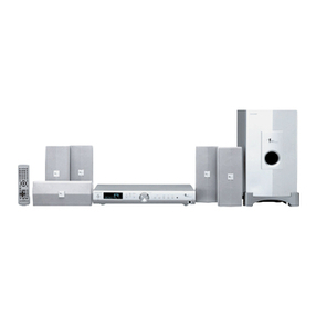
Sharp SD-AT50H User manual

SD-AT50H
No. ?????????????
CONTENTS Page
SAFETY PRECAUTION FOR SERVICE MANUAL ........................................................................................................... 2
IMPORTANT SERVICE NOTES (FOR U.K. ONLY) .......................................................................................................... 2
SPECIFICATIONS ............................................................................................................................................................. 3
NAMES OF PARTS ........................................................................................................................................................... 4
DISASSEMBLY.................................................................................................................................................................. 6
ADDITIONAL DESCRIPTION ............................................................................................................................................ 8
ADJUSTMENT ................................................................................................................................................................... 9
DESCRIPTION OF CIRCUIT FOR 1-BIT UNIT ................................................................................................................. 9
TO CHECK AND CANCEL PROTECT CIRCUIT DETECTION LINE.............................................................................. 10
BLOCK DIAGRAM ........................................................................................................................................................... 11
SCHEMATIC DIAGRAM / WIRING SIDE OF P.W.BOARD............................................................................................. 20
VOLTAGE ........................................................................................................................................................................ 41
NOTES ON SCHEMATIC DIAGRAM .............................................................................................................................. 42
TYPES OF TRANSISTOR AND LED............................................................................................................................... 42
WAVEFORMS OF 1-BIT CIRCUIT .................................................................................................................................. 43
FUNCTION TABLE OF IC................................................................................................................................................ 44
REPLACEMENT PARTS LIST/EXPLODED VIEW
PACKING METHOD (FOR U.K. ONLY)
SERVICE MANUAL
This document has been published to be used
for after sales service only.
The contents are subject to change without notice.
SHARP CORPORATION
• In the interests of user-safety the set should be restored to its
original condition and only parts identical to those specified be
used.
1-BIT DIGITAL HOME CINEMA
MODEL SD-AT50H

SD-AT50H
– 2 –
Precaution to be taken when replacing and servicing the
Laser Pickup.
The AEL (Accessible Emission Level) of Laser Power Output
for this model is specified to be lower than Class 1
Requirements. However, the following precautions must be
observedduringservicingtoprotectyoureyesagainstexposure
to the Laser beam.
(1) When the cabinet has been removed, the power is turned
on without a compact disc, and the Pickup is on a position
outerthanthelead-inposition,theLaserwilllightforseveral
seconds to detect a disc. Do not look into the Pickup Lens.
(2) The Laser Power Output of the Pickup inside the unit and
replacementservicepartshavealreadybeenadjustedprior
to shipping.
(3) No adjustment to the Laser Power should be attempted
when replacing or servicing the Pickup.
(4) Under no circumstances look directly into the Pickup Lens
at any time.
(5)CAUTION-Useofcontrolsoradjustments,orperformance
of procedures other than those specified herein may result
in hazardous radiation exposure.
IMPORTANT SERVICE NOTES (FOR U.K. ONLY)
Beforereturning the unitto the customer after completion of a
repairoradjustmentitisnecessary for thefollowingwithstand
voltage test to be applied to ensure the unit is safe for the
customer to use.
Setting of Withstanding Voltage Tester and set.
Set name set value
Withstanding Voltage Tester
Test voltage 4,240 VPEAK
3,000 VRMS
Set time 6 secs
Set current (Cutoff current) 4 mA
Unit
Judgment
OK: The “GOOD” lamp lights.
NG: The “NG” lamp lights and the buzzer sounds.
PROBE
AC OUT UNIT
SHORT-CIRCUIT
AC POWER
SUPPLY CORD
CONNECT THE PROBE
TO GND OF CHASSIS
SCREW
WITHSTANDING
VOLTAGE TESTER
SAFETY PRECAUTION FOR SERVICE MANUAL
Laser Diode Properties
Material: AIGaAs/InGaAIP
Wavelength: 780 nm/650 nm
Emission Duration: continuous
Laser Output: max. 0.69 mW
ADVERSEL-SYNLIG OG USYNLIG LASERSTRÅLING VED ÅBNING. SE IKKE IND I
STRÅLEN-HELLER IKKE MED OPTISKE INSTRUMENTER.
VARO! AVATTAESSA OLET ALTTIINA NÄKYVÄLLE JA NÄKYMÄTTÖMÄLLE
LASERSÄTEILYLLE ÄLÄ TUIJOTA SÄTEESEEN ÄLÄKÄ KATSO SITÄ OPTISEN
LAITTEEN LÄPI.
VARNING-SYNLIG OCH OSYNLIG LASERSTRÅLNING NÄR DENNA DEL ÄR
ÖPPNAD. STIRRA EJ IN I STRÅLEN OCH BETRAKTA EJ STRÅLEN GENOM
OPTISKT INSTRUMENT.
VAROITUS! LAITTEEN KÄYTTÄMINEN MUULLA KUIN TÄSSÄ
KÄYTTÖOHJEESSA MAINITULLA TAVALLA SAATTAA ALTISTAA
KÄYTTÄJÄN TURVALLISUUSLUOKAN 1 YLITTÄVÄLLE NÄKYVÄLLE JA
NÄKYMÄTTÖMÄLLE LASERSÄTEILYLLE.
VARNING - OM APPARATEN ANVÄNDS PÅ ANNAT SÄTT ÄN I DENNA
BRUKSANVISNING SPECIFICERAS. KAN ANVÄNDAREN UTSÄTTAS FÖR
SYNLIG OCH OSYNLIG LASERSTRÅLNING, SOM ÖVERSKRIDER GRÄNSEN
FÖR LASERKLASS 1.

– 3 –
SD-AT50H
SPECIFICATIONS
FOR A COMPLETE DESCRIPTION OF THE OPERATION OF THIS UNIT, PLEASE REFER
TO THE OPERATION MANUAL.
AV control unit
Dimensions Width: 215 mm (8-1/2")
Height: 58 mm (2-5/16")
Depth: 261 mm (10-5/16")
Weight 1.3 kg (2.9 lbs.)
Audio input terminals Optical digital input (AUX): Square type 1
Coaxial digital input (DVD/CD): RCA type 1
Analog input (DVD/CD): RCA type 1 pair (L/R)
Analog input (TV): RCA type 1 pair (L/R)
Analog input (VCR): RCA type 1 pair (L/R)
Analog input (AUX): RCA type 1 pair (L/R)
Audio output terminal Headphones: 16 - 50 ohms (recommended: 32 ohms)
Other terminals System control 3
Frequency range FM: 87.5 - 108 MHz
AM: 522 - 1,620 kHz
Subwoofer/amplifier unit
Front/centre/surround speakers
Power source AC 230 V, 50 Hz
Power consumption 80 W
Dimensions Width: 260 mm (10-1/4")
Height: 373 mm (14-11/16")
Depth: 421 mm (16-5/8")
Weight 10.3 kg (22.7 lbs.)
Output power Front speakers:
RMS: 100 W (50 W + 50 W) (10 % T.H.D., 1 kHz)
Centre speaker:
RMS: 50 W (10 % T.H.D., 1 kHz)
Surround speakers:
RMS: 100 W (50 W + 50 W) (10 % T.H.D., 1 kHz)
Subwoofer:
RMS: 50 W (10 % T.H.D., 100 Hz)
Amplification system
2.8224 MHz (64fs) 1-bit switching (remarks: fs = 44.1 kHz)
A/D noise shaping 7th-order (delta - sigma) modulation
Terminals Front speakers, Centre speaker, Surround speakers: 4
ohms
System control 2
Subwoofer Type 16 cm (6-1/2") woofer
Maximum input power 100 W
Rated input power 50 W
Impedance 4 ohms
Type Full range speaker system (magnetic shield)
8 cm (3-1/8") Speaker
Maximum input power 100 W
Rated input power 50 W
Impedance 4 ohms
Dimensions Width: 95 mm (3-3/4")
Height: 114 mm (4-1/2")
Depth: 104 mm (4-1/8")
Weight 0.7 kg (1.5 lbs.)/each

SD-AT50H
– 4 –
NAMES OF PARTS
AV control unit
1. RDS Indicator
2. Radio Text Indicator
3. Traffic Programme Indicator
4. Traffic Announcement Indicator
5. Dynamic PTY Indicator
6. Audio Signal Indicators/Speaker Indicators
7. Timer Play Indicator
8. Sleep Indicator
9. FM stereo mode indicator
10. FM Stereo Receiving Indicator
11. On/Stand-by Button
12. Timer Set Indicator
13. Function Button
14. Digital/Analog Input Select or Tuner Band Select Button
15. Volume Up and Down Buttons
16. Remote Sensor
17. Power Indicator
18. Sound Mode Indicators
19. Headphone Socket
20. System Connection Socket (to DVD player)
21. Audio Digital Input Socket
22. Coaxial Digital Audio Input Socket
23. Audio Input Sockets
24. System Connection Sockets (to subwoofer/amplifier unit)
25. AM Loop Aerial Terminal
26. Aerial Earth Terminal
27. FM 75 Ohms Aerial Socket
Display
Front
Back
12 13 14 15
16 18 19
1
7
8
9
32 4 5 6
(1)
(7) (8)
(2) (3) (4) (5) (6)
(9) (
10
)(
11
)(
12
)(
13
)
20 21 22 23 25 26 27
24
17
11
10
MODEL NO. SD-AT50H
(AV CONTROL UNIT)
1-BIT DIGITAL HOME CINEMA
SHARP CORPORATION
MADE IN MALAYSIA
<The bottom of the unit>
(1) Left Front Speaker Indicator (8) Subwoofer Indicator
(2) Front Left Signal Indicator (9) Left Surround Speaker Indicator
(3) Centre Speaker Indicator (10) Surround Left Signal Indicator
(4) Centre Signal Indicator (11) Surround Monaural Signal
Indicator
(5) Front Right Signal Indicator
(6) Right Front Speaker Indicator
(7) Low Frequency Effect Indicator
(12) Surround Right Signal Indicator
(13) Right Surround Speaker Indicator
Subwoofer/amplifier unit
1. Subwoofer
2. Bass Reflex Duct
3. System Connection Socket (to AV control unit)
4. Speaker Terminals
5. System Connection Socket (to AV control unit)
6. AC Power Input Socket
7. Lead Holder
Satellite speaker 5
Front speaker 2: magnetically shielded
Centre speaker 1: magnetically shielded
Surround speaker 2: magnetically shielded
1. Speaker
2. Speaker Terminals
3. Mounting Holes for Stand or Bracket (Optionally available)
Using antislip speaker cushions:
You can install satellite speakers either vertically or horizontally.
Affix the cushions (supplied) to the bottom of the speakers to prevent them from slid-
ing or falling due to vibration.
A sheet of speaker cushions (20 pcs.) is supplied with this product. Use 4 cushions
per speaker.
3
4
5
6
7
21
123
Front Back Bottom
Side
(Vertical position) (Horizontal position)

– 5 –
SD-AT50H
13
12
1
2
3
4
5
6
8
7
9
10
14
15
16
17
18
19
20
22
21
23
24
25
27
28
29
30
31
32
33
34
35
36
37
38
39
26
11
R
emote contro
l
1. Remote Control Transmitter
2. Display Brightness Select or Clock Display Button
3. TV Display Select Button
4. Direct Button
5. Direct Number Buttons
6. Disc Repeat Button
7. Disc A - B Repeat Button
8. DVD Menu Button
9. Cursor Button
10. Disc Fast Reverse, Tuner Preset Down Button
11. Disc Stop Button
12. DVD Chapter Skip, CD/MP3 Disc Track Down or
Tuning Down Button
13. DVD Top Menu Button
14. Digital/Analog Input Select or Tuner Band Select Button
15. Timer Button
16. Sound Mode Select Buttons
17. Dynamic Sound Select Button
18. TV Input Select Button
19. Volume Up and Down Buttons
20. On/Stand-by Button
21. RDS Display Mode Select or DVD Audio Language Select or
CD Audio Output Select Button
22. RDS Programme Type/Traffic Information Search or
DVD Angle Button
23. RDS ASPM (Auto Station Programme Memory) or
DVD Subtitle Button
24. Clear Button
25. DVD Initial Setting Button
26. Amplifier Initial Setting Button
27. CD/MP3 Disc Play Mode Select Button
28. Return Button
29. Enter Button
30. Disc Fast Forward, Tuner Preset Up Button
31. DVD Chapter Skip, CD/MP3 Disc Track Up or Tuning Up Button
32. Disc Play Button
33. Function Button
34. DVD Frame Advance, Disc Pause Button
35. TV On/Stand-by Button
36. DVD Zoom Button
37. Black Level Select Button
38. TV Volume Up and Down Buttons
39. TV Channel Select Buttons
Buttons with "" mark in the illustration can be operated on the
remote control only.

SD-AT50H
– 6 –
1 Top Cabinet 1. Screw ...................... (A1) x5 6-1
2 Bottom Cabinet 1. Leg Cushion............ (B1) x4 6-1
2. Screw ...................... (B2) x4
3. Screw ...................... (B3) x3
3 Rear Panel/ 1. Screw ...................... (C1) x9 6-2
Tuner Unit 2. Flat Cable ............... (C2) x1
4 DSP PWB 1. Screw ...................... (D1) x2 6-2
2.
Top Support Bracket ......
(D2) x1
3. Screw ...................... (D3) x2 6-3
4. PWB Holder ............ (D4) x1
5. Flat Cable ............... (D5) x3
5 Main PWB 1. Screw ...................... (E1) x4 6-3
6 Front Panel 1. Screw .......................(F1) x4 6-3
2. Hook.........................(F2) x2
7 Display PWB 1. Screw ...................... (G1) x6 6-4
DISASSEMBLY
Caution on Disassembly
Follow the below-mentioned notes when disassembling
the unit and reassembling it, to keep it safe and ensure
excellent performance:
1. Be sure to remove the power supply plug from the wall
outlet before starting to disassemble the unit.
2.Take offnylon bands or wire holderswhere they need to
beremovedwhendisassemblingtheunit.Afterservicing
theunit, be sure to rearrangethe leads wherethey were
before disassembling.
3. Take sufficient care on static electricity of integrated
circuits and other circuits when servicing.
Figure 6-3
STEP REMOVAL PROCEDURE FIGURE
Figure 6-2
AV Control Unit
Figure 6-4
Figure 6-1
(A1)x5
ø
3x8mm
Front Panel
Bottom Cabinet
Top Cabinet
(B3)x3
ø
3x8mm
(B2)x4
ø
2x6mm
(B1)x4
(D1)x2
ø
3x8mm
(C1)x2
ø
3x8mm
(C1)x7
ø
3x8mm
Front Panel
Bottom Cabinet
Rear Panel
Tuner Unit
(D2)x1
(C2)x1
DSP PWB
(F1)x2
ø
3x8mm
(D3)x2
ø
3x10mm
(F1)x2
ø
3x8mm
(E1)x2
ø
3x10mm
(F2)x1
(D5)x2 (D5)x1
(F2)x1
(D4)x1
Main PWB
DSP PWB
Front
Panel
Lug Wire
Push
(E1)x2
ø
3x10mm
(G1)x6
ø3x10mm
Display PWB
Front Panel

– 7 –
SD-AT50H
Figure 7-1
Figure 7-2
Figure 7-3
Figure 7-4
Figure 7-5
1 Rear Cover 1. Screw .................... (A1) x16 7-1
2 Subwoofer Stand 1. Screw ...................... (B1) x8 7-1
3 Amp. Unit 1. Screw ...................... (C1) x5 7-2
2. Socket ..................... (C2) x2
4 Power PWB 1. Screw ...................... (D1) x4 7-2
2. Socket ..................... (D2) x5 7-3
5 Limit PWB 1. Screw ...................... (E1) x2 7-3
6 1-Bit Amp. Unit 1. Screw .......................(F1) x8 7-3
7 1-Bit Amp. Cover 1. Screw .................... (G1) x15 7-4
8 1-Bit Amp. PWB 1. Screw ...................... (H1) x6 7-5
9 Subwoofer 1. Screw ....................... (J1) x4 8-1
STEP REMOVAL PROCEDURE FIGURE
Subwoofer/Amplifier Unit
(A1)x4
ø3x16mm
(A1)x1
ø3x12mm
(A1)x2
ø3x8mm
(A1)x2
ø3x8mm (A1)x5
ø3x12mm
(A1)x2
ø3x16mm
(B1)x4
ø4x16mm
(B1)x4
ø4x16mm
Rear Cover
Front Panel
Subwoofer
Stand
(C2)x2
(D1)x4
ø
3x8mm
(C1)x5
ø
3x20mm
Power PWB
Subwoofer
Box
(F1)x2
ø
3x8mm
(E1)x1
ø
3x10mm
(E1)x1
ø
3x8mm
(D2)x1
(D2)x1
(D2)x2
(D2)x1
(F1)x1
ø
3x8mm
(F1)x2
ø
3x8mm
(F1)x1
ø
3x10mm
(F1)x1
ø
3x8mm
(F1)x1
ø
3x8mm
Power PWB
Limit PWB
1-Bit Amp. Unit
(G1)x3
ø3x12mm (G1)x3
ø3x12mm
(G1)x1
ø3x12mm
(G1)x3
ø3x12mm
(G1)x2
ø3x12mm
(G1)x1
ø3x12mm
(G1)x1
ø3x12mm
(G1)x1
ø3x8mm
1-Bit Amp. Cover
Washer
Washer
(H1)x3
ø
3x8mm
1-Bit Amp. PWB
(H1)x3
ø
3x8mm
Be careful of the
silicon grease.

SD-AT50H
– 8 –
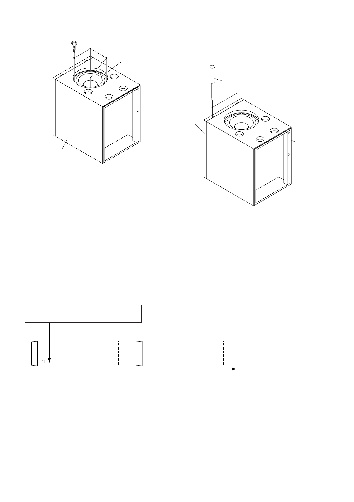
Figure 8-1
Figure 8-2
Subwoofer
(J1)x4
ø4x16mm
Subwoofer
Box
Screwdriver
Front
Panel
Subwoofer
Box
(Note 1)
Wrap a slotted screwdriver with a waste cloth, etc. and insert
it into the gap to remove the front panel. Take great care not
to damage the subwoofer box.
ADDITIONAL DESCRIPTION
Disassembling the top cabinet and bottom cabinet
Remove the 5 screws on the backside of the top cabinet. Raise the rear end by approx. 10 mm, the hooks of the front panel and
then move it backward by approx. 5 mm. Pushing the top of the front panel to separate from keep the top cabinet horizontal and
raise it right above to remove.
Remove the 4 cushions and the 4 screws. On the bottom cabinet push down around the center of the bottom cabinet with a steel
measure or like to remove the tab. Slide the bottom cabinet right backward to remove.
Insertasteelmeasureandpushdownthebottom
cabinet to detach the hook.
The top cabinet is removed

– 9 –
SD-AT50H
Figure 9-4
ADJUSTMENT
Figure 9-3 OUTPUT OFFSET LEVEL
1-bit amplifier's output offset voltage adjustment
Adjust VRA100, VRA101, VRA200, VRA201, VRA300 and
VRA301 so that the DC voltage between speaker terminals +
and - is set to 0 ±5 mV at AC 230 V.
Electronic
Voltage
SO801
AC 230 V
Set
Output:
SpeakerTerminal
+
-
VR : 0
Input : AUX
5
3
1
6
4
2
R-CH Output Offset Adjusument
L-CH Output Offset Adjusument
VRA300 VRA200 VRA100
VRA301
VRA201
VRA101
DESCRIPTION OF CIRCUIT FOR 1-BIT UNIT
(SEE THE WIRING DIAGRAMS ON PAGES 38 AND 39.)
Input section
SignalsfromCNA100 arecoupledbyCA100,CA101,CA200,
CA300 and CA301, and then sent into the A/D converter IC
(ICA100, ICA200, ICA300).
modulation 1-bit converter
Signals from the A/D converter IC (ICA100, ICA200, ICA300)
are converted to 1-bit signals and sent differentially. Refer to
thetechnicalmanualofSM-SX100forthedetailsofconversion
to 1-bit signals.
Dead time and level shift
As for the waveform of 1-bit signals sent through the A/D
converterIC(ICA100,ICA200,ICA300),itsrisetimeisdelayed
by 20 nsec ~ 25 nsec compared to the fall time due to RA114
~ RA117, RA214 ~ RA217, RA314 ~ RA317 and CA106 ~
CA109, CA206 ~ CA209, CA306 ~ CA309 and DA104 ~
DA107, and DA304 ~ DA307. This is for reducing loss of the
switchingcircuitdescribedlater.The1-bitsignalsaresentinto
thebufferIC(theANDgateIC)(ICA101,ICA201,ICA301)and
sent as the shaped waveform.
Low pass filter circuit
1-bit signals switched by the output IC (ICA102, ICA107,
ICA302and ICA307) are converted toanalog signals through
the lowpass filter consisting of LA104 ~ LA107, LA204 ~
LA207, LA304 ~ LA307 and CA114 ~ CA117, CA214 ~
CA217, and CA314 ~ CA317. The low pass filter functions
when a frequency exceeds 20 kHz, and reduces it by approx.
3 dB when it reaches approx. 40 kHz.
Dynamic feedback circuit
The 1-bit signals switched by the output IC (ICA102, ICA107,
ICA302 andICA307) oscillatebetween positiveand negative
voltage. After resistance-division, the signals are fed back to
the A/D converter IC (ICA100, ICA200, ICA300) through NF
resistance 75 kohms (RA130 ~ RA133, RA230 ~ RA233,
RA330 ~ RA333). The peak-to-peak voltage reaches approx.
5 V.

SD-AT50H
– 10 –
TO CHECK AND CANCEL PROTECT CIRCUIT DETECTION LINE
1: In this model the microcomputer (IC301 or IC701) detects
thefollowingmalfunctionsoncepowerissupplied,andcuts
off power from all the parts except for the circuit driving the
microcomputer.
1
Abnormal drop in the output voltage of each regulator
(below approx. 1.5 V)
Power is cut off instantly without display.
2
Output offset over voltage of the 1-bit amplifier
(above approx. DC 2 V)
Power is cut off after “ER_AP02” is displayed.
3
Mains overvoltage of the 1-bit amplifier
(above approx. DC 5.5 A)
Power is cut off instantly without display.
4
Defects in the cooling fan or its drive circuit
(when stopped)
Power is cut off after “FAN LOCK” is displayed.
2: Criteria for abnormality, and checking and cancelling the
detection line
The criteria:
1
The voltage of pin 91 on IC301 (PROTECT) or pin 19
(PROTECT) on IC701.
2
Thevoltageofpin29 (OFFSET)onIC701:Low(below
approx. 1 V) (abnormal) and High (above approx. 2.5
V) (normal) .
3
The voltage of pin 19 (PROTECT) on IC701.
4
Themotorrotationiscontrolledwhenthevoltageofpin
20 (FAN CHK) on IC701 is below approx. 1 V.
The motor stops when it is above approx. 1 V.
If the voltage of pin 21 (FAN LOCK) on IC701 is not
between approx. 0.21 V and 0.9 V whilst the motor
rotation is controlled, it is judged as abnormal.
Checking and cancelling the detection line:
Caution: If the PROTECT/OFFSET detection line is
disconnected in case of
1
,
2
or
3
above, a
protective operation does not function. The
disconnection by output short-circuit of each
regulator may cause the parts or PCBs to burn
outandthereforedonotdisconnectthedetection
line when the cause is not identified.
(Power supply can be detected with an
oscilloscopeor like duringapprox. 0.5 seconds
after an abnormality is found. Note that the
detection would be difficult with a tester as the
voltage rises and falls rapidly.)
11
11
1
Abnormal drop in the output voltage of each regulator
Connect a measuring device (such as an oscilloscope) to
the stabilizing output of the regulator, and turn on the unit.
If the detected voltage is extremely lower than the voltage
on the circuit diagram (below approx. 1.5 V), the regulator
itself or the circuit is defective.
22
22
2
Output offset overvoltage of the 1-bit amplifier
Adjust the voltage of the output offset. If a protective
operation is still activated, QA100 ~ QA103, QA200 ~
QA203 or QA300 ~ QA303 on the 1-bit amplifier could be
defective (the detection circuit of the speaker output DC
voltage).
33
33
3
Mains overvoltage of the 1-bit amplifier
Theunitfunctionsproperlyifpowerissuppliedafterremoving
BIA111 (1-bit amplifier main power supply connector). (No
sound is heard from the speaker.)
* Adjust the output offset voltage after repair.
Ifaprotectiveoperationisstillactivatedevenafterremoving
BIA111,QA413,QA414,QA415,QA410,QA411orQA412
couldbedefective(thedetectionofpowersupplyvoltage).
44
44
4
Defects in the cooling fan or its drive circuit
Connect a measuring device (such as an oscilloscope) to
pin 21 (FANLOCK) on IC701 terminal, and turn on the unit.
Connect the collector of Q822 to GND and make sure the
fan motor rotates properly. If not, check if the motor or fan
isobstructedandthemotoritselfisdefective.Ifalltheabove
arefineand thevoltageofpin21isbelowapprox.0.2Vwith
the collector of Q822 connected to GND, check Q830, its
peripheral circuits or the connection of the fan motor. The
fanmotorcouldbedefectiveifthevoltageofpin21exceeds
approx. 0.91 V right after connecting the collector of Q822
to GND and remains above approx. 0.91 V.

– 11 –
SD-AT50H
Figure 11 BLOCK DIAGRAM (1/9)
ANALOG SIGNAL
INPUT
OUTPUT OFFSET
ADJUSTMENT
+5V
ADIC INSIDE
(IX2815AF)
IN
NF+
A+5V
D+5V
D+5V
OUT+
OUT-NF–
B, S
B, S
B, S
B, S
H-IN
L-IN
H-IN
L-IN
VKK
D+5V
VCC VDD(D+5V)
+POWER
-POWER
+POWER
-POWER
ICA102, ICA107
ICA202, ICA207
ICA302, ICA307
SLA5505M
SWITCHING AUDIO
POWER AMP.
LOW PASS FILTER
LOAD
OFFSET
DETECTION CIRCUIT
NF
+B
A+5V
KIA78M05 KIA78M05
KIA78M05 IN
IN OUT
GND
ICA101, ICA201, ICA301
TC74AC8T
QUAD 2 INPUT AND GATE
OUT
-B
-B +B
-B
GND
GND
+B
D+5V
IN
OUT
GND
REFERENCE
VOLTAGE + 6.5 V
-POWER
DEADTIME CONTROL
(6 CH AVAILABLE)
+
–+
–
+
–
ICA100, ICA200, ICA300
IX2815AF
7TH ORDER ∆∑
MODULATION
CONVERSION LSI
ICA401
KIA7805AP
VOLTAGE
REGULATOR
ICA402
KIA7805AP
VOLTAGE
REGULATOR
ICA400
KIA7806AP
VOLTAGE
REGULATOR
OVERCURRENT/
OVERHEAT DETECTION CIRCUIT

SD-AT50H
– 12 –
Figure 12 BLOCK DIAGRAM (2/9)
LE
D
LED6
LED5
LED4
LED3
LED2LED1
RMS1
GP1UD271
REMOCON SENSOR 21
LED10
SO1
HEADPHONES
LED9
12345678910 11 12
3
Q8 Q1 Q2
Q3
Q4 Q5
Q6
LCD1
V5OUT
V2OUT
VLCD
VLOUT
C1-
C1+
VCC
GND
SDA
SCL
CS
RESET
RXIN
LE
D
LED DRIVER
LED DRIVER
LED
DRIVER
LED DRIVER
LED DRIVER
LED
DRIVER
LED
DRIVER
Q9
LED DRIVER

– 13 –
SD-AT50H
Figure 13 BLOCK DIAGRAM (3/9)
LED7
LED6
D5
LED8
ES
CN502A
BACK_LIGHT
STRLED
KEY_1
LCDSDA
LCDSCL
LCDCS
LCDRESET
DTSLED
STDLED
POWERKEY
DDLED
DPLLED
VIRLED
TIMERLED
LED9V
Q5
Q6
Q7
+5V(D)
+3.7V(UN-SWD)
GND(U-COM)
H.P SW
L-CH
GND(A)
R-CH
RXIN
+5V(D)
+3.3V(SWD)
GND(D)
N
R-CH
L-CH
H.P SW
25
24
23
22
21
20
19
18
17
15
13
12
11
10
9
8
7
6
5
4
3
2
1
16
14
SW2~SW5
LED DRIVER
LED DRIVER
D DRIVER
SW1
TO DSP SECTION

SD-AT50H
– 14 –
Figure 14 BLOCK DIAGRAM (4/9)
CN501A
JT502
VTR/AUX
TERMINAL
Q528
CN503A
Q502
Q501
JT501
DVD/CD/TV
TERMINAL
IC501
BD3811K1
VOLUME IC
80
79
78
77
76
75
74
73
72
71
70
69
68
67
66
65
40
39
38
37
36
35
34
33
32
31
30
29
28
27
26
25
17 16 15 14
1234
5
6
7
8
9
10
11
1213
24 23 18
19
20
21
22
41 42 43 44 45 46 47 48 49 50 51 52 64
6362
61
60
59
58
57
56
55
5453
+5V(D)
RIN
LIN
ROUT3
LOUT3
LOUT2
ROUT2
CCB_CE
CCB_DI
AMP_CLK
LOUT1
ROUT1
AMP_SOUT
TUNER_SM
CCB_DO
CCB_CL
FM_STB
AMP_STB
AMP_INT
AMP_SIN
OUTSW
OUTC
OUTSR
_
OUTSR
_
VOL_CL
VOL_DA
S_MUTE
+12V
CONFIG AGND
HP_R
HP_L
S_MUTE
PROTECT
CONFIG
VOL_CL
VOL_DA
BS_RCH
BS_LCH
TV_LCH
TV_RCH
DVDA_LCH
DVDA_RCH
TUN_L
TUN_R
VTR_RCH
VTR_LCH
AUX
VTR
TV
DVD
R-CH
L-CH
LCH
R-CH
R-CH
L-CH
L-CH
R-CH
R-CH
GND(A)
L-CH
GND(U-COM)
+3.7V(UN-SWD)
GND(A)
+9V(A)
GND(D)
+5V(D)
GOUTC
AGND2
VINSW
GOUTSW
AGND1
IN DSPSL
INDSPC
IN DSPSW
OUTSL
OUTSR
VINSL
VINC
OUTSW
OUTC
VINSR IN2DSP
OUT1(+)
IN DVDSR
VCC
DA
GOUTSR IN1MIX
OUT2(-)
CL
MUTE OUT2(+)
INDVD SW
AGND5
AGND6
VEE
AGND4
DGND OUT1(-)
IN1DSP
INDVDC
IN DVDSL
IN82
AGND8 IN81
IN72
IN71
IN62
OUT2
BBNF1
OUT1
BNF22
BBNF2 IN61
IN52
IN51
BNF12
BNF21
BNF11 IN41
IN42
TNF1 IN32
IN21
GOUT1
AGND9
IN12
IN11
VIN2
GOUT2
ROUT32
ROUT31
AGND10
ROUT11
ROUT22
ROUT21
ROUT12
GOUTSL
AGND3
AGND7
TNF2
VIN1
IN22
IN DSPSR
IN2MIX
IN31
25
24
23
22
8
7
14
11
12
15
6
10
3
1
5
4
2
13
9
19
16
17
21
18
20
1 2 4
3 5 6 8
7 9
TO DSP SECTION
TO DSP SECTION

– 15 –
SD-AT50H
Figure 15 BLOCK DIAGRAM (5/9)
BI507
IC507
BA05ST
SWITCH
REGULATOR
4 2
CNP505
CNP506
IC513
KIA7809AP
VOLTAGE
REGULATOR
3 1
CNP504
Q516
Q518
Q517
IC505
NJM4565D
OPE AMP.
Q514
Q525
Q527
Q526
0
9
8
7
6
5
4
3
2
1
0
9
8
7
6
5
Q504
Q503
1234
5 6 7 8
2
5 3 1
OUTSW
OUTC
OUTSR_RCH
OUTSR_LCH CCB_DO
CCB_CL
CCB_DI
CCB_CE
TUN_R
TUN_L
FMVSM
+5V(D)
OUTC
AGND
OUTSW
AGND
+12V
+12V
+12V
-12V
BS_RCH
BS_LCH
TUN_L
TUN_R
+5V(D)
A_+7V
PROTECT
A_+7V
A_-7V
-12V
TUNER_SM
FM_STB
AMP_SOUT
AMP_STB
AMP_CLK
AMP_SIN
AMP_INT
OUTSR_LCH
OUTSR_RCH
OUTF_RCH
OUTF_LCH
A_-7V
A_-7V
HP_R
HP_L
S_MUTE
GND_D
REG_ON
A.GND
GND
AUX
VTR
R-CH
L-CH
L-CH
R-CH
GND_UCON
GND_A
+
-
+3.7V_(UCON)
D+7.5V
AMP_SIN
AMP_SOUT
GND_D
A+15V
AMP_INT
AMP_STB
AMP_CLK
A-15V
CENTER
SURROUND LCH
SURROUND RCH
FRONT RCH
FRONT LCH
GND
GND
TO POWER
SECTION
SUB WOOFER
VDD
-
+
VSS
+3.7V(UN-SWD)
IN22
-12V(A)
-15V(A)
+7.5V(SWD)
+15V(A)
+12V(A)
CE
DO
FM VSM
GND
L OUT
FM DET
VCC +9V
DI
CL
R OUT
3
1
2
2
4
7
5
1
9
3
11
6
8
01
8
6
11
3
1
9
5
7
2
4
2
1
3
1
01
6
8
1
5
3
7
2
4
TO DSP
SECTION
TO POWER
SECTION
TO TUNER
UNIT
VDDA
MPXIN
VSSA
XOUT
SYR
CE
T1
T2
DI
CL
DO
VDDD
XIN
VSSD
24 23 22 21 20 15 1314
2 3 4
12
8
7
XT01
4.332 MHz
QT01
ICT01
LC72720Y
RDS DECORDER

SD-AT50H
– 16 –
Figure 16 BLOCK DIAGRAM (6/9)
D706 LED805
LED803
LED804
LED806
LED802
LED807
LED809 LED808
CNP901
RL
9
BI901
D
9
21
32
31
30
29
28
27
26
25 16
15
14
13
12
11
10
9
XL701
2 MHz
BI802
BI801
CNP801
RL801
RL802
SO801
SPEAKER
TERMINAL
D801
RL803
CNP803
IC813
KIA4558F
PRE AMP.
8
4
IC811
KIA4558F
PRE AMP.
8
4
IC812
KIA4558F
PRE AMP.
8
4
BI803
D710
24 23 22 21 20 19 18 17
1 2 3456783
123
5 6 7
3 2 1
5 6 7
3 2 1
5 6 7
PROTECT
A_-15V
RLY_+12V
P
AC_DETECT
AMP_INT AMP_INT
T
A
+3.7V(UCON)
+15V
A__+15V
DRIVER
-15V
AMP_CLK
AMP_STB
AMP_SOUT
AMP_INT
AMP_SIN
D_+7.5V
-
B
+15V
SYS_STOP
AC_DETECT
S_S_MUTE
F_S_MUTE
FAN_LOCK
PROTECT
FAN
C_S_MUTE
RESET
+3.7V(UCON)
+3.3V(USWD)
+B_CHECK
OFFSET
SYS_STOP
W_S_MUTE
AMP_STB
TIMING_CK
-B_CONT
POWER
AMP_SIN
AMP_CLK
AC_DETECT
A/D_RESET
BASS-SW
SP_RLY
AMP_SOUT
A_+12V
A_-12V
SP__RLY
SP_RLY SP_RLY
SP__RLY
FAN FAN_LOCK
BASS-SW
PROTECT
OFFSET
A/D_RESET
W_S_MUTE
C_S_MUTE
S_S_MUTE
F_S_MUTE
PROTECT
A_+12V
BASS SW
DRIVER
RESET
IC702
PST9127
RESET
RELAY
DRIVER RELAY
DRIVE
R
VOLTAGE
REGULATOR MOTOR
DRIVER
SWITHING
BUFFER
BUFFER
BUFFER
BUFFER
MUTE
DRIVER
MUTE
DRIVER
MUTE
DRIVER
MUTE
DRIVER
MUTE
DRIVER
M1
FAN MOTOR
Q701
SUBWOOFER
SUBWOOFER
Q705
Q704
Q703 FRONT R-CH
FRONT L-CH
Q829
Q828
Q859
Q818
VDD
-
+ VSS
+
-
Q815
Q816
Q817
Q820
Q814
Q813
+ VDD
- VSS
+
-
Q819
Q812
Q811
Q827
Q830
M
Q822
Q801
-
-
+
+ VSS
VDD
POINT
RESET
L-CH +
L-CH -
R-CH -
R-CH +
R-CH -
L-CH -
L-CH +
FRONT
SURROND
CENTER +
+
-
-
CENTER
L-CH
R-CH
L-CH
R-CH
GND
FRONT
SURROND
R-CH -
L-CH -
L-CH +
SURROND FRONT
L-CH -
R-CH -
L-CH +
R-CH +
CENTER
+
-
GND
R-CH
L-CH
L-CH
CENTER
R-CH
GND
GND
R-CH +
SUB WOOFER
R-CH +
SURROND FRONT
CENTER
SUB WOOFER
Q919
13
11
12
8
1
2
3
4
5
9
7
2
6
5
4
10
3
1
4
3
2
1
1
3
4
5
2
6
8
9
7
4
2
3
1
5
2
6
3
4
8
7
5
1
2
1
3
4
10
9
11
12
6
8
7
5
1
2
3
4
5
6
7
8
9
10
11
12
13
IC701
IX0564AW
SYSTEM
MICROCOMPUTER
+
–
SP6
SUBWOOFER
TO 1-BIT AMP.
SECTION
TO 1-BIT AMP.
SECTION
TO MAIN SECTION
TO 1-BIT AMP.
SECTION
TO 1-BIT AMP.
SECTION
TO MAIN SECTION

– 17 –
SD-AT50H
Figure 17 BLOCK DIAGRAM (7/9)
IC901
STRF6267
SWITCHING
REGULATOR
5
4
2
1
CNP901
RL911
BI901
D920
F901
T3.15A L 250V
D911
3
2 1
PC901
TRS901
IC911
SE-B2
ERROR
AMP.
2
IC912
KIA7812AP
VOLTAGE
REGULATOR
3 1
L901
AC LINE
FILTER
L902
AC LINE
FILTER
D901
D913
3 2
1
IC913
S812C37A
3.7V REGULATOR
3 2
T901
SWITCHING POWER TRANSFORMER
3
3
1
2
1
A_-15V
+
12V
POWER
E
TECT
NT
TIMING_CK TIMING_CK
AC_DETECT AC_DETECT
+3.7V(UCON)
+15V
A__+15V
R
IVER
-15V
AMP_CLK
AMP_STB
AMP_SOUT
AMP_INT
AMP_SIN
D_+7.5V
-B_CONT
C
ON)
V
V
A_+15V
A_-15V
BUFFER
RELAY
DRIVER
Q919 Q925
Q911
Q924
Q922
Q921 Q920
Q918
Q923
Q901 FB/SYNC
Drain
OCP
SYNC
GND
Vin
13
11
12
8
1
2
3
4
5
9
7
2
6
5
4
10
3
1
4
3
2
1
SO901
AC SOCKET
AC 230V, 50 Hz
AC POWER
SUPPLY CORD

SD-AT50H
– 18 –
Figure 18 BLOCK DIAGRAM (8/9)
2
1
3
2
1
CNP507
3 1
3 1
3 1
CN501B
8
7
6
5
4
3
2
1
44
43
42
41
40
39
38
37
36
35
34
33 32 31 30 29 28 27 26 25 24 23
22
21
20
19
18
17
16
15
14
13
12
11
10
9
8
7
6
5
43
2
1
4
1
1
3
1
2
1
1
1
0
9
8
7
6
5
4
3
2
1
8
7
6
5
4
3
2
1
44
43
42
41
40
39 38 37 36 35 34 33 32 31 30 29
28
27
26
25
24
23
22
21
20
19
18
17
16
15
14
13
12
11
10
9
8
7
6
5
4
3
2
1
2
2
2
SDATA1
SCLK
LRCK
SCLK
SDATA1
/EXTMEM
_DSP_INTREQ
_DSP_CS
_DSP_SCDOUT
/EMWR
/EMOE
_DSP_SCDIN
EMAD0
EMAD1
EMAD3
EMAD2
EMAD4
EMAD5
EMAD6
EMAD7
_DSP_SCCLK
EX_CLK
_DSP_SCCLK
_DSP_INTREQ
DSP_SCCLK
DSP_ABOOT
DSP_INTREQ
MCLK
LRCK
AUDATA0
SDATA1
SCLK
AUDATA1
AUDATA2
SCL
SDA
OVF
DVD_ON
DVD_POWER
KEY_OUT
EX_CLK
AUDATA2
DSP_RESET
LRCK
SCLK
MCLK
AUDATA1
AUDATA0
PROTECT
CCB_CL
CCB_DI
AMP_CLK
AMP_SOUT
CCB_CE
CCB_DO
TUNER_SM
AMP_INT
FM_STB
AMP_SN
AMP_STB
_DSP_SCDOUT
_DSP_CS
_DSP_SCDIN
DSP_SCDIN
DSP_SCDOUT
DSP_CS
LRCK
+2.5V(D)
+2.5V(D) +2.5V(D)
IC101
CS493264
DSP
+5V(A)
+5V(D)
+5V(D)
+5V(A)
+5V(A)
+5V(A)
+5V(A)
+3.3V(D)
+3.3V(D)
IC104
74HC07AF
BUFFER AMP.
IC103
TC7WU04U
DUAL2-INPUT
AND GATE
+3.3V(D)
IC112
SI3033LUS
3.3 V REGULATOR
IC111
IX0446AW
VOLTAGE
REGULATOR
IC110
SI3050LUS
VOLTAGE
REGULATOR
<
IC102
AK4586VQ
ADC/DAC/DIR
CONVERTER
IC109
TC7WU04U
DUAL2-INPUT
AND GATE
SO102
SYSTEM CONTROL
TERMINAL
SO101
DVD/CD DIGITAL
INPUT TERMINAL
+5V(D)
GND(U-COM)
+9V(A)
+5V(D)
+2.5V(A)
+5V(D)
+3.7V(UN-SWD)
+3.3V(D)
+2.5V(D)
GND(D)
+5V(A)
GND(A)
LOUT1
LOUT2
LOUT3
ROUT3
ROUT2
ROUT1
RIN
LIN
VCC
GND
3Y 3A
2Y
2A 1Y
1A
RX101
GP1FM521
AUX DIGITAL
INPUT TERMINAL
XL101
12.288 MHz
1A 1Y
2A 2Y
3A
3Y
GND
VCC
PVDD
R
PVSS
RX4
SLAVE
RX3
TST
RX2
I2C
RX1
CAD0/CSN
SCL/CCLK
SDA/CDTI
CAD1/CDTO
INT1
INT0
MCKO
TX
XTI/EXTCLK
XTO
SCLKN2
LRCLKN2
SDATAN2
SCCLK
SCDIN
SCDOUT
CS
INTREQ
EXTMEM
SDATAN1
SCLKN1
LRCLKN1
D0
D1
D2
D3
D4
D5
D6
D7
RD
WR
XMT958
MCLK
SCLK
LRCLK
AUDATA0
AUDATA1
AUDATA2
CLKIN
CLKSEL
FILT2
FILT1
RESET
DD
DC
AGND
VA
DGND3
DGND2
DGND1 VD3
VD2
VD1
DZF2/OVF
VCOM
VREFH
AVDD
AVSS
DZF1
LIN
RIN
ROUT1
ROUT2
ROUT3
LOUT3
LOUT2
LOUT1
PDN
DVSS
DVDD
TVDD
SDTO
SDTI3
SDTI2
SDTI1
LRCK
BICK
3
211
2
3
4
5
6
7
8
9
10
11
12
13
14
15
16
17
18
19
20
21
22
23
24
25
VCC
GND
TO MAIN SECTION

– 19 –
SD-AT50H
Figure 19 BLOCK DIAGRAM (9/9)
CNP507 TP300 CN503B
5 4
3 2
1
100
99
98
97
96
95
94
93
92
91
90
89
88
87
86
85
84
83
82
81
80
79
78
77
76
75
74
73
72
71
70
69
68
67
66
65
64
63
62
61
60
59
58
57
56
55
54
53
52
51
50
49
48
47
46
45
44
43
42
41
40
39
38
37
36
35
34
33
32
31
30 29 28 27 26 25 24 23 22 21 20 19 18 17 16 15 14 13 12 11 10
987654321
TUNER_SM
H.P_SW
DSP_INTREQ
RESET
SYS_STOP
RX_IN
AMP_INT
DSP_RESET
DSP_SCCLK
DSP_CS
DSP_SCDOUT
DSP_SCDIN
FLASH_BUSY
FLASH_SCLK
FLASH_RXD
FLASH_TXD
DTS_LED
STD_LED
DD_LED
TIMER_LED
DSP_UC17
DSP_UC16
DSP_UC15
DSP_ABOOT
ROM
DPL_LED
VIR_LED
VOL_CL
VOL_DA
B_LIGHT
STR_LED
SUB_SP_ON
DIG_FUNC+B
BASS_SW
_S_MUTE
S_MUTE
PROTECT
POWER_KEY
CCB_CL
FM_STB
CCB_CE
CCB_DI
CCB_DO
DVD_POWER
KEY1
LCD_SDA
LCD_SCL
LCD_CS
FLASH_VCC
LCD_RESET
AMP_STB
AMP_CLK
AMP_SN
AMP_SOUT
OVF
KEY_OUT
DVD_ON
SDA
SCL B_LIGHT
RX_IN
POWER_KEY
LCD_SDA
TIMER_LED
LCD_SCL
DTS_LED
LCD_CS
DD_LED
LCD_RESET
DPL_LED
VIR_LED
STD_LED
H.P_SW
STR_LED
KEY1
FLASH_TXD
FLASH_SCLK
FLASH_BUSY
FLASH_RXD
RESET
FLASH_VCC
S_MUTE
SUB_SP_ON
VOL_DA
PROTECT
BASS_SW
VOL_CL
Q401
Q402
Q303
IC302
PST9127N
RESET
IC301
IX0563AW
DSP SYSTEM
MICROCOMPUTER
2
L
US
U
LATOR
IC111
IX0446AW
VOLTAGE
REGULATOR
+3.3V(SWD)
+3.3V(BACK-UP)
+3.3V(UN-SWD)
+9V(A)
+3.3V(UN-SWD)
+3.3V(BACK-UP)
GND(H/P)
L-CH(H/P)
GND(H/P)
L-CH(H/P)
R-CH(H/P)
R-CH(H/P)
+3.3V(BACK-UP)
+3.3V(UN-SWD)
+3.7V(UN-SWD)
RESET
POINT
P47
P50
P51
P52
P53
P54
P55
P56
P57
P60
P61
P62
P63
P64
P65
P66
P70
P71
P72
P73
P74
P75
P76
P77
P80
P81
P82
BYTE
P97
AVCC
VREF
AN0
AVSS
AN1
AN2
AN3
AN4
AN5
AN6
AN7
P00
P01
P02
P03
P04
P05
P06
P07
P10
P11
P12
P13
P14
P15
P16
P17
P20
P21
P22
P23
P24
P25
P26
P43
P27
VSS
P30
VCC
P31
P32
P33
P34
P35
P36
P37
P40
P41
P42
P44
P45
P46
P67
P83
P85
VCC
XIN
VSS
P84
XOUT
RESET
P86
P87
CNVSS
P90
P91
P92
P93
P94
P95
P96
XL301
8.38MHz
3
21
25
24
23
22
21
20
19
18
17
16
15
14
13
12
11
10
9
8
7
6
5
4
3
2
11 3459
8
79 8 7 6 5 4 3 2 1
26
+3.3V(SWD)
+5V(D)
TO MAIN SECTIONTO DISPLAY SECTION

SD-AT50H
– 20 –
A
B
C
D
E
F
G
H
123456
Figure 20 WIRING SIDE OF P.W.BOARD (1/10)
R594
R593
R588
C638
R584
R585
R586
R583
C637
C641 R587 R713A
C578
C587
R615
R600 R601
R602 R603
C582
C588
C642
R648
R505
IC501
R504
C508
C507
R500
R501
R621
C630
C629
C606
C697
C648
R633
C647
R634
RT07
CT14
RT06
RT10
CT13
CT10
CT03
CT04
CT15
R635
R637
C653
R638
C654
R636
R639
C657
R641
C658
R642
R645
C661
C662
R646
C537
R521
R507
R509
C535
C533
R519 R517 R513
R515
R511
R512
R514
R520
R522
C534 C538
R508
R516
R510
R518
C536
R644
C632 C691 C692
R643
R640
C649
R632
R631
C589
RT11
CT11
CT08 CT07
CT02
RT08
RT09
CT06
CN503A
Q517
Q518
R597
R598
R596
R591
R647
R590
R592
Q516
R595
R714A
C634
C640
IC505
C665
C633
C639
C583
C585
R626
R627
ZD502
Q514
D514
Q525
R614
R613
ZD503
C584 Q526
R690
C586
D509
D517
R605
C601
Q527
D516
C598
R606
R604
D518
Q504
R619
D508
R616
R620
R599
C666
Q503
C502
C501
D501
Q501
R649
Q502
D502
Q528
C524 C523
C522
C521
C520
C519
C518
C517
C698
C506
D537
C503
C504
D538
C505
C664
C663
COR501
D507
COR502
R652
BI507 C605
C604 CT09
DT01
CT01
CT05
RT17
C595
C696
C594
R689
IC507
IC513
R611
R612
C596
D526
D525
D527
D528
R651
R688
LT22
LT21
ZD504
CNP504
R608
R607
C645
C646
C651
C652
C655
C656
C659
C660
C531
C529
C527
C525
CN501A
C526
C528
C530
C532
D521
D522
JT501
DVD/CD/TV
TERMINAL
JT502
VTR/AUX
TERMINAL
D523
D524
D520
D519
CNP506
SYSTEM
CONTROL
TERMINAL
C590
CT12
RT01
RT02
RT03
RT04
CNP505
SYSTEM
CONTROL
TERMINAL
C592
C591
D511 D510
FFC501
FFC503
CNS507
RT05
ICT01
XT01
QT01
C701
CN501B
P25 10 - B
TO DSP PWB
25 1
R-CH L-CH
DVD/CD R-CH L-CH
TV R-CH
VTRL-CH R-CH L-CH
AUX
1234 15
789
10
11 12
13
6
234
5678
123
CNP507
P25 10 - G
TO DSP PWB
12
34
78
56
9
10
11
2
14
36
58
7
10
9
12
11 14
13 16
15 18
17 20
19 22
21 24
23
25
3
2
1
3
2
1
41
45
50
55
60
64
65
70
75
80
1510 1520
24 25
30 35 40
1
2
3
4
8
7
6
5
E C B
S
G
D
S
G
D
E
C
B
E
C
B
E
C
B
2468
13579
1
2
3
E
C
B
B
C
E
B C E
MAIN PWB-A1
1
3
1
1
2
3
3
5
2
4
CN503B
P24 1 - F
TO DSP PWB
19
WH
GY
GY
WH
GY
GY
1
24
20
15 10
5
13 12
E C B
Other manuals for SD-AT50H
2
Table of contents
Other Sharp Home Theater System manuals

Sharp
Sharp HT-X1H User manual

Sharp
Sharp SD-AT100H User manual

Sharp
Sharp HT-DV50H User manual

Sharp
Sharp SD-AS10W User manual

Sharp
Sharp HT-DV40U User manual

Sharp
Sharp HT-X1H User manual

Sharp
Sharp HT-CN300W User manual

Sharp
Sharp HT-SB100 User manual

Sharp
Sharp HT-M750H User manual

Sharp
Sharp HT-SL72 User manual

Sharp
Sharp HT-CN400DVW User manual

Sharp
Sharp SD-AT1000 User manual

Sharp
Sharp HT-CN410DVH User manual

Sharp
Sharp HT-SB60 User manual

Sharp
Sharp HT-SBW460 User manual

Sharp
Sharp HT-C21DS1 User manual

Sharp
Sharp HT-DP2500W User manual

Sharp
Sharp HT-SB603 User manual

Sharp
Sharp HT-SB60 User manual

Sharp
Sharp HT-SB95 User manual