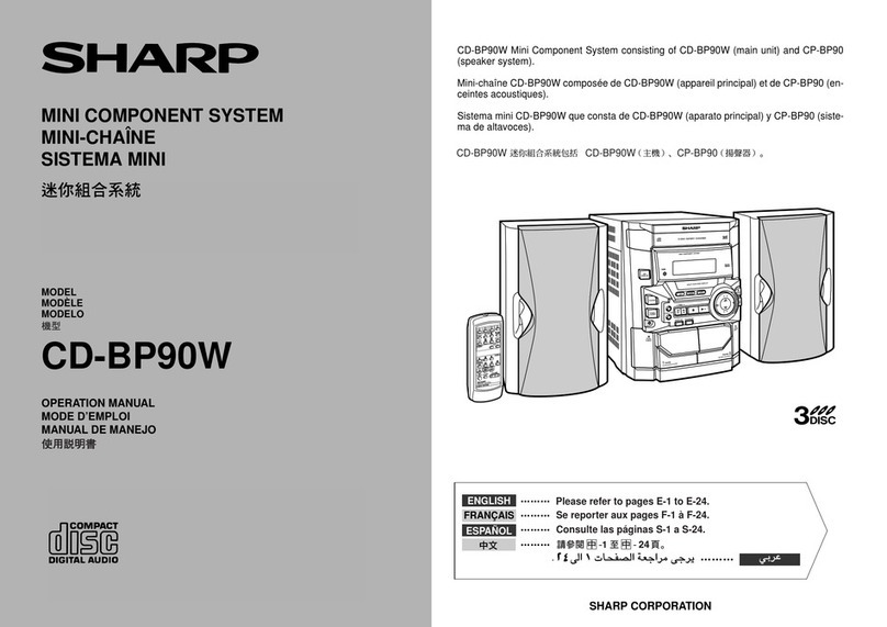
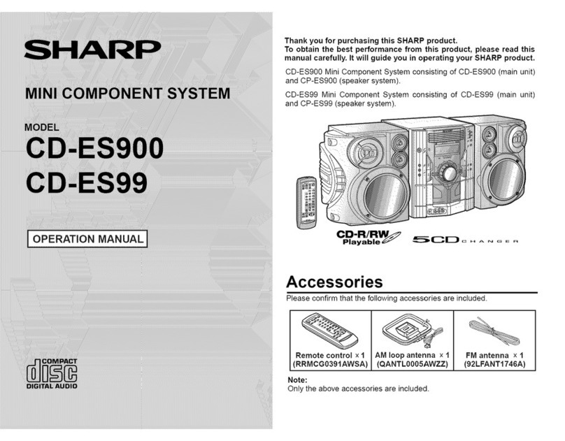
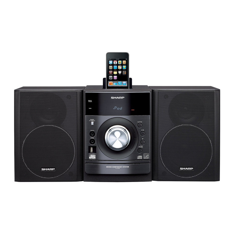
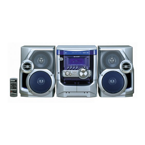
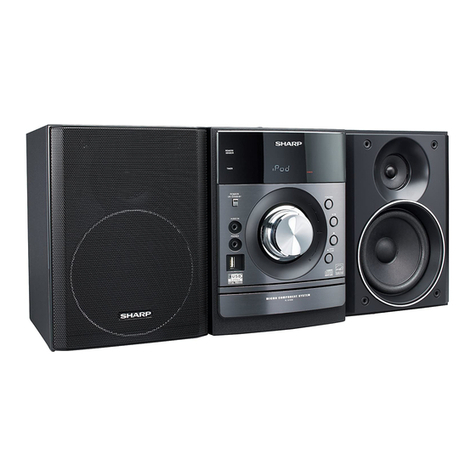
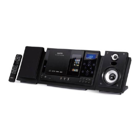
Sharp DK-AP2 User manual

DK-AP2/DK-AP2(BK)
– 1
MUSIC SYSTEM FOR iPod
SERVICE MANUAL
No. S7737DKAP2H//
This document has been published to be used for
after sales service only.
The contents are subject to change without notice.
DK-AP2
(
BK
)
MODEL
• In the interests of user-safety the set should be restored to
its original condition and only parts identical to those
specified be used.
iPod is a trademark of Apple Inc.,
registered in the U.S and other countries
.
PRECAUTIONS FOR USING LEAD-FREE SOLDER
CHAPTER 1. GENERAL DESCRIPTION
[1] Important Service Notes (for U.K. only) ..........1-1
[2] Specifications .................................................1-1
[3] Name Of Parts................................................1-2
CHAPTER 2. MECHANICAL DESCRIPTION
[1] Disassembly .................................................. 2-1
CHAPTER 3. DIAGRAMS
[1] Block Diagram................................................3-1
CHAPTER 4. CIRCUIT DESCRIPTION
[1] Voltage .......................................................... 4-1
CHAPTER 5. CIRCUIT SCHEMATICS AND PARTS
LAYOUT
[1] Notes On Schematic Diagram.......................5-1
[2] Types Of Transistor And LED........................5-1
[3] Chart Of Connecting Wires............................5-2
[4] Schematic Diagram.......................................5-4
[5] Wiring Side Of PWB......................................5-14
CHAPTER 6. OTHERS
[1] Function Table Of IC......................................6-1
PARTS GUIDE
Parts marked with " " are important for maintaining the safety of the set. Be sure to replace these parts with
specified ones for maintaining the safety and performance of the set.
CONTENTS
DK-AP2
MODEL
MUSIC SYSTEM FOR iPod
SHARP CORPORATION
(For Europe, U.K.)
(For Europe, U.K.)
•Note for users in U.K.
Recording and playback of any material may require
consent which SHARP is unable to give. Please refer
particularly to the provisions of Copyright Act 1956, the
Performers Protection Acts 1963 and 1972 and subsequent
statutory enactments and orders.

DK-AP2/DK-AP2(BK)
– 2
PRECAUTIONS FOR USING LEAD-FREE SOLDER
1.Employing lead-free solder
Example:
Indicates lead-free solder of tin, silver and copper.
Lead-free wire solder for servicing
Ref No. Description
Parts No.
PWB-A 92LPWB6822MANS
92LPWB6758LEDSPWB-C
MAIN (A1), iPOD (A2)
PWB-B 92LPWB6822SWHS
POWER SWITCH (B1), PLAY SWITCH (B2), BATTERY POSITIVE (B3),
BATTERY NEGATIVE (B4)
LED
"MAIN, iPOD, POWER SWITCH, PLAY SWITCH, BATTERY POSITIVE, BATTERY NEGATIVE, LED PWB" of this
model employs lead-free solder.The LF symbol indicates lead-free solder, and is attached on the PWB and
service manuals.The alphabetical character following LF shows the type of lead-free solder.
2.
Using lead-free wire solder
When fixing the PWB soldered with the lead-free solder, apply lead-free wire solder. Repairing with conventional
lead wire solder may cause damage or accident due to cracks.
As the melting point of lead-free solder (Sn-Ag-Cu) is higher than the lead wire solder by 40°C, we recommend
you to use a dedicated soldering bit, if you are not familiar with how to obtain lead-free wire solder or soldering
bit, contact our service station or service branch in your area.
3.
Soldering
As the melting point of lead-free solder (Sn-Ag-Cu) is about 220°C which is higher than the conventional lead
solder by 40°C,and as it has poor solder wet ability, you may be apt to keep the soldering bit in contact with the
PWB for extended period of time. However, since the land may be peeled of for the maximum heat-resistance
temperature of parts may be exceeded, remove the bit from the PWB as soon as you confirm the steady
soldering condition.
Lead-free solder contains more tin, and the end of the soldering bit may be easily corrected.Make sure to turn
on and off the power of the bit as required.If a different type of solder stays on the tip of the soldering bit, it is
alloyed with lead-free solder. Clean the bit after every use of it.
When the tip of the soldering bit is blackened during use, file it with steel wool or fine sand paper.
Be careful when replacing parts with polarity indication on the PWB silk.
i

DK-AP2/DK-AP2(BK)
1 – 3
CHAPTER 1.
GENERAL DESCRIPTION
[2] Specifications
DK-AP2/DK-AP2(BK)
[1] Important Service Notes (for U.K. only)
Before returning the unit to the customer after completion of a repair or adjustment it is necessary for the following withstand voltage test to be
applied to ensure the unit is safe for the customer to use.
Setting of Withstanding Voltage Tester and set.
Set name set value
Withstanding Voltage Tester
Test voltage 4,240 VPEAK
3,000 VRMS
Set time 6 secs
Set current (Cutoff current) 4 mA
Unit
Judgment
OK: The “GOOD” lamp lights.
NG: The “NG” lamp lights and the buzzer sounds.
PROBE
AC OUT AC/DC
ADAPTOR
SHORT-CIRCUIT
AC POWER
SUPPLY CORD
CONNECT THE PROBE
TO SHELL OF DC CONNECTOR
WITHSTANDING
VOLTAGE TESTER
FOR A COMPLETE DESCRIPTION OF THE OPERATION OF THIS UNIT, PLEASE REFER TO THE OPERATION MANUAL.
General
DK-AP2/DK-AP2(BK) for U.K.
General
CAUTION: “Danger of explosion if battery is incorrectly replaced. Replace only with the same
or equivalent type”.
*This power consumption value is obtained when in the power
*stand-by mode.
Power source DC IN 6V 2A: AC/DC adaptor
(AC 100 - 240 V ~ 50/60 Hz)
DC IN 3V [ “AA” size (UM/SUM-3, R6 or
HP-7) battery x 4]
Power
consumption Power on : 3.8 W
Power stand-by: 0.2 W (*)
Output power Speakers:
RMS: 3.8 W (1.9 W + 1.9 W) (DIN 45 324)
Speaker 1-way type speaker system
Speakers: 5 cm (2") - 6 ohms - Full Range
Speaker maximum
input power 3.8 W/Channel
Speaker rated
input power 1.9 W/Channel
Output terminals Video output: 1Vp-p
Input terminals Auxiliary (audio signal):
500 mV/47 k ohms
Dimensions Width: 380 mm (15")
Height: 157 mm (6-2/5")
Depth: 221 mm (8-7/10")
Weight 1.2 kg (2.65 lbs) * This power consumption value is obtained when in the power
stand-by mode.
Power source DC IN 6V 2A: AC/DC adaptor
(AC 100 - 240V ~ 50/60 Hz)
DC IN 3V [ “AA” size (UM/SUM-3, R6 or
HP-7) battery x 4]
Power
consumption Power on : 3.8 W
Power stand-by: 0.2 W*
Output power Speakers:
RMS: 3.8 W (1.9 W + 1.9 W) (10%T.H.D.)
Speaker 1-way type speaker system
Speakers:5 cm (2") - 6 ohms - Full Range
Speaker maximum
input power 3.8 W/Channel
Speaker rated
input power 1.9 W/Channel
Output terminals Video output: 1Vp-p
Input terminals Auxiliary (audio signal):
500 mV/47 k ohms
Dimensions Width: 380 mm (15")
Height: 157 mm (6-2/5")
Depth: 221 mm (8-7/10")
Weight 1.2 kg (2.65 lbs)
1 – 1

DK-AP2/DK-AP2(BK)
1 – 4
Top view
1. Power Indicator
2. E SOUND Indicator
3. Skip Down Button
4. Play/Pause Button
5. Skip Up Button
6. iPod Dock
7. Volume Down Button
8. ON/STAND-BY Button
9. Volume Up Button
10. Stand-by Indicator
Side view
1. DC Input Socket
2. Auxiliary Input Socket
3. Video Out Socket
Bottom view
1. Battery Compartment
[3] Names Of Parts
DC IN 6V AUX IN
VIDEO
OUT
3
12
12
34 5 6 7 8 9 10
- VOL +
-
ON/STAND-BY
-
M
U
S
I
C
S
Y
S
T
E
M
D
K
-
A
P
2
ESOUND
STAND-BY
12
34 5 6 7 8 9 10
- VOL +
-
ON/STAND-BY
-
M
U
S
I
C
S
Y
S
T
E
M
D
K
-
A
P
2
ESOUND
STAND-BY
1
Remote control
1. Remote ControlTransmitter
2. On/Stand-by Button
3. Volume Up and Down Buttons
4. Skip Down Button
5. Skip Up Button
6. Dimmer Button
7. Display Button
8. Play Mode Button
9. E SOUND Button
10. Play/Pause Button
6
7
8
9
10
3
2
4
5
1
1 – 2

DK-AP2/DK-AP2(BK)
2 – 1
CHAPTER 2. MECHANICAL DESCRIPTION
[1] Disassembly
Caution on disassembly
Follow the below-mentioned notes when disassembling
the unit and reassembling it, to keep it safe and ensure
excellent performance:
1) Be sure to remove the power supply plug from the
wall outlet before starting to disassemble the unit.
2) Take off nylon bands or wire holders where they
need to be removed when disassembling the unit.
After servicing the unit, be sure to rearrange the
leads where they were before disassembling.
3) Take sufficient care on static electricity of integrated
circuits and other circuits when servicing.
1 Bottom Cover 1
2 Battery Positive PWB/
Battery Negative PWB
2
3 Speaker Box Ass’y 3
1. Screw ............................(C1) X 3
2. Socket ...........................(C2) X 2
1. Screw ............................(E1) X 3
1. Screw ............................(K1) X 8
1. Screw ............................(D1) X 1
2. Screw ............................(D2) X 4
3. Screw ............................(D3) X 1
4. Socket ...........................(D4) X 1
5. Flat Cable ......................(D5) X 1
1. Screw ............................ (F1) X 4
1. Screw ..........................(G1) X 10
1. Screw ............................(H1) X 1
2. Screw ............................(H2) X 2
1. Open Battery Cover................A1
2. Screw ............................(A2) X 4
3. Screw ............................(A3) X 1
4. Socket ...........................(A4) X 1
1. Screw ............................(B1) X 2
4 Main PWB 4
5 iPOD PWB 5
6 Play Switch PWB/
Power Switch PWB
5
7 Back Cabinet 6
8 LED PWB 7
9 Speaker 8
STEP REMOVAL PROCEDURE FIGURE
Figure 2
Figure 3
(B1)x2
M2.6x6mm
(A4)x1
Battery
Negative PWB
Bottom Cover
Speaker Box Ass’y
(C2)x2
From
Main PWB
Battery
Positive PWB
From
Main PWB
(C1)x3
M3x10mm
Bottom Cabinet
Figure 1
(A3)x1
M3x8mm
Bottom Cover
Main Unit
(A2)x4
M3x8mm
A1
Battery Cover

DK-AP2/DK-AP2(BK)
2 – 2
Figure 7
Figure 8
(D1)x1
M3x8mm
(D3)x1
M3x8mm
(D2)x4
M3x10mm
Bottom Cabinet
Main PWB
To
Battery PWB
(D5)x1
From Switch PWB
(D4)x1
From iPOD PWB
Main Chassis
Figure 4
Figure 5
Figure 6
Bottom Cabinet
(F1)x2
M2.6x8mm
(E1)x2
M2.6x8mm
(F1)x2
M2.6x8mm
(G1)x10
M3x10mm
Speaker Box Ass’y
Power Switch PWB
Play Switch PWB
iPOD PWB
(H1)x1
M3x10mm
(H2)x2
M3x10mm
LED Holder
Front Panel Ass’y
LED PWB
(K1)x4
M3x8mm
(K1)x4
M3x8mm Speaker
Speaker Wire
Speaker
BLUE
RED
Front Panel Ass’y
Back Cabinet

DK-AP2/DK-AP2(BK)
2 – 3
-MEMO-

DK-AP2/DK-AP2(BK)
3 – 1
CHAPTER 3. DIAGRAMS
[1] Block Diagram
Figure 1: BLOCK DIAGRAM (1/2)

DK-AP2/DK-AP2(BK)
3 – 2
Figure 2: BLOCK DIAGRAM (2/2)

DK-AP2/DK-AP2(BK)
4 – 1

CHAPTER 4.
CIRCUIT DESCRIPTION
[1] Voltage
IC101 IC102 IC103
PIN
NO
VOLTAGE
(V)
PIN
NO
VOLTAGE
(V)
PIN
NO
VOLTAGE
(V)
PIN
NO
VOLTAGE
(V)
1 3.44 1 1.65 1 1.62 9 1.02
2 3.46 2 1.66 2 1.63 10 1.64
3 123.30mV 3 1.65 3 1.64 11 1.62
4 3.46 4 1.90mV 4 2.10mV 12 1.63
5 3.45 5 1.65 5 3.30 13 3.29
6 3.47 6 1.66 6 3.30 14 3.29
7 4.93 7 1.65 7 2.10mV 15 1.64
8 3.43 8 3.30 8 1.03 16 1.64
9 2.11
10 3.47
IC104 IC600
PIN
NO
VOLTAGE
(V)
PIN
NO
VOLTAGE
(V)
PIN
NO
VOLTAGE
(V)
PIN
NO
VOLTAGE
(V)
1 77.10mV 17 200.40mV 1 3.29 17 1.63
2 138.20mV 18 350.20mV 2 3.29 18 -200.80mV
3 4.98 19 46.50mV 3 3.29 19 -166.40mV
4 4.98 20 94.50mV 4 0.20mV 20 185.50mV
5 2.46 21 4.98 5 3.29 21 2.46
6 2.42 22 2.48 6 3.27 22 1.62
7 3.29 23 -80.30mV 7 -8.60mV 23 0.10mV
8 4.98 24 4.96 8 3.29 24 0.00
9 2.48 25 4.98 9 0.20mV 25 3.29
10 0.50mV 26 3.29 10 1.57 26 1.65
11 20.50mV 27 2.42 11 1.53 27 3.04
12 4.98 28 2.46 12 1.40mV 28 0.88
13 0.80mV 29 0.60mV 13 -3.20mV 29 0.50mV
14 7.20mV 30 2.47 14 1.03 30 0.20mV
15 10.50mV 31 -10.70mV 15 -0.30mV 31 0.00
16 12.40mV 32 -24.30mV 16 -0.40mV 32 0.10mV
IC801 IC802 IC803 IC804
PIN
NO
VOLTAGE
(V)
PIN
NO
VOLTAGE
(V)
PIN
NO
VOLTAGE
(V)
PIN
NO
VOLTAGE
(V)
1 3.29 1 3.29 1 3.29 1 1.35
2 -1.40mV 2 -0.10mV 2 -0.80mV 2 527.00mV
3 2.47 3 1.25 3 1.26 3 1.94
4 3.26 4 3.30 4 3.29 4 -1.10mV
5 5.91 5 5.92 5 5.92 5 5.91
61.23
IC805 IC806 IC807 72.22
PIN
NO
VOLTAGE
(V)
PIN
NO
VOLTAGE
(V)
PIN
NO
VOLTAGE
(V)
85.89
1 -1.00mV 1 3.29 1 3.26
2 -1.10mV 2 -0.10mV 2 3.24
3 3.27 3 -0.30mV 3 3.29
4 3.29 4 3.29 4 3.26
5 3.29 5 -0.80mV 5 3.29
6 3.29 6 3.29
7 -0.80mV 7 -1.10mV
8 2.06 8 0.81
9 1.24 9 0.82
10 3.29 10 3.26
11 1.63 11 -1.00mV
12 2.06 12 0.82
13 2.46 13 7.40mV
14 3.29 14 3.29

DK-AP2/DK-AP2(BK)
4 – 2
IC809 IC810
PIN
NO
VOLTAGE
(V)
PIN
NO
VOLTAGE
(V)
PIN
NO
VOLTAGE
(V)
PIN
NO
VOLTAGE
(V)
1 0.60mV 11 0.21 1 2.29 9 2.28
2 -0.30mV 12 1.22 2 2.28 10 3.50mV
3 3.29 13 2.46 3 0.10mV 11 3.50mV
4 3.29 14 3.29 4 0.10mV 12 83.30mV
5 -0.40mV 15 100.20mV 5 0.10mV 13 5.01
6 25.50mV 16 0.82 6 78.50mV 14 5.01
7 3.29 17 0.82 7 3.50mV 15 5.01
8 3.29 18 0.82 8 3.50mV 16 188.80mV
9 3.29 19 0.82
10 -0.20mV 20 3.29
IC811 IC813
PIN
NO
VOLTAGE
(V)
PIN
NO
VOLTAGE
(V)
1 5.92 1 6.21
2 4.98 2 0.00
3 0.20mV 3 5.01
4 4.98
5 2.98

DK-AP2/DK-AP2(BK)
4 – 3
-MEMO-

DK-AP2/DK-AP2(BK)
5 – 1
CHAPTER 5. CIRCUIT SCHEMATICS AND PARTS LAYOUT
[1] Notes On Schematic Diagram
•Resistor:
To differentiate the units of resistors, such symbol as
K and M are used: the symbol K means 1000 ohm
and the symbol M means 1000 kohm and the resis-
tor without any symbol is ohm-type resistor.
Besides, the one with “Fusible” is a fuse type.
• Capacitor:
To indicate the unit of capacitor, a symbol P is used:
this symbol P means pico-farad and the unit of the
capacitor without such a symbol is microfarad. As to
electrolytic capacitor, the expression “capacitance/
withstand voltage” is used.
(CH), (TH), (RH), (UJ): Temperature compensation
(ML): Mylar type
(P.P.): Polypropylene type
• Schematic diagram and Wiring Side of P.W.Board
for this model are subject to change for
improvement without prior notice.
• The indicated voltage in each section is the one
measured by Digital Multimeter between such a
section and the chassis with no signal given.
1. In the tuner section,
indicates FM stereo
•Parts marked with “ ” ( ) are
important for maintaining the safety of the set. Be
sure to replace these parts with specified ones for
maintaining the safety and performance of the set.
[2] Types Of Transistor And LED
REF. NO DESCRIPTION POSITION
SW301 POWER ON / STAND-BY ON—OFF
SW302 VOLUME UP ON—OFF
SW303 VOLUME DOWN ON—OFF
SW304 PLAY/PAUSE ON—OFF
SW305 FORWARD ON—OFF
SW306 REVERSE ON—OFF
KRC107S
KTC3875 GR
KRA102S
KTC2875B
B
(3)
E
(1)
C
(2)
TOP
VIEW
TOP VIEW
KIA78D05
VIEW
FRONT
3 2 1
D1SS119
MA111
IN5820
SK24A
MA21038
RB160M30
Anode
Cathode
A304VT2H
A343BD2S2
A304AD2E
1 - INPUT (Vin)
2 - OUTPUT (VO)
3 - GND
4 - VOSENSE
5 - ON/OFF CTRL (VC)
VIEW
FRONT
12345
KiA278R05

DK-AP2/DK-AP2(BK)
5 – 2
[3] Schematic Diagram
Figure 5-1: MAIN SCHEMATIC DIAGRAM (1/6)
A
B
C
D
E
F
G
H
123456

DK-AP2/DK-AP2(BK)
5 – 3
Figure 5-2: MAIN SCHEMATIC DIAGRAM (2/6)
78 9 10 11 12

DK-AP2/DK-AP2(BK)
5 – 4
Figure 5-3: MAIN SCHEMATIC DIAGRAM (3/6)
13 14 15 16 17 18

DK-AP2/DK-AP2(BK)
5 – 5
Figure 5-4: MAIN SCHEMATIC DIAGRAM (4/6)
A
B
C
D
E
F
G
H
123456

DK-AP2/DK-AP2(BK)
5 – 6
Figure 5-5: MAIN SCHEMATIC DIAGRAM (5/6)
78 9 10 11 12

DK-AP2/DK-AP2(BK)
5 – 7
Figure 5-6: MAIN SCHEMATIC DIAGRAM (6/6)
13 14 15 16 17 18

DK-AP2/DK-AP2(BK)
5 – 8
Figure 5-7: IPOD SCHEMATIC DIAGRAM (1/2)
Other manuals for DK-AP2
4
This manual suits for next models
1
Table of contents
Other Sharp Stereo System manuals

Sharp
Sharp CD-BA3100 User manual

Sharp
Sharp AQUOS CD-BA250 User manual

Sharp
Sharp CD-X9G/H User manual

Sharp
Sharp CD-DD4500 User manual

Sharp
Sharp XL-55W User manual

Sharp
Sharp MD X5 User manual

Sharp
Sharp CD-XP160W User manual

Sharp
Sharp GX-CD5100W User manual

Sharp
Sharp CD-DD4500 User manual

Sharp
Sharp MD-X8 User manual

Sharp
Sharp CD-C662 User manual

Sharp
Sharp XL-T300H User manual

Sharp
Sharp CD-DD4500 User manual

Sharp
Sharp CD-CH1500W User manual

Sharp
Sharp CD-DV999W User manual

Sharp
Sharp XL-HP700H User manual

Sharp
Sharp CD-DP900H User manual

Sharp
Sharp CD-BA3100H User manual

Sharp
Sharp SD-EX100H User manual

Sharp
Sharp SD-CX1W(BL) User manual