Accessories
supplied
AM
loop
antenna
(1)
FM
wire
antenna
(1)
SYSTEM
CONTROL
cord
(1)
(TA-AV531)
Remote
Commander
RM-U521
(1)
(TA-AV531}
RM-U421
(1)
(TA-AV431)
Sony
batteries
SUM-3
(NS)
(2)
Audio
signal
connecting
cord
(phono
plug
x
2
<>
phono
plug
X
2)
(1)
SYSTEM
CONTROL
1
cord
(1)
SYSTEM
CONTROL
2
cord
(1)
SYSTEM
CONTROL
3
cord
(1}
(The
SYSTEM
CONTROL
1
and
3
is
equipped
on
the
TC-W431.)
(TA-AV431)
Design
and
specifications
are
subject
to
change
without
notice.
TABLE
OF
CONTENTS
Section
Title
Page
SECTION
1.
GENERAL
...........ccccccccsssccsecsssssrnsencnmersesseses
3
SE
ARAVA
Se
tect
sadtestoe
tinted
eels
credasten
Racers
eset
uate
soreness
3
PTAA
VSS
lice
sessiiiscvestessieastiios
Gidea
ie
oe
ouedoes
eet
es
as
4
SECTION
2.
IC
PIN
FUNCTIONS
uu...
eeeeeeeeeees
5
SECTION
3.
DIAGRAMS
3-1.
Circuit
Boards
Location
........ccccccccssccscsscssesevsssecevescsasevaeseseevarecers
9
3-2.
Semiconductor
Lead
Layouts
...........c:ccccsesesesesssssssesssscssssssssseevens
9
3-3,
"BlOCK
Diagram
ss
tinecinureiinvivensine
urea
natn
aera
10
3-4.
Printed
Wiring
Board
*
MAIN
Section
eicssscistcosises
dhescestaevadepadieasstesyaassvicnssrvasdiseivacccderss
13
|
3-5.
Schematic
Diagram
@
MAIN
SéCHiON
ceccecsiessecavessecesvois
lis
sssiastectvietsctesbeveitucksstetevateuveane
17
3-6.
Schematic
Diagram
*
DISPLAY
Section...
ciina
ccs
aiieas
wehitieeiniiniagnanhdeencs
21
3-7,
IC
BIOCK
Diagrams
..........ccccecsccssscsesseeescsseserssscssvensacecsscsussenssscaess
23
SECTION
4.
EXPLODED
VIEWS
4-1.
Front
Panel
Section
0.0...
ccccccsssssssesseecssessevssssssssecscsevesseseenessaes
25
4-22.
TBOard:
Section
cdivviesssidcesdacasrassvdsnvestegraacsscatian
svat
sariacusisoeceteiupaseess
26
SECTION
5.
ELECTRICAL
PARTS
LIST
........0..
27
SAFETY
CHECK-OUT
After
correcting
the
original
service
problem,
perform
the
following
safety
checks
before
releasing
the
set
to
the
customer:
Check
the
antenna
terminals,
metal
trim,
‘‘metallized”’
knobs,
screws,
and
all
other
exposed
metal
parts
for
AC
leakage.
Check
leakage
as
described
below.
LEAKAGE
TEST
The
AC
leakage
from
any
exposed
metal
part
to
earth
ground
and
from
all
exposed
metal
parts
to
any
exposed
metal
part
having
a
return
to
chassis,
must
not
exceed
0.5mA
(500
microampers).
Leakage
current
can
be
measured
by
any
one
of
three
methods.
1.
A
commercial
leakage
tester,
such
as
the
Simpson
229
or
RCA
WT-540A.
Follow
the
manufacturers’
instructions
to
use
these
instru-
ments.
2.
A
battery-operated
AC
milliammeter.
The
Data
-
Precision
245
digital
multimeter
is
suitable
for
this
job.
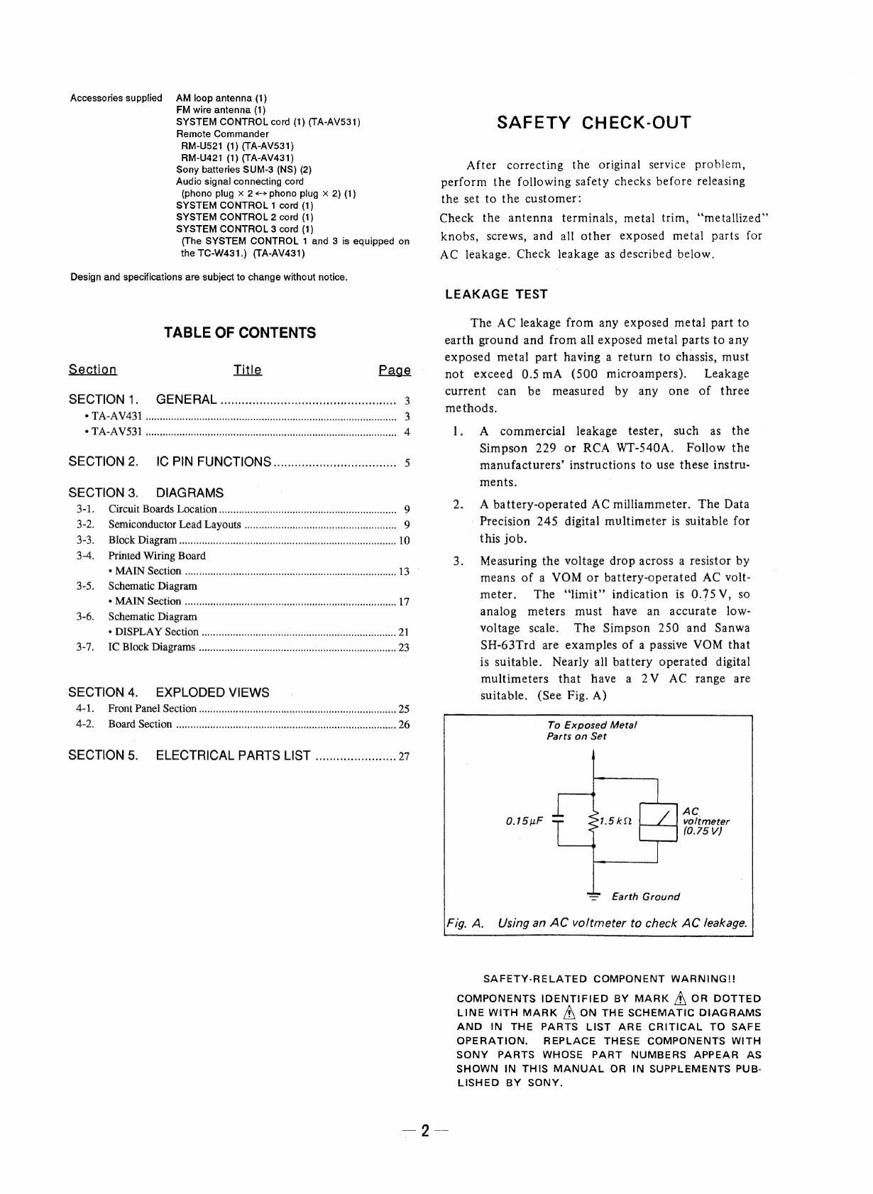
3.
Measuring
the
voltage
drop
across
a
resistor
by
means
of
a
VOM
or
battery-operated
AC
volt-
meter.
The
“limit”
indication
is
0.75
V,
so
analog
meters
must
have
an
accurate
low-
voltage
scale.
The
Simpson
250
and
Sanwa
SH-63Trd
are
examples
of
a
passive
VOM
that
is
suitable.
Nearly
all
battery
operated
digital
multimeters
that
have
a
2V
AC
range
are
suitable.
(See
Fig.
A)
To
Exposed
Metal
Parts
on
Set
AC.
vo/tmeter
P|
(0.78)
=
Earth
Ground
Fig.
A.
Using
an
AC
voltmeter
to
check
AC
leakage.
SAFETY-RELATED
COMPONENT
WARNING!!
COMPONENTS
IDENTIFIED
BY
MARK
A
OR
DOTTED
LINE
WITH
MARK
A
ON
THE
SCHEMATIC
DIAGRAMS
AND
IN
THE
PARTS
LIST
ARE
CRITICAL
TO
SAFE
OPERATION.
REPLACE
THESE
COMPONENTS
WITH
SONY
PARTS
WHOSE
PART
NUMBERS
APPEAR
AS
SHOWN
IN
THIS
MANUAL
OR
IN
SUPPLEMENTS
PUB-
LISHED
BY
SONY.


